US6680237B2 - Method of manufacturing deep trench capacitor - Google Patents
Method of manufacturing deep trench capacitor Download PDFInfo
- Publication number
- US6680237B2 US6680237B2 US09/967,709 US96770901A US6680237B2 US 6680237 B2 US6680237 B2 US 6680237B2 US 96770901 A US96770901 A US 96770901A US 6680237 B2 US6680237 B2 US 6680237B2
- Authority
- US
- United States
- Prior art keywords
- layer
- deep trench
- collar
- forming
- conductive layer
- Prior art date
- Legal status (The legal status is an assumption and is not a legal conclusion. Google has not performed a legal analysis and makes no representation as to the accuracy of the status listed.)
- Expired - Lifetime, expires
Links
Images


Classifications
-
- H—ELECTRICITY
- H10—SEMICONDUCTOR DEVICES; ELECTRIC SOLID-STATE DEVICES NOT OTHERWISE PROVIDED FOR
- H10B—ELECTRONIC MEMORY DEVICES
- H10B12/00—Dynamic random access memory [DRAM] devices
- H10B12/01—Manufacture or treatment
- H10B12/02—Manufacture or treatment for one transistor one-capacitor [1T-1C] memory cells
- H10B12/03—Making the capacitor or connections thereto
- H10B12/038—Making the capacitor or connections thereto the capacitor being in a trench in the substrate
- H10B12/0385—Making a connection between the transistor and the capacitor, e.g. buried strap
Definitions
- the present invention relates to a method of manufacturing the capacitor of a dynamic random access memory (DRAM). More particularly, the present invention relates to a method of manufacturing a deep trench capacitor.
- DRAM dynamic random access memory
- DRAM dynamic random access memory
- DRAM capacitors can be roughly divided into two major types, a stacked capacitor or a deep trench capacitor. Yet, both types of capacitors face similar technical problems in manufacturing as dimension of constituent semiconductor devices in a silicon chip is reduced
- HSG hemispherical grains
- a deep trench capacitor is formed inside a substrate, planarization is not a problem.
- the deep trench structure facilitates the fabrication of small memory devices.
- producing semiconductor devices having a line width of about 0.2 ⁇ m demands the production of a trench having an aspect ratio of up to 35:1.
- To advance to the production of device with a line width of 0.17 ⁇ m or less even less space is available for housing each trench and hence the difficulties in shaping a deep trench by photolithographic and etching processes are deeply intensified.
- gap-filling materials necessary for filling the deep trench must be improved.
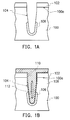
- FIGS. 1A through 1D are schematic cross-sectional views showing the progression of steps for fabricating a conventional deep trench type capacitor.
- a patterned mask layer 102 is formed over a substrate 100 .
- the mask layer 102 and the substrate 100 are sequentially etched to form a deep trench 104 .
- a doped region 106 is formed at the bottom of the deep trench 104 to serve as a storage electrode of the subsequently formed deep trench capacitor.
- a conformal dielectric layer 108 is formed over the exposed surface of the deep trench 104 .
- a chemical vapor deposition is conducted to fill up the deep trench 104 and form a conductive layer 110 .
- the conductive layer 110 can be a doped polysilicon layer, for example. Because the gap-filling capacity of polysilicon deteriorates as critical dimensions of the deep trench 104 are reduced, a seam 112 is formed in the innermost portion of the conductive layer 110 .
- a portion of the conductive layer 110 at the top of the deep trench 104 is removed to form a conductive layer 110 a at the bottom of the deep trench 104 .
- the dielectric layer 108 at the top end of the deep trench 104 is also removed.
- the seam 112 is exposed
- a collar oxide layer 114 conformal to the exposed surface is formed over the substrate 100 so that the upper surface of the mask layer 102 and the interior surface of the deep trench 104 are covered.
- an anisotropic etching is conducted to remove the collar oxide layer 114 above the mask layer 102 and the conductive layer 110 a and expose the conductive layer 110 a. Thereafter, a conductive layer 116 that completely fills the deep trench 104 is formed so that the conductive layer 110 a and the conductive layer 116 are electrically connected. The conductive layer 116 is etched back so that the upper surface of the conductive layer 116 is lower than the upper surface 100 a of the substrate 100 . The exposed collar oxide layer 114 on the sidewalls near the top of the deep trench 104 is removed. Conductive material is deposited into the deep trench 104 to form a conductive layer 118 . The conductive layer 118 and the conductive layer 116 are electrically connected and are also electrically connected to the substrate 100 . The conductive layer 110 a, the conductive layer 116 and the conductive layer 118 together form the upper electrode of the deep trench capacitor
- the presence of the seam 112 in the conductive layer 110 leads to the opening of the seam 112 after the etching back process. Consequently, the collar oxide layer 114 at the bottom of the trench after deposition is thicker than the collar oxide layer 114 above the mask layer 102 . Furthermore, a portion of the oxide filling material may leak into the seam 112 . Hence, when the collar oxide layer 114 is etched, the collar oxide layer 114 over the mask layer 102 may be completely removed before the collar oxide material 114 a above the conductive layer 110 a and within the seam 112 . The residual collar oxide material 114 a between the conductive layer 110 a and the conductive layer 116 forms an electrical barrier that may lead to memory cell failure and low product yield.
- one object of the present invention is to provide a method of manufacturing a deep trench capacitor capable of removing residual collar oxide material from a seam and preventing electrical connectivity problem between a first conductive layer and a second conductive layer within the deep trench. Ultimately, failure of single cells is reduced and product yield of semiconductor devices is improved.
- the invention provides a method of manufacturing a deep trench capacitor.
- a substrate having a patterned mask layer thereon and a deep trench therein is provided.
- a doped region is formed in the substrate around the bottom of the deep trench.
- a conformal capacitor dielectric layer and a first conductive layer are sequentially formed completely filling the deep trench. Due to miniaturization, the deep trench has a high aspect ratio.
- a seam is formed in the first conductive layer within the deep trench after conductive material is deposited into the trench. Thereafter, a portion of the first conductive layer is removed to open up the seam.
- a conformal collar oxide layer and a collar liner are formed over the substrate.
- Material forming the collar liner layer and material forming the collar oxide layer both have a high etching selectivity ratio. A portion of the collar liner layer is removed so that the collar liner layer on the sidewalls of the deep trench is retained. The collar oxide layer above the mask layer and the first conductive layer is removed. Using the collar liner layer on the sidewalls of the deep trench as a mask, the residual collar oxide layer above the first conductive layer and within the seam is removed. The collar liner layer on the sidewalls of the deep trench is subsequently removed. Finally, a second conductive layer and a second conductive layer are sequentially formed filling the deep trench.
- a collar liner layer is formed over the collar oxide layer on the interior sidewalls of the deep trench.
- the collar liner layer having a lower etching rate than the oxide material can serve as a protective layer for removing any residual oxide layer at the upper surface of the first conductive layer.
- the collar oxide layer can have a constant thickness after an etching operation.
- the collar liner layer can protect the collar oxide layer on the sidewalls of the deep trench, over-etching is less damaging. Hence, extended etching for completely removing any residual collar oxide material above the first conductive layer and within the seam is possible. Without any residual collar oxide material serving as an electrical barrier, memory cell failure is reduced and product yield is increased.
- FIGS. 1A through 1D are schematic cross-sectional views showing the progression of steps for fabricating a conventional deep trench type capacitor.
- FIGS. 2A through 2J are schematic cross-sectional views showing the progression of steps for fabricating a deep trench capacitor according to one preferred embodiment of this invention.
- FIGS. 2A through 2J are schematic cross-sectional views showing the progression of steps for fabricating a deep trench capacitor according to one preferred embodiment of this invention.
- a patterned mask layer 202 is formed over a substrate 200 .
- the mask layer can be a silicon nitride layer formed, for example, by chemical vapor deposition (CVD) followed by a photolithographic and etching operation.
- An etching operation such as a dry etching is conducted to form a deep trench 204 inside the substrate 200 .
- a doped insulation layer 206 is formed over the interior sidewalls of the deep trench 204 .
- the doped insulation layer 206 can be an arsenic doped silicon oxide layer formed, for example, by in-situ doping of ions in a chemical vapor deposition (CVD).
- a photoresist layer 208 is formed at the bottom of the deep trench 204 such that the deep trench 204 is only partially filled and the upper surface of the photoresist layer 208 is below the upper surface 200 a of the substrate 200 .
- the doped insulation layer 206 not covered by the photoresist layer 208 is removed.
- the doped insulation layer 206 is removed, for example, by wet etching using a buffer hydrofluoric acid (BHF) or a diluted hydrofluoric acid (DHF) etching agent.
- BHF buffer hydrofluoric acid
- DHF diluted hydrofluoric acid
- a conformal insulation layer (not shown) is formed over the substrate 200 covering the mask layer 202 and the deep trench 204 .
- An anisotropic etching is conducted to remove a portion of the insulation layer, thereby forming spacers 210 on the sidewalls of the deep trench 204 and exposing the upper surface of the photoresist layer 208 .
- the spacers 210 can be a silicon oxide layer formed, for example, by chemical vapor deposition using tetra-ethyl-ortho-silicate (TEOS)/Ozone (O 3 ) as reaction gases.
- TEOS te
- the photoresist layer 208 is removed.
- a thermal treatment of the substrate is carried out so that the dopants inside the doped insulation layer 206 a diffuse into the substrate 200 at the bottom of the deep trench 204 to form a doped region 212 .
- the doped region 212 serves a storage electrode of the subsequently formed deep trench capacitor.
- spacers 210 since sidewalls in the upper section of the deep trench 204 are covered by spacers 210 , dopants in the doped insulation layer 206 a are prevented from migrating too far and hence limiting the doped region 212 around the bottom portion of the deep trench 204 .
- the doped insulation layer 206 a at the bottom of the deep trench 204 and the spacers 210 on the sidewalls in the upper portion of the deep trench 204 are removed, for example, by wet etching using an etching agent such as buffered hydrofluoric (BHF) acid or diluted hydrofluoric (DHF) acid.
- BHF buffered hydrofluoric
- DHF diluted hydrofluoric
- a conformal capacitor dielectric layer 214 is formed over the substrate 200 covering the exposed surface of the deep trench 204 .
- the capacitor dielectric layer 214 can be an oxide/nitride composite layer formed, for example, by thermal oxidation or low-pressure chemical vapor deposition.
- a conductive layer 216 is formed, completely filling the deep trench 204 .
- the conductive layer 216 can be a doped polysilicon layer formed, for example, by in-situ ion doping of ion in a chemical vapor deposition to form a doped polysilicon layer (not shown) over the substrate 200 . Thereafter, excess doped polysilicon material above the deep trench 204 is removed by chemical-mechanical polishing (CMP). Because the deep trench 204 has a rather narrow opening, gap-filling capacity of doped polysilicon material is poor. Ultimately, a seam 218 is formed near the center of the polysilicon conductive layer 216 .
- CMP chemical-mechanical polishing
- the conductive layer 216 in the upper section of the deep trench 204 is removed so that a conductive layer 216 a remains at the bottom section of the deep trench 204 .
- the capacitor dielectric layer 214 in the upper section of the deep trench 204 not covered by the conductive layer 216 a is also removed. Since the upper surface of the conductive layer 216 a is below the upper surface 200 a of the substrate 200 , the seam 218 opens up after a portion of the conductive layer 216 is removed.
- the conductive layer 216 is removed, for example, by dry etching or wet etching.
- a conformal collar oxide layer 220 is formed over the substrate 200 .
- the collar oxide layer 220 covers the upper surface of the mask layer 202 and the exposed surface of the deep trench 204 .
- the collar oxide layer 220 is formed, for example, by chemical vapor deposition.
- a conformal collar liner layer 222 is formed over the substrate 200 covering the collar oxide layer 220 .
- the collar liner layer 222 can be any material having an etching selectivity different from the collar oxide layer 220 , for example, silicon nitride, polysilicon, silicon or silicon oxynitride.
- the collar liner layer 22 is formed, for example, by conducting a plasma-enhanced chemical vapor deposition or a low-pressure chemical vapor deposition.
- the conformal collar liner layer 222 is etched back by conducting an anisotropic etching operation.
- a portion of the collar liner layer 222 is removed so that only a collar liner layer 222 a remains attached to the sidewalls of the deep trench 204 .
- the collar liner layer 222 is etched using the collar oxide layer 220 as an etching stop. Hence, material constituting the collar liner layer 222 must have an etching rate considerably lower than the material constituting the collar oxide layer 220 .
- the collar oxide layer 220 on the upper surface of the mask layer 202 and the upper section of the conductive layer 216 a are removed.
- the collar oxide layer 220 is removed by performing an anisotropic etching operation, for example.
- the seam 218 opens up after the conductive layer 216 is etched.
- the collar oxide layer 220 on the conductive layer 216 a has a thickness greater than the collar oxide layer 220 on the mask layer 202 and a portion of the oxide material may leak into the opened seam 218 .
- the collar oxide layer 220 on top of the mask layer is completely removed while residual collar oxide material 220 a remains above the conductive layer 216 a and within the seam 218 after the collar oxide layer 220 is etched back.
- This layer of residual collar oxide material 220 a forms a barrier layer that prevents the conductive layer from making good electrical contact with a subsequently formed conductive layer 224 .
- the residual collar oxide material 220 a on the conductive layer 216 a and within the seam 218 is removed.
- the residual collar oxide material 220 a is removed by dry etching or wet etching using diluted hydrofluoric (DHF) acid as an etching agent. Since the etching rate of the collar liner layer 222 differs from the collar oxide layer 220 , the collar oxide material 220 a above the conductive layer 216 a and within the seam 218 is easily removed by etching. Thickness of the collar oxide layer 220 in the upper section of the deep trench 204 remains constant after the etching due to the presence of the protective collar liner layer 222 a.
- DHF diluted hydrofluoric
- the collar liner layer 222 a on the sidewalls of the deep trench 204 is removed to expose the collar oxide layer 220 .
- the collar liner layer 222 is a polysilicon layer
- the step of removing the collar liner layer 222 a to expose the collar oxide layer 220 can be skipped.
- a conductive layer 224 that completely fills the deep trench 204 is formed. Because no residual oxide material remains on top of the conductive layer 216 a, the conductive layer 224 is able to form a good electrical contact with the underlying conductive layer 216 a.
- the conductive layer 224 can be a doped polysilicon layer formed, for example, by performing an in-situ ion doping in a chemical vapor deposition to form a doped silicon layer (not shown) and conducting a chemical-mechanical polishing (CMP) to remove any excess doped polysilicon material above the deep trench.
- CMP chemical-mechanical polishing
- the conductive layer 224 is etched so that the upper surface of the conductive layer 224 is below the upper surface 200 a of the substrate 200 .
- the exposed collar oxide layer 220 lining the upper section of the deep trench 204 is next removed.
- Another conductive layer 226 is formed, completely filling the deep trench 204 .
- the conductive layer 226 can be a doped polysilicon layer formed, for example, by performing an in-situ ion doping in a chemical vapor deposition and the conducting a chemical-mechanical polishing (CMP) to remove excess doped polysilicon layer above the deep trench 204 .
- CMP chemical-mechanical polishing
- a collar liner layer is formed over the collar oxide layer on the interior sidewalls of the deep trench. Since the collar liner layer has a lower etching rate than the oxide material, the collar liner layer can serve as a protective layer in the process of removing any residual oxide layer on the upper surface of the first conductive layer. Hence, with the protective collar liner layer, the collar oxide layer can have a constant thickness after etching.
- the collar liner layer can protect the collar oxide layer on the sidewalls of the deep trench, over-etching does not have a serious effect on the device. Therefore, extended etching to remove completely any residual collar oxide material above the first conductive layer and within the seam is possible. Without any residual collar oxide material serving as an electrical barrier, memory cell failure is reduced and product yield is increased.
Landscapes
- Engineering & Computer Science (AREA)
- Manufacturing & Machinery (AREA)
- Semiconductor Memories (AREA)
- Semiconductor Integrated Circuits (AREA)
Abstract
A method of manufacturing a deep trench capacitor. A deep trench is formed in a substrate. A conformal capacitor dielectric layer and a first conductive layer are sequentially formed, completely filling the deep trench. The first conductive layer has a seam. The first conductive layer is etched to open up the seam. A collar oxide layer is formed over the interior surface of the deep trench. A collar liner layer is formed over the collar oxide layer inside the deep trench. Using the collar liner layer as a mask, the collar oxide material above the first conductive layer and within the seam is removed. The collar liner layer is removed. Finally, a second conductive layer and a third conductive layer are sequentially formed inside the deep trench.
Description
1. Field of Invention
The present invention relates to a method of manufacturing the capacitor of a dynamic random access memory (DRAM). More particularly, the present invention relates to a method of manufacturing a deep trench capacitor.
2. Description of Related Art
With advances made in semiconductors regarding deep sub-micron manufacturing technique, dimensions of devices have reduced correspondingly. With size reduction, space for accommodating a capacitor in a dynamic random access memory (DRAM) unit is also reduced. However, the storage capacity of a computer must increase due to a general increase in size of software programs. Such conflicting demands indicate the need for a change in the manufacturing method of DRAM.
DRAM capacitors can be roughly divided into two major types, a stacked capacitor or a deep trench capacitor. Yet, both types of capacitors face similar technical problems in manufacturing as dimension of constituent semiconductor devices in a silicon chip is reduced
Most conventional semiconductor capacitors have a stacked type structure. At present, major methods for increasing effective surface area of a stacked capacitor includes depositing hemispherical grains (HSG) and shaping the capacitor surfaces into crown, fin, cylinder or extended structures. Although the stacked capacitor enjoys much popularity, planarization is still a big fabrication issue demanding much attention especially when size of each memory device is reduced by miniaturization.
Because a deep trench capacitor is formed inside a substrate, planarization is not a problem. In fact, the deep trench structure facilitates the fabrication of small memory devices. However, producing semiconductor devices having a line width of about 0.2 μm demands the production of a trench having an aspect ratio of up to 35:1. To advance to the production of device with a line width of 0.17 μm or less, even less space is available for housing each trench and hence the difficulties in shaping a deep trench by photolithographic and etching processes are deeply intensified. Furthermore, gap-filling materials necessary for filling the deep trench must be improved.
Nevertheless, for 0.17 μm line width generation of deep trench DRAM capacitors, one major factor that determines the failure of a single memory cell is whether the interface between a first conductive layer and a second conductive layer inside the deep trench structure is conductive or not. Hence, how to maintain conduction at the interface between the first and second conductive layer inside the trench is of major importance.
FIGS. 1A through 1D are schematic cross-sectional views showing the progression of steps for fabricating a conventional deep trench type capacitor. As shown in FIG. 1A, a patterned mask layer 102 is formed over a substrate 100. The mask layer 102 and the substrate 100 are sequentially etched to form a deep trench 104. A doped region 106 is formed at the bottom of the deep trench 104 to serve as a storage electrode of the subsequently formed deep trench capacitor.
As shown in FIG. 1B, a conformal dielectric layer 108 is formed over the exposed surface of the deep trench 104. A chemical vapor deposition is conducted to fill up the deep trench 104 and form a conductive layer 110. The conductive layer 110 can be a doped polysilicon layer, for example. Because the gap-filling capacity of polysilicon deteriorates as critical dimensions of the deep trench 104 are reduced, a seam 112 is formed in the innermost portion of the conductive layer 110.
As shown in FIG. 1C, a portion of the conductive layer 110 at the top of the deep trench 104 is removed to form a conductive layer 110 a at the bottom of the deep trench 104. Meanwhile, the dielectric layer 108 at the top end of the deep trench 104 is also removed. When the layer of conductive material near the top is removed, the seam 112 is exposed A collar oxide layer 114 conformal to the exposed surface is formed over the substrate 100 so that the upper surface of the mask layer 102 and the interior surface of the deep trench 104 are covered.
As shown in FIG. 1D, an anisotropic etching is conducted to remove the collar oxide layer 114 above the mask layer 102 and the conductive layer 110 a and expose the conductive layer 110 a. Thereafter, a conductive layer 116 that completely fills the deep trench 104 is formed so that the conductive layer 110 a and the conductive layer 116 are electrically connected. The conductive layer 116 is etched back so that the upper surface of the conductive layer 116 is lower than the upper surface 100 a of the substrate 100. The exposed collar oxide layer 114 on the sidewalls near the top of the deep trench 104 is removed. Conductive material is deposited into the deep trench 104 to form a conductive layer 118. The conductive layer 118 and the conductive layer 116 are electrically connected and are also electrically connected to the substrate 100. The conductive layer 110 a, the conductive layer 116 and the conductive layer 118 together form the upper electrode of the deep trench capacitor
However, in the aforementioned deep trench capacitor manufacturing process, the presence of the seam 112 in the conductive layer 110 leads to the opening of the seam 112 after the etching back process. Consequently, the collar oxide layer 114 at the bottom of the trench after deposition is thicker than the collar oxide layer 114 above the mask layer 102. Furthermore, a portion of the oxide filling material may leak into the seam 112. Hence, when the collar oxide layer 114 is etched, the collar oxide layer 114 over the mask layer 102 may be completely removed before the collar oxide material 114 a above the conductive layer 110 a and within the seam 112. The residual collar oxide material 114 a between the conductive layer 110 a and the conductive layer 116 forms an electrical barrier that may lead to memory cell failure and low product yield.
To remove all residual collar oxide material 114 a above the conductive layer 110 a and within the seam 112, a prolonged etching is required. However, by extending the etching period, thickness of the collar oxide layer lining the sidewalls of the deep trench may be reduced and other device structures may be damaged due to over-etching.
Accordingly, one object of the present invention is to provide a method of manufacturing a deep trench capacitor capable of removing residual collar oxide material from a seam and preventing electrical connectivity problem between a first conductive layer and a second conductive layer within the deep trench. Ultimately, failure of single cells is reduced and product yield of semiconductor devices is improved.
To achieve these and other advantages and in accordance with the purpose of the invention, as embodied and broadly described herein, the invention provides a method of manufacturing a deep trench capacitor. A substrate having a patterned mask layer thereon and a deep trench therein is provided. A doped region is formed in the substrate around the bottom of the deep trench. A conformal capacitor dielectric layer and a first conductive layer are sequentially formed completely filling the deep trench. Due to miniaturization, the deep trench has a high aspect ratio. Hence, a seam is formed in the first conductive layer within the deep trench after conductive material is deposited into the trench. Thereafter, a portion of the first conductive layer is removed to open up the seam. A conformal collar oxide layer and a collar liner are formed over the substrate. Material forming the collar liner layer and material forming the collar oxide layer both have a high etching selectivity ratio. A portion of the collar liner layer is removed so that the collar liner layer on the sidewalls of the deep trench is retained. The collar oxide layer above the mask layer and the first conductive layer is removed. Using the collar liner layer on the sidewalls of the deep trench as a mask, the residual collar oxide layer above the first conductive layer and within the seam is removed. The collar liner layer on the sidewalls of the deep trench is subsequently removed. Finally, a second conductive layer and a second conductive layer are sequentially formed filling the deep trench.
In this invention, a collar liner layer is formed over the collar oxide layer on the interior sidewalls of the deep trench. Hence, the collar liner layer having a lower etching rate than the oxide material can serve as a protective layer for removing any residual oxide layer at the upper surface of the first conductive layer. With the protective collar liner layer, the collar oxide layer can have a constant thickness after an etching operation.
Furthermore, since the collar liner layer can protect the collar oxide layer on the sidewalls of the deep trench, over-etching is less damaging. Hence, extended etching for completely removing any residual collar oxide material above the first conductive layer and within the seam is possible. Without any residual collar oxide material serving as an electrical barrier, memory cell failure is reduced and product yield is increased.
It is to be understood that both the foregoing general description and the following detailed description are exemplary, and are intended to provide further explanation of the invention as claimed.
The accompanying drawings are included to provide a further understanding of the invention, and are incorporated in and constitute a part of this specification. The drawings illustrate embodiments of the invention and, together with the description, serve to explain the principles of the invention. In the drawings,
FIGS. 1A through 1D are schematic cross-sectional views showing the progression of steps for fabricating a conventional deep trench type capacitor; and
FIGS. 2A through 2J are schematic cross-sectional views showing the progression of steps for fabricating a deep trench capacitor according to one preferred embodiment of this invention.
Reference will now be made in detail to the present preferred embodiments of the invention, examples of which are illustrated in the accompanying drawings. Wherever possible, the same reference numbers are used in the drawings and the description to refer to the same or like parts.
FIGS. 2A through 2J are schematic cross-sectional views showing the progression of steps for fabricating a deep trench capacitor according to one preferred embodiment of this invention. As shown in FIG. 2A, a patterned mask layer 202 is formed over a substrate 200. The mask layer can be a silicon nitride layer formed, for example, by chemical vapor deposition (CVD) followed by a photolithographic and etching operation. An etching operation such as a dry etching is conducted to form a deep trench 204 inside the substrate 200.
A doped insulation layer 206 is formed over the interior sidewalls of the deep trench 204. The doped insulation layer 206 can be an arsenic doped silicon oxide layer formed, for example, by in-situ doping of ions in a chemical vapor deposition (CVD). A photoresist layer 208 is formed at the bottom of the deep trench 204 such that the deep trench 204 is only partially filled and the upper surface of the photoresist layer 208 is below the upper surface 200 a of the substrate 200.
As shown in FIG. 2B, the doped insulation layer 206 not covered by the photoresist layer 208 is removed. The doped insulation layer 206 is removed, for example, by wet etching using a buffer hydrofluoric acid (BHF) or a diluted hydrofluoric acid (DHF) etching agent. Thereafter, a conformal insulation layer (not shown) is formed over the substrate 200 covering the mask layer 202 and the deep trench 204. An anisotropic etching is conducted to remove a portion of the insulation layer, thereby forming spacers 210 on the sidewalls of the deep trench 204 and exposing the upper surface of the photoresist layer 208. The spacers 210 can be a silicon oxide layer formed, for example, by chemical vapor deposition using tetra-ethyl-ortho-silicate (TEOS)/Ozone (O3) as reaction gases.
As shown in FIG. 2C, the photoresist layer 208 is removed. A thermal treatment of the substrate is carried out so that the dopants inside the doped insulation layer 206 a diffuse into the substrate 200 at the bottom of the deep trench 204 to form a doped region 212. The doped region 212 serves a storage electrode of the subsequently formed deep trench capacitor. In addition, since sidewalls in the upper section of the deep trench 204 are covered by spacers 210, dopants in the doped insulation layer 206 a are prevented from migrating too far and hence limiting the doped region 212 around the bottom portion of the deep trench 204. The doped insulation layer 206 a at the bottom of the deep trench 204 and the spacers 210 on the sidewalls in the upper portion of the deep trench 204 are removed, for example, by wet etching using an etching agent such as buffered hydrofluoric (BHF) acid or diluted hydrofluoric (DHF) acid.
As shown in FIG. 2D, a conformal capacitor dielectric layer 214 is formed over the substrate 200 covering the exposed surface of the deep trench 204. The capacitor dielectric layer 214 can be an oxide/nitride composite layer formed, for example, by thermal oxidation or low-pressure chemical vapor deposition. A conductive layer 216 is formed, completely filling the deep trench 204. The conductive layer 216 can be a doped polysilicon layer formed, for example, by in-situ ion doping of ion in a chemical vapor deposition to form a doped polysilicon layer (not shown) over the substrate 200. Thereafter, excess doped polysilicon material above the deep trench 204 is removed by chemical-mechanical polishing (CMP). Because the deep trench 204 has a rather narrow opening, gap-filling capacity of doped polysilicon material is poor. Ultimately, a seam 218 is formed near the center of the polysilicon conductive layer 216.
As shown in FIG. 2E, the conductive layer 216 in the upper section of the deep trench 204 is removed so that a conductive layer 216 a remains at the bottom section of the deep trench 204. Meanwhile, the capacitor dielectric layer 214 in the upper section of the deep trench 204 not covered by the conductive layer 216 a is also removed. Since the upper surface of the conductive layer 216 a is below the upper surface 200 a of the substrate 200, the seam 218 opens up after a portion of the conductive layer 216 is removed. The conductive layer 216 is removed, for example, by dry etching or wet etching. A conformal collar oxide layer 220 is formed over the substrate 200. The collar oxide layer 220 covers the upper surface of the mask layer 202 and the exposed surface of the deep trench 204. The collar oxide layer 220 is formed, for example, by chemical vapor deposition.
As shown in FIG. 2F, a conformal collar liner layer 222 is formed over the substrate 200 covering the collar oxide layer 220. The collar liner layer 222 can be any material having an etching selectivity different from the collar oxide layer 220, for example, silicon nitride, polysilicon, silicon or silicon oxynitride. The collar liner layer 22 is formed, for example, by conducting a plasma-enhanced chemical vapor deposition or a low-pressure chemical vapor deposition.
As shown in FIG. 2G, the conformal collar liner layer 222 is etched back by conducting an anisotropic etching operation. A portion of the collar liner layer 222 is removed so that only a collar liner layer 222 a remains attached to the sidewalls of the deep trench 204. The collar liner layer 222 is etched using the collar oxide layer 220 as an etching stop. Hence, material constituting the collar liner layer 222 must have an etching rate considerably lower than the material constituting the collar oxide layer 220. The collar oxide layer 220 on the upper surface of the mask layer 202 and the upper section of the conductive layer 216 a are removed. The collar oxide layer 220 is removed by performing an anisotropic etching operation, for example.
The seam 218 opens up after the conductive layer 216 is etched. Moreover, during conductive material deposition, the collar oxide layer 220 on the conductive layer 216 a has a thickness greater than the collar oxide layer 220 on the mask layer 202 and a portion of the oxide material may leak into the opened seam 218. Hence, the collar oxide layer 220 on top of the mask layer is completely removed while residual collar oxide material 220 a remains above the conductive layer 216 a and within the seam 218 after the collar oxide layer 220 is etched back. This layer of residual collar oxide material 220 a forms a barrier layer that prevents the conductive layer from making good electrical contact with a subsequently formed conductive layer 224.
As shown in FIG. 2H, the residual collar oxide material 220 a on the conductive layer 216 a and within the seam 218 is removed. The residual collar oxide material 220 a is removed by dry etching or wet etching using diluted hydrofluoric (DHF) acid as an etching agent. Since the etching rate of the collar liner layer 222 differs from the collar oxide layer 220, the collar oxide material 220 a above the conductive layer 216 a and within the seam 218 is easily removed by etching. Thickness of the collar oxide layer 220 in the upper section of the deep trench 204 remains constant after the etching due to the presence of the protective collar liner layer 222 a.
As shown in FIG. 2I, the collar liner layer 222 a on the sidewalls of the deep trench 204 is removed to expose the collar oxide layer 220. If the collar liner layer 222 is a polysilicon layer, the step of removing the collar liner layer 222 a to expose the collar oxide layer 220 can be skipped. A conductive layer 224 that completely fills the deep trench 204 is formed. Because no residual oxide material remains on top of the conductive layer 216 a, the conductive layer 224 is able to form a good electrical contact with the underlying conductive layer 216 a. The conductive layer 224 can be a doped polysilicon layer formed, for example, by performing an in-situ ion doping in a chemical vapor deposition to form a doped silicon layer (not shown) and conducting a chemical-mechanical polishing (CMP) to remove any excess doped polysilicon material above the deep trench.
As shown in FIG. 2J, the conductive layer 224 is etched so that the upper surface of the conductive layer 224 is below the upper surface 200 a of the substrate 200. The exposed collar oxide layer 220 lining the upper section of the deep trench 204 is next removed. Another conductive layer 226 is formed, completely filling the deep trench 204. The conductive layer 226 can be a doped polysilicon layer formed, for example, by performing an in-situ ion doping in a chemical vapor deposition and the conducting a chemical-mechanical polishing (CMP) to remove excess doped polysilicon layer above the deep trench 204. Hence, the conductive layer 226, the conductive layer 224 and the substrate 200 are all electrically connected. The conductive layer 216 a, the conductive layer 224 and the conductive layer 226 together form the upper electrode of the deep trench capacitor.
In this invention, a collar liner layer is formed over the collar oxide layer on the interior sidewalls of the deep trench. Since the collar liner layer has a lower etching rate than the oxide material, the collar liner layer can serve as a protective layer in the process of removing any residual oxide layer on the upper surface of the first conductive layer. Hence, with the protective collar liner layer, the collar oxide layer can have a constant thickness after etching.
Furthermore, since the collar liner layer can protect the collar oxide layer on the sidewalls of the deep trench, over-etching does not have a serious effect on the device. Therefore, extended etching to remove completely any residual collar oxide material above the first conductive layer and within the seam is possible. Without any residual collar oxide material serving as an electrical barrier, memory cell failure is reduced and product yield is increased.
It will be apparent to those skilled in the art that various modifications and variations can be made to the structure of the present invention without departing from the scope or spirit of the invention. In view of the foregoing, it is intended that the present invention cover modifications and variations of this invention provided they fall within the scope of the following claims and their equivalents.
Claims (20)
1. A method of manufacturing a deep trench capacitor, comprising:
providing a substrate;
forming a patterned mask layer over the substrate;
forming a deep trench in the substrate using the patterned mask layer as a mask;
forming a doped region in the substrate surrounding a bottom section of the deep trench;
forming a capacitor dielectric layer over an interior surface of the deep trench;
forming a first conductive layer that completely fills the deep trench, wherein the first conductive layer contains a seam;
removing a portion of the first conductive layer to open up the seam;
forming a conformal collar oxide layer over the substrate;
forming a collar liner layer over the collar oxide layer, wherein the collar liner layer is formed using a material having an etching rate less than that of the collar oxide layer;
removing a portion of the collar liner layer so that only the collar liner layer on sidewalls in an upper portion of the deep trench is retained;
removing the collar oxide layer on an upper surface of the mask layer and the first conductive layer;
removing any residual collar oxide material above the first conductive layer and within the opened seam while using the collar liner layer on sidewalls of the deep trench as a mask;
removing the collar liner layer on the trench sidewalls; and
sequentially forming a second conductive layer and a third conductive layer that completely fill the deep trench.
2. The method of claim 1 , wherein material forming the collar liner layer is selected from a group consisting of silicon nitride, polysilicon, silicon and silicon oxynitride.
3. The method of claim 1 , wherein removing a portion of the collar liner layer includes anisotropic etching.
4. The method of claim 1 , wherein removing the collar oxide layer on the surface of the mask layer and the first conductive layer includes anisotropic etching.
5. The method of claim 1 , wherein removing residual collar oxide material over the first conductive layer and within the seam includes wet etching.
6. The method of claim 1 , wherein removing residual collar oxide material over the first conductive layer and within the seam includes dry etching.
7. The method of claim 1 , wherein material forming the first conductive layer, the second conductive layer and the third conductive layer includes doped polysilicon.
8. The method of claim 1 , wherein forming a doped region in the substrate around the bottom section of the deep trench further includes:
forming a conformal doped insulation layer over the interior surface of the deep trench;
forming a photoresist layer at the bottom section of the deep trench, wherein the photoresist layer only partially fills deep trench so that a portion of the doped insulation layer is exposed;
removing the doped insulation layer not covered by the photoresist so that the doped insulation layer surrounding the bottom section of the deep trench is retained;
forming spacers on the sidewalls of the deep trench;
removing the photoresist layer;
conducting a thermal operation such that dopants inside the doped insulation layer diffuse into the substrate to form a doped region; and
removing the doped insulation layer lining the bottom section of the deep trench and the spacers lining the upper portion of the deep trench.
9. The method of claim 8 , wherein material forming the doped insulation layer includes arsenic doped silicon oxide.
10. A method of manufacturing a deep trench capacitor, comprising:
providing a substrate having a patterned mask layer thereon and a deep trench therein, wherein a bottom section of the deep trench includes a doped region and an interior surface of the deep trench includes a capacitor dielectric layer;
forming a first doped polysilicon layer that completely fills the deep trench, wherein the first doped polysilicon layer has seam therein;
removing a portion of the first doped polysilicon layer to open up the seam;
forming a conformal collar oxide layer over the substrate;
forming a collar liner layer over the collar oxide layer on sidewalls of the deep trench;
removing the collar oxide layer on a surface of the mask layer and an upper section of the first doped polysilicon layer;
removing any residual collar oxide material over the first polysilicon layer and within the seam; and
sequentially forming a second doped polysilicon layer and a third doped polysilicon layer that completely fill the deep trench.
11. The method of claim 10 , wherein the collar liner layer is formed from a material having an etching rate that differs from that of the collar oxide layer.
12. The method of claim 11 , wherein material forming the collar liner layer includes silicon nitride.
13. The method of claim 11 , wherein material forming the collar liner layer includes polysilicon.
14. The method of claim 10 , wherein forming a collar liner layer over the collar oxide layer further includes:
forming a polysilicon layer over the collar oxide layer; and
removing a portion of the polysilicon layer by anisotropic etching.
15. The method of claim 11 , wherein material forming the collar liner layer is selected from a group consisting of silicon nitride, silicon and silicon oxynitride.
16. The method of claim 15 , wherein after removing residual collar oxide material from a surface of the first doped polysilicon layer and within the seam but before sequentially forming the second doped polysilicon layer and the third doped polysilicon layer, further includes removing the collar liner layer.
17. The method of claim 10 , wherein removing the collar oxide material on the surface of the mask layer and the upper section of the first doped polysilicon layer includes anisotropic etching.
18. The method of claim 10 , wherein removing residual collar oxide material over the first doped polysilicon layer and within the seam includes wet etching.
19. The method of claim 18 , wherein removing residual collar oxide material over the first doped polysilicon layer and within the seam includes wet etching using diluted hydrofluoric acid as an etching agent.
20. The method of claim 10 , wherein removing residual collar oxide material over the first doped polysilicon layer and within the seam includes dry etching.
Applications Claiming Priority (2)
| Application Number | Priority Date | Filing Date | Title |
|---|---|---|---|
| TW090117875A TW508758B (en) | 2001-07-23 | 2001-07-23 | Manufacturing method of deep trench capacitor |
| TW90117875 | 2001-07-23 |
Publications (2)
| Publication Number | Publication Date |
|---|---|
| US20030017675A1 US20030017675A1 (en) | 2003-01-23 |
| US6680237B2 true US6680237B2 (en) | 2004-01-20 |
Family
ID=21678828
Family Applications (1)
| Application Number | Title | Priority Date | Filing Date |
|---|---|---|---|
| US09/967,709 Expired - Lifetime US6680237B2 (en) | 2001-07-23 | 2001-09-27 | Method of manufacturing deep trench capacitor |
Country Status (2)
| Country | Link |
|---|---|
| US (1) | US6680237B2 (en) |
| TW (1) | TW508758B (en) |
Cited By (11)
| Publication number | Priority date | Publication date | Assignee | Title |
|---|---|---|---|---|
| US20050037566A1 (en) * | 2003-08-12 | 2005-02-17 | Tzu-Ching Tsai | [split gate flash memory cell and manufacturing method thereof] |
| US20050090074A1 (en) * | 2002-11-12 | 2005-04-28 | Chandra Mouli | Isolation techniques for reducing dark current in CMOS image sensors |
| US20050106831A1 (en) * | 2003-11-16 | 2005-05-19 | Ping Hsu | Method for fabricating a trench capacitor |
| US20060008991A1 (en) * | 2001-08-12 | 2006-01-12 | Hijzen Erwin A | Trenched semiconductor devices and their manufacture |
| US20060051916A1 (en) * | 2004-09-09 | 2006-03-09 | Chao-Hsi Chung | Deep trench capacitor and method of fabricating thereof |
| US20060063326A1 (en) * | 2004-07-23 | 2006-03-23 | International Business Machines Corporation | Chemical mechanical polishing method |
| US20080185680A1 (en) * | 2006-01-09 | 2008-08-07 | International Business Machines Corporation | Structure and method for making on-chip capacitors with various capacitances |
| CN102754207A (en) * | 2010-02-08 | 2012-10-24 | 美光科技公司 | Resistive memory and methods of processing resistive memory |
| US9443857B2 (en) | 2014-12-05 | 2016-09-13 | Globalfoundries Inc. | Vertical fin eDRAM |
| US10102977B2 (en) | 2014-06-10 | 2018-10-16 | Smart Hybrid Systems Incorporated | High energy density capacitor with micrometer structures and nanometer components |
| US10312026B2 (en) | 2015-06-09 | 2019-06-04 | Smart Hybird Systems Incorporated | High energy density capacitor with high aspect micrometer structures and a giant colossal dielectric material |
Families Citing this family (6)
| Publication number | Priority date | Publication date | Assignee | Title |
|---|---|---|---|---|
| TWI305667B (en) * | 2002-10-25 | 2009-01-21 | Nanya Technology Corp | Process for filling polysilicon seam |
| US20050176198A1 (en) * | 2004-02-11 | 2005-08-11 | Kudelka Stephan P. | Method of fabricating bottle trench capacitors using an electrochemical etch with electrochemical etch stop |
| US20080282535A1 (en) * | 2007-05-15 | 2008-11-20 | Qimonda Ag | Method of fabricating an integrated circuit |
| TW200849404A (en) * | 2007-06-12 | 2008-12-16 | Promos Technologies Inc | Method for forming semiconductor device |
| US8318577B2 (en) * | 2011-04-28 | 2012-11-27 | Freescale Semiconductor, Inc. | Method of making a semiconductor device as a capacitor |
| US8624312B2 (en) | 2011-04-28 | 2014-01-07 | Freescale Semiconductor, Inc. | Semiconductor device structure as a capacitor |
Citations (2)
| Publication number | Priority date | Publication date | Assignee | Title |
|---|---|---|---|---|
| US6258689B1 (en) * | 1998-08-18 | 2001-07-10 | International Business Machines Corporation | Low resistance fill for deep trench capacitor |
| US6391706B2 (en) * | 2000-07-27 | 2002-05-21 | Promos Technologies, Inc. | Method for making deep trench capacitors for DRAMs with reduced faceting at the substrate edge and providing a more uniform pad Si3N4layer across the substrate |
-
2001
- 2001-07-23 TW TW090117875A patent/TW508758B/en not_active IP Right Cessation
- 2001-09-27 US US09/967,709 patent/US6680237B2/en not_active Expired - Lifetime
Patent Citations (2)
| Publication number | Priority date | Publication date | Assignee | Title |
|---|---|---|---|---|
| US6258689B1 (en) * | 1998-08-18 | 2001-07-10 | International Business Machines Corporation | Low resistance fill for deep trench capacitor |
| US6391706B2 (en) * | 2000-07-27 | 2002-05-21 | Promos Technologies, Inc. | Method for making deep trench capacitors for DRAMs with reduced faceting at the substrate edge and providing a more uniform pad Si3N4layer across the substrate |
Cited By (22)
| Publication number | Priority date | Publication date | Assignee | Title |
|---|---|---|---|---|
| US20060008991A1 (en) * | 2001-08-12 | 2006-01-12 | Hijzen Erwin A | Trenched semiconductor devices and their manufacture |
| US7033889B2 (en) * | 2001-12-08 | 2006-04-25 | Koninklijke Philips Electronics N.V. | Trenched semiconductor devices and their manufacture |
| US20050090074A1 (en) * | 2002-11-12 | 2005-04-28 | Chandra Mouli | Isolation techniques for reducing dark current in CMOS image sensors |
| US20090011533A1 (en) * | 2002-11-12 | 2009-01-08 | Chandra Mouli | Isolation techniques for reducing dark current in cmos image sensors |
| US7732247B2 (en) | 2002-11-12 | 2010-06-08 | Micron Technology, Inc. | Isolation techniques for reducing dark current in CMOS image sensors |
| US7439155B2 (en) * | 2002-11-12 | 2008-10-21 | Micron Technology, Inc. | Isolation techniques for reducing dark current in CMOS image sensors |
| US20050037566A1 (en) * | 2003-08-12 | 2005-02-17 | Tzu-Ching Tsai | [split gate flash memory cell and manufacturing method thereof] |
| US20050106831A1 (en) * | 2003-11-16 | 2005-05-19 | Ping Hsu | Method for fabricating a trench capacitor |
| US6960503B2 (en) | 2003-11-16 | 2005-11-01 | Nanya Technology Corp. | Method for fabricating a trench capacitor |
| US20060063326A1 (en) * | 2004-07-23 | 2006-03-23 | International Business Machines Corporation | Chemical mechanical polishing method |
| US7223697B2 (en) * | 2004-07-23 | 2007-05-29 | International Business Machines Corporation | Chemical mechanical polishing method |
| US7163858B2 (en) * | 2004-09-09 | 2007-01-16 | Promos Technologies Inc. | Method of fabricating deep trench capacitor |
| US20060051916A1 (en) * | 2004-09-09 | 2006-03-09 | Chao-Hsi Chung | Deep trench capacitor and method of fabricating thereof |
| US20080185680A1 (en) * | 2006-01-09 | 2008-08-07 | International Business Machines Corporation | Structure and method for making on-chip capacitors with various capacitances |
| US7723201B2 (en) | 2006-01-09 | 2010-05-25 | International Business Machines Corporation | Structure and method for making on-chip capacitors with various capacitances |
| CN102754207A (en) * | 2010-02-08 | 2012-10-24 | 美光科技公司 | Resistive memory and methods of processing resistive memory |
| CN102754207B (en) * | 2010-02-08 | 2015-03-25 | 美光科技公司 | Resistive memory and methods of processing resistive memory |
| US10102977B2 (en) | 2014-06-10 | 2018-10-16 | Smart Hybrid Systems Incorporated | High energy density capacitor with micrometer structures and nanometer components |
| US11462362B2 (en) | 2014-06-10 | 2022-10-04 | Smart Hybrid Systems Incorporated | High energy density capacitor with micrometer structures and nanometer components |
| US9443857B2 (en) | 2014-12-05 | 2016-09-13 | Globalfoundries Inc. | Vertical fin eDRAM |
| US10312026B2 (en) | 2015-06-09 | 2019-06-04 | Smart Hybird Systems Incorporated | High energy density capacitor with high aspect micrometer structures and a giant colossal dielectric material |
| US10903014B2 (en) | 2015-06-09 | 2021-01-26 | Smart Hybird Systems Incorporated | High energy density capacitor with high aspect micrometer structures and a giant colossal dielectric material |
Also Published As
| Publication number | Publication date |
|---|---|
| US20030017675A1 (en) | 2003-01-23 |
| TW508758B (en) | 2002-11-01 |
Similar Documents
| Publication | Publication Date | Title |
|---|---|---|
| US7736970B2 (en) | Method of fabricating semiconductor device having capacitor | |
| US7977724B2 (en) | Capacitor and method of manufacturing the same comprising a stabilizing member | |
| KR100553835B1 (en) | Capacitor and Method for manufacturing the same | |
| KR100568733B1 (en) | Capacitor having enhanced structural stability, Method of manufacturing the capacitor, Semiconductor device having the capacitor, and Method of manufacturing the semiconductor device | |
| JP4879476B2 (en) | SEMICONDUCTOR DEVICE HAVING stairs-shaped Cylinder-type capacitor and manufacturing method thereof | |
| US6680237B2 (en) | Method of manufacturing deep trench capacitor | |
| US7271056B2 (en) | Method of fabricating a trench capacitor DRAM device | |
| KR100533959B1 (en) | Method for manufacturing semiconductor device | |
| JP2007180552A (en) | Semiconductor device and its manufacture method | |
| JP4964407B2 (en) | Semiconductor device and manufacturing method thereof | |
| CN110061001B (en) | Semiconductor element and manufacturing method thereof | |
| US5759892A (en) | Formation of self-aligned capacitor contact module in stacked cyclindrical dram cell | |
| US8846485B2 (en) | Method for fabricating bottom electrode of capacitors of DRAM | |
| US6238968B1 (en) | Methods of forming integrated circuit capacitors having protected layers of HSG silicon therein | |
| US6093600A (en) | Method of fabricating a dynamic random-access memory device | |
| US6881620B1 (en) | Method of fabricating deep trench capacitor | |
| US20020123208A1 (en) | Method of fabricating a self-aligned shallow trench isolation | |
| US6929998B2 (en) | Method for forming bottle-shaped trench | |
| US6964898B1 (en) | Method for fabricating deep trench capacitor | |
| US8222715B2 (en) | Semiconductor device capable of reducing a contact resistance of a lower electrode and a contact pad and providing an align margin between the lower electrode and the contact pad | |
| KR20050119498A (en) | Method for manufacturing the same | |
| US20040198014A1 (en) | Method for increasing capacitance of deep trench capacitors | |
| JP3998928B2 (en) | Deep trench capacitor manufacturing method | |
| KR20060009995A (en) | Method for manufacturing a capacitor | |
| JPH10303390A (en) | Semiconductor device, semiconductor memory device and method for producing the same |
Legal Events
| Date | Code | Title | Description |
|---|---|---|---|
| AS | Assignment |
Owner name: PROMOS TECHNOLOGIES INC., TAIWAN Free format text: ASSIGNMENT OF ASSIGNORS INTEREST;ASSIGNORS:CHEN, SHIH-LUNG;WANG, HSIAO-LEI;CHUANG, HWEI-LIN;AND OTHERS;REEL/FRAME:012218/0759;SIGNING DATES FROM 20010808 TO 20010913 |
|
| STCF | Information on status: patent grant |
Free format text: PATENTED CASE |
|
| FPAY | Fee payment |
Year of fee payment: 4 |
|
| REMI | Maintenance fee reminder mailed | ||
| FPAY | Fee payment |
Year of fee payment: 8 |
|
| SULP | Surcharge for late payment |
Year of fee payment: 7 |
|
| FPAY | Fee payment |
Year of fee payment: 12 |