US6675336B1 - Distributed test architecture for multiport RAMs or other circuitry - Google Patents
Distributed test architecture for multiport RAMs or other circuitry Download PDFInfo
- Publication number
- US6675336B1 US6675336B1 US09/592,700 US59270000A US6675336B1 US 6675336 B1 US6675336 B1 US 6675336B1 US 59270000 A US59270000 A US 59270000A US 6675336 B1 US6675336 B1 US 6675336B1
- Authority
- US
- United States
- Prior art keywords
- circuit
- test
- local
- bist
- port
- Prior art date
- Legal status (The legal status is an assumption and is not a legal conclusion. Google has not performed a legal analysis and makes no representation as to the accuracy of the status listed.)
- Expired - Lifetime, expires
Links
Images


Classifications
-
- G—PHYSICS
- G01—MEASURING; TESTING
- G01R—MEASURING ELECTRIC VARIABLES; MEASURING MAGNETIC VARIABLES
- G01R31/00—Arrangements for testing electric properties; Arrangements for locating electric faults; Arrangements for electrical testing characterised by what is being tested not provided for elsewhere
- G01R31/28—Testing of electronic circuits, e.g. by signal tracer
- G01R31/317—Testing of digital circuits
- G01R31/3181—Functional testing
- G01R31/3185—Reconfiguring for testing, e.g. LSSD, partitioning
- G01R31/318533—Reconfiguring for testing, e.g. LSSD, partitioning using scanning techniques, e.g. LSSD, Boundary Scan, JTAG
- G01R31/318572—Input/Output interfaces
-
- G—PHYSICS
- G01—MEASURING; TESTING
- G01R—MEASURING ELECTRIC VARIABLES; MEASURING MAGNETIC VARIABLES
- G01R31/00—Arrangements for testing electric properties; Arrangements for locating electric faults; Arrangements for electrical testing characterised by what is being tested not provided for elsewhere
- G01R31/28—Testing of electronic circuits, e.g. by signal tracer
- G01R31/317—Testing of digital circuits
- G01R31/3181—Functional testing
- G01R31/3185—Reconfiguring for testing, e.g. LSSD, partitioning
- G01R31/318533—Reconfiguring for testing, e.g. LSSD, partitioning using scanning techniques, e.g. LSSD, Boundary Scan, JTAG
- G01R31/318555—Control logic
-
- G—PHYSICS
- G11—INFORMATION STORAGE
- G11C—STATIC STORES
- G11C29/00—Checking stores for correct operation ; Subsequent repair; Testing stores during standby or offline operation
- G11C29/04—Detection or location of defective memory elements, e.g. cell constructio details, timing of test signals
- G11C29/08—Functional testing, e.g. testing during refresh, power-on self testing [POST] or distributed testing
- G11C29/12—Built-in arrangements for testing, e.g. built-in self testing [BIST] or interconnection details
-
- G—PHYSICS
- G11—INFORMATION STORAGE
- G11C—STATIC STORES
- G11C29/00—Checking stores for correct operation ; Subsequent repair; Testing stores during standby or offline operation
- G11C29/04—Detection or location of defective memory elements, e.g. cell constructio details, timing of test signals
- G11C2029/0405—Detection or location of defective memory elements, e.g. cell constructio details, timing of test signals comprising complete test loop
-
- G—PHYSICS
- G11—INFORMATION STORAGE
- G11C—STATIC STORES
- G11C8/00—Arrangements for selecting an address in a digital store
- G11C8/16—Multiple access memory array, e.g. addressing one storage element via at least two independent addressing line groups
Definitions
- the present invention relates to a method and/or architecture for distributed testing of circuitry generally and, more particularly, to a method and/or architecture for a distributed memory built in self test for multiport RAMs.
- Conventional multiport RAMs require complex circuitry.
- the complex circuitry makes determining whether a circuit is defective and/or where the defect is located both difficult and time consuming.
- Conventional built in self-test (BIST) circuits reduce the time and effort required for determining defects, since the BIST circuits can run self tests. The results from the self test can be analyzed to determine if the circuit is causing a problem and, if so, where the problem might be occurring in the circuit.
- Conventional BIST circuits due to standard interfaces and centralized circuitry, are suited for board level BIST code generation. Conventional BIST circuits have limited interfacing capabilities. Additionally, conventional BIST circuits are not implemented to generate BIST code for embedded memories.
- MBIST memory BIST
- the MBIST circuits require complex circuit routing and have limited interface capabilities due to area constraints.
- Conventional BIST circuits implement a centralized MBIST control block, a centralized address generator and a centralized data generator.
- the centralized components require complex routing. Additionally, layout versus schematic verification for MBIST circuits can be difficult.
- the present invention concerns an apparatus comprising a first circuit and a second circuit.
- the first circuit generally comprises a first built in self test (BIST) circuit configured to test the first circuit.
- the second circuit generally comprises a second BIST circuit configured to test the second circuit.
- the second circuit may not be adjacent to the first circuit.
- the objects, features and advantages of the present invention include providing a method and/or architecture for implementing a built in self test circuit that may (i) be implemented in embedded memories, (ii) run a memory test without impacting RAM access time, (iii) require minimal circuit routing, (iv) reduce circuit complexity and size, (v) allow implementation of local BIST address generation logic, (vi) allow implementation of local BIST data generation logic, and/or (vii) allow implementation of local BIST comparator logic.
- FIG. 1 is a block diagram of a preferred embodiment of the present invention
- FIG. 2 is a detailed block diagram of a port of FIG. 1;
- FIG. 3 is a more detailed block diagram of a port of FIGS. 1 and 2;
- FIG. 4 is a detailed block diagram of an overview of the present invention.
- the circuit 100 may implement distributed built in self test (BIST) circuitry.
- the circuit 100 may be implemented, in one example, as a memory with a built in self test (MBIST) circuit.
- the circuit 100 may allow, in one example, BIST code generation in embedded memories. In another example, the circuit 100 may allow BIST code generation in control circuitry.
- the circuit 100 may be implemented in other types of circuits in order to meet the criteria of a particular implementation.
- the circuit 100 may provide close proximity testing of circuitry (e.g., built in testing).
- the structure of the circuit 100 generally comprises a test access port (TAP) block (or circuit) 102 , a memory block (or circuit) 104 and a number of ports 106 a - 106 n , where n is an integer.
- TAP test access port
- Each of the ports 106 a - 106 n may be adjacent (e.g., independently implemented and/or controlled).
- the number of ports 106 a - 106 n may be adjusted to meet the design criteria of a particular implementation.
- Each of the ports 106 a - 106 n may simultaneously access the memory 104 . Additionally, each of the ports 106 a - 106 n may operate at a different frequency.
- the memory 104 may be implemented, in one example, as a random access memory (RAM).
- the circuit 100 may be embedded on a single chip.
- the circuit 100 may be implemented with reduced complexity and size.
- the circuit 100 may be implemented to provide redundant data paths (e.g., more than one port).
- the redundant paths may be implemented to process comparisons of BIST results or expected data outputs.
- the circuit 100 may also be implemented as a shared memory fabric. For example, data may be read from one of the ports 106 a - 106 n and routed to another (or the same) of the ports 106 a - 106 n .
- the ports 106 a - 106 n may operate at different data rates providing seamless interfacing between multiple clock domains.
- the TAP block 102 may have an output 108 that may present a signal (e.g., ACCESS).
- the signal ACCESS may be implemented as an access bus signal.
- the signal ACCESS may control the testing of the memory 104 .
- the signal ACCESS may respond, in one example, to an externally generated signal. In another example, the signal ACCESS may respond to an internal event. However, another appropriate type signal may be implemented in order to meet the criteria of a particular implementation.
- the signal ACCESS may be presented to a number of inputs 110 a - 110 n (where n is an integer) of the ports 106 a - 106 n .
- Each of the ports 106 a - 106 n may also have an input/output 112 a - 112 n (where n is an integer) that may be connected to an input/output 114 a - 114 n (where n is an integer) of the memory 104 .
- the particular number of input/outputs 112 a - 112 n and 114 a - 114 n may be adjusted to meet the design criteria of a particular implementation.
- the input/outputs 112 a - 112 n and 114 a - 114 n may be implemented as multi-bit input/outputs.
- the circuit 100 may generate and compare BIST codes for (i) embedded memories or (ii) any other appropriate circuitry. By implementing test circuitry within each of the ports 106 a - 106 n (to be described in more detail in connection with FIGS. 2 - 4 ), the circuit 100 may provide comparison of the BIST results and expected output values. Additionally, the circuit 100 may run a memory test without impacting an access time of the memory 104 . Specifically, full-speed tests and comparisons may be implemented.
- the ports 106 b - 106 n may be similar to the port 106 a .
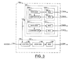
- the port 106 a generally comprises a generator and compare logic block (or circuit) 120 and a control block (or circuit) 122 .
- the generation and compare logic block 120 may be implemented as a local BIST generator and compare logic block.
- the control block 122 may be implemented as a local BIST control circuit.
- the control circuit 122 may have an input 124 that may receive the signal ACCESS.
- the control circuit 122 may have an input/output 126 that may present a number of signals to an input/output 128 of the generator and compare logic block 120 .
- control circuit 122 may have an output 130 that may present a signal to the output 112 a 2 of the port 106 a .
- the generator and comparator logic circuit 120 may have an input/output 132 that may present a number of signals to the input/output 112 a 1 of the port 106 a .
- the input/output 112 a 1 may be connected to the input/output 114 a 1 of the memory 104 and the output 112 a 2 may be connected to the input 114 a 2 of the memory 104 .
- the control circuit 122 may comprise a control circuit 180 , an address generator circuit 182 and a register 184 .
- the control block 122 may be implemented as a port specific BIST control circuit.
- the control circuit 180 may be implemented as a built in self test BIST circuit.
- the BIST control circuit 180 may receive the signal ACCESS.
- the BIST control circuit 180 may also present/receive the signals to/from the generation and comparator logic block 120 via input/output 126 .
- the signal ACCESS may be implemented, in one example, as a multi-bit signal. In a particular example, for a quad-port RAM, the signal ACCESS may be implemented as a 4-bit signal.
- the particular bit width of the signal ACCESS may vary depending on a particular implementation of the BIST control circuit 180 .
- the particular bit-width of the signal ACCESS does not necessarily vary as a function of the number of ports. However, in particular implementations, the number of bits of the signal ACCESS may match the number of ports.
- the BIST control circuit 180 may present a signal to the address generation block 182 .
- the address generation block 182 may be implemented, in one example, as a local BIST address generator.
- the address generation block 182 may present a signal to the register 184 .
- the register 184 may present a signal to the output 112 a 2 of the port 106 a.
- the generator and comparator circuit 120 may comprise a number of local BIST circuits 150 a - 150 n and a number of register blocks 152 a - 152 n .
- the generator and comparator logic block 120 may be implemented as a port specific BIST data generation and comparison circuit.
- Each of the local BIST circuits 150 a - 150 n generally comprises a data generation block 154 and a comparator 156 .
- the data generator block 154 may be implemented as a local BIST data generator block and the comparator 150 may be implemented as a local BIST comparator.
- the data generation block 154 and the comparator 156 may be connected.
- Each of the register blocks 152 a - 152 n generally comprises a number of registers 158 a - 158 n .
- the data generation block 154 may be configured to present a number of signals to the register 158 a .
- the comparator 156 may be configured to receive one or more signals from the register 158 n .
- the register 158 n may be configured to receive the input 112 a 1 b .
- the register 158 n may be configured to present an output 112 a 1 a .
- the register 152 may be configured to present an output 112 a 1 c and receive an input 112 a 1 n .
- the local BIST circuit 150 n and the register block 152 n may have similar components and/or operation to the local BIST circuit 150 a and the register block 152 a.
- the circuit 100 may allow placement of the BIST address generation logic 182 next to a RAM address counter logic circuit (e.g., not shown, but part of the control circuit 122 ), placement of the BIST data generation logic 154 next to a data input register, placement of the MBIST comparator logic 156 next to a data output register and placement of the MBIST control logic 180 next to the BIST address generation logic 182 .
- a RAM address counter logic circuit e.g., not shown, but part of the control circuit 122
- placement of the BIST data generation logic 154 next to a data input register placement of the MBIST comparator logic 156 next to a data output register and placement of the MBIST control logic 180 next to the BIST address generation logic 182 .
- the circuit 100 is shown implemented as a four port RAM with port specific MBIST circuits.
- the circuit 100 is shown with a minimum bit configuration. However, the circuit 100 may be implemented with other bit configurations in order to meet the criteria of a particular implementation.
- the circuit 100 may be implemented in embedded memories or other applicable devices. In one example, the circuit 100 may run a memory test without impacting RAM access time. The circuit 100 may compare multiple BIST results. The circuit 100 may also compare the BIST results to expected values of tested circuits. The circuit 100 may provide reduce circuit complexity and size, while requiring minimal circuit routing. Additionally, the circuit 100 may allow implementation of (i) local address generation circuits (e.g., the address generator 182 ), (ii) local data generation circuitry (e.g., the data generators 154 ), (iii) local MBIST comparators (e.g., the comparators 156 ) and (iv) local MBIST controllers (e.g., the controllers 180 ).
- local address generation circuits e.g., the address generator 182
- local data generation circuitry e.g., the data generators 154
- local MBIST comparators e.g., the comparators 156
- local MBIST controllers e.g., the controllers 180
Landscapes
- Engineering & Computer Science (AREA)
- General Engineering & Computer Science (AREA)
- Physics & Mathematics (AREA)
- General Physics & Mathematics (AREA)
- Tests Of Electronic Circuits (AREA)
- For Increasing The Reliability Of Semiconductor Memories (AREA)
Abstract
Description
Claims (16)
Priority Applications (1)
| Application Number | Priority Date | Filing Date | Title |
|---|---|---|---|
| US09/592,700 US6675336B1 (en) | 2000-06-13 | 2000-06-13 | Distributed test architecture for multiport RAMs or other circuitry |
Applications Claiming Priority (1)
| Application Number | Priority Date | Filing Date | Title |
|---|---|---|---|
| US09/592,700 US6675336B1 (en) | 2000-06-13 | 2000-06-13 | Distributed test architecture for multiport RAMs or other circuitry |
Publications (1)
| Publication Number | Publication Date |
|---|---|
| US6675336B1 true US6675336B1 (en) | 2004-01-06 |
Family
ID=29737019
Family Applications (1)
| Application Number | Title | Priority Date | Filing Date |
|---|---|---|---|
| US09/592,700 Expired - Lifetime US6675336B1 (en) | 2000-06-13 | 2000-06-13 | Distributed test architecture for multiport RAMs or other circuitry |
Country Status (1)
| Country | Link |
|---|---|
| US (1) | US6675336B1 (en) |
Cited By (9)
| Publication number | Priority date | Publication date | Assignee | Title |
|---|---|---|---|---|
| US20040230255A1 (en) * | 2002-03-22 | 2004-11-18 | Dobak John D. | Splanchnic nerve stimulation for treatment of obesity |
| US20060253752A1 (en) * | 2005-05-05 | 2006-11-09 | Krishnan Gopalakrishnan P | Parallel input/output self-test circuit and method |
| US20070086253A1 (en) * | 2005-10-14 | 2007-04-19 | Gerowitz Robert G | Scanned memory testing of multi-port memory arrays |
| US7269772B1 (en) | 2004-02-23 | 2007-09-11 | Cypress Semiconductor Corporation | Method and apparatus for built-in self-test (BIST) of integrated circuit device |
| US20080112241A1 (en) * | 2006-11-10 | 2008-05-15 | Kabushiki Kaisha Toshiba | Integrated circuit device |
| US20080174317A1 (en) * | 2006-12-27 | 2008-07-24 | Hynix Semiconductor Inc. | Semiconductor device |
| US9589672B2 (en) | 2014-09-30 | 2017-03-07 | Apple Inc. | Power-aware memory self-test unit |
| CN109065093A (en) * | 2018-08-17 | 2018-12-21 | 豪威科技(上海)有限公司 | On-chip memory tests circuit and method |
| US20230393774A1 (en) * | 2022-06-01 | 2023-12-07 | Micron Technology, Inc. | Test mode state machine for a memory device |
Citations (9)
| Publication number | Priority date | Publication date | Assignee | Title |
|---|---|---|---|---|
| US5258986A (en) * | 1990-09-19 | 1993-11-02 | Vlsi Technology, Inc. | Tightly coupled, low overhead RAM built-in self-test logic with particular applications for embedded memories |
| US5301199A (en) * | 1991-12-16 | 1994-04-05 | Nippon Telegraph And Telephone Corporation | Built-in self test circuit |
| US5377200A (en) * | 1992-08-27 | 1994-12-27 | Advanced Micro Devices, Inc. | Power saving feature for components having built-in testing logic |
| US5764655A (en) * | 1997-07-02 | 1998-06-09 | International Business Machines Corporation | Built in self test with memory |
| US5796745A (en) * | 1996-07-19 | 1998-08-18 | International Business Machines Corporation | Memory array built-in self test circuit for testing multi-port memory arrays |
| US5862151A (en) * | 1997-01-23 | 1999-01-19 | Unisys Corporation | Array self-test fault tolerant programmable threshold algorithm |
| US6067262A (en) * | 1998-12-11 | 2000-05-23 | Lsi Logic Corporation | Redundancy analysis for embedded memories with built-in self test and built-in self repair |
| US6216241B1 (en) * | 1998-10-08 | 2001-04-10 | Agere Systems Guardian Corp. | Method and system for testing multiport memories |
| US6311300B1 (en) * | 1998-06-16 | 2001-10-30 | Mitsubishi Denki Kabushiki Kaisha | Semiconductor testing apparatus for testing semiconductor device including built in self test circuit |
-
2000
- 2000-06-13 US US09/592,700 patent/US6675336B1/en not_active Expired - Lifetime
Patent Citations (9)
| Publication number | Priority date | Publication date | Assignee | Title |
|---|---|---|---|---|
| US5258986A (en) * | 1990-09-19 | 1993-11-02 | Vlsi Technology, Inc. | Tightly coupled, low overhead RAM built-in self-test logic with particular applications for embedded memories |
| US5301199A (en) * | 1991-12-16 | 1994-04-05 | Nippon Telegraph And Telephone Corporation | Built-in self test circuit |
| US5377200A (en) * | 1992-08-27 | 1994-12-27 | Advanced Micro Devices, Inc. | Power saving feature for components having built-in testing logic |
| US5796745A (en) * | 1996-07-19 | 1998-08-18 | International Business Machines Corporation | Memory array built-in self test circuit for testing multi-port memory arrays |
| US5862151A (en) * | 1997-01-23 | 1999-01-19 | Unisys Corporation | Array self-test fault tolerant programmable threshold algorithm |
| US5764655A (en) * | 1997-07-02 | 1998-06-09 | International Business Machines Corporation | Built in self test with memory |
| US6311300B1 (en) * | 1998-06-16 | 2001-10-30 | Mitsubishi Denki Kabushiki Kaisha | Semiconductor testing apparatus for testing semiconductor device including built in self test circuit |
| US6216241B1 (en) * | 1998-10-08 | 2001-04-10 | Agere Systems Guardian Corp. | Method and system for testing multiport memories |
| US6067262A (en) * | 1998-12-11 | 2000-05-23 | Lsi Logic Corporation | Redundancy analysis for embedded memories with built-in self test and built-in self repair |
Cited By (16)
| Publication number | Priority date | Publication date | Assignee | Title |
|---|---|---|---|---|
| US20040230255A1 (en) * | 2002-03-22 | 2004-11-18 | Dobak John D. | Splanchnic nerve stimulation for treatment of obesity |
| US7269772B1 (en) | 2004-02-23 | 2007-09-11 | Cypress Semiconductor Corporation | Method and apparatus for built-in self-test (BIST) of integrated circuit device |
| US20060253752A1 (en) * | 2005-05-05 | 2006-11-09 | Krishnan Gopalakrishnan P | Parallel input/output self-test circuit and method |
| US7447958B2 (en) | 2005-05-05 | 2008-11-04 | Cypress Semiconductor Corporation | Parallel input/output self-test circuit and method |
| US20090116323A1 (en) * | 2005-10-14 | 2009-05-07 | International Business Machines Corporation | Scanned memory testing of multi-port memory arrays |
| US20070086253A1 (en) * | 2005-10-14 | 2007-04-19 | Gerowitz Robert G | Scanned memory testing of multi-port memory arrays |
| US7865786B2 (en) | 2005-10-14 | 2011-01-04 | International Business Machines Corporation | Scanned memory testing of multi-port memory arrays |
| US7506225B2 (en) | 2005-10-14 | 2009-03-17 | International Business Machines Corporation | Scanned memory testing of multi-port memory arrays |
| US20080112241A1 (en) * | 2006-11-10 | 2008-05-15 | Kabushiki Kaisha Toshiba | Integrated circuit device |
| US7783942B2 (en) | 2006-11-10 | 2010-08-24 | Kabushiki Kaisha Toshiba | Integrated circuit device with built-in self test (BIST) circuit |
| US7855570B2 (en) * | 2006-12-27 | 2010-12-21 | Hynix Semiconductor Inc. | Semiconductor device for performing mount test in response to internal test mode signals |
| US20080174317A1 (en) * | 2006-12-27 | 2008-07-24 | Hynix Semiconductor Inc. | Semiconductor device |
| US9589672B2 (en) | 2014-09-30 | 2017-03-07 | Apple Inc. | Power-aware memory self-test unit |
| CN109065093A (en) * | 2018-08-17 | 2018-12-21 | 豪威科技(上海)有限公司 | On-chip memory tests circuit and method |
| US20230393774A1 (en) * | 2022-06-01 | 2023-12-07 | Micron Technology, Inc. | Test mode state machine for a memory device |
| US12210766B2 (en) * | 2022-06-01 | 2025-01-28 | Micron Technology, Inc. | Test mode state machine for a memory device |
Similar Documents
| Publication | Publication Date | Title |
|---|---|---|
| US6560740B1 (en) | Apparatus and method for programmable built-in self-test and self-repair of embedded memory | |
| US4736373A (en) | Memory tester having concurrent failure data readout and memory repair analysis | |
| US6581174B2 (en) | On-chip testing circuit and method for integrated circuits | |
| US4460999A (en) | Memory tester having memory repair analysis under pattern generator control | |
| US7225379B2 (en) | Circuit and method for testing semiconductor device | |
| KR20010037848A (en) | Semiconductor memory device and parallel bit test method thereof | |
| US6675336B1 (en) | Distributed test architecture for multiport RAMs or other circuitry | |
| JPH09293400A (en) | Parallel test circuit for semiconductor memory device | |
| US6256243B1 (en) | Test circuit for testing a digital semiconductor circuit configuration | |
| US6907385B2 (en) | Memory defect redress analysis treating method, and memory testing apparatus performing the method | |
| US6035431A (en) | Semiconductor integrated circuit with test device | |
| KR100200481B1 (en) | Test circuit | |
| JPH10106292A (en) | Memory tester | |
| US7117394B2 (en) | Built-in self-test circuit | |
| US6327683B1 (en) | Device scan testing | |
| US6675337B1 (en) | Built-in self verification circuit for system chip design | |
| US6463562B1 (en) | Semiconductor device including macros and its testing method | |
| US7230861B2 (en) | Semiconductor integrated circuit | |
| EP1763677B1 (en) | Circuit arrangement and method of testing an application circuit provided in said circuit arrangement | |
| US7318182B2 (en) | Memory array manufacturing defect detection system and method | |
| JP3516834B2 (en) | Semiconductor integrated circuit | |
| JP2007272982A (en) | Semiconductor memory device and inspection method thereof | |
| KR100491052B1 (en) | Testing circuit for SoC and method of testing the SoC | |
| JPH08184645A (en) | Semiconductor integrated circuit and test method therefor | |
| JP2002243801A (en) | Semiconductor integrated circuit |
Legal Events
| Date | Code | Title | Description |
|---|---|---|---|
| AS | Assignment |
Owner name: CYPRESS SEMICONDUCTOR CORPORATION, CALIFORNIA Free format text: ASSIGNMENT OF ASSIGNORS INTEREST;ASSIGNORS:NARAYANA, PIDUGU L.;THAKUR, SANGEETA;HAMADEH, EMAD;REEL/FRAME:010864/0453;SIGNING DATES FROM 20000602 TO 20000612 |
|
| STCF | Information on status: patent grant |
Free format text: PATENTED CASE |
|
| FPAY | Fee payment |
Year of fee payment: 4 |
|
| FPAY | Fee payment |
Year of fee payment: 8 |
|
| AS | Assignment |
Owner name: MORGAN STANLEY SENIOR FUNDING, INC., NEW YORK Free format text: SECURITY INTEREST;ASSIGNORS:CYPRESS SEMICONDUCTOR CORPORATION;SPANSION LLC;REEL/FRAME:035240/0429 Effective date: 20150312 |
|
| FPAY | Fee payment |
Year of fee payment: 12 |
|
| AS | Assignment |
Owner name: SPANSION LLC, CALIFORNIA Free format text: PARTIAL RELEASE OF SECURITY INTEREST IN PATENTS;ASSIGNOR:MORGAN STANLEY SENIOR FUNDING, INC., AS COLLATERAL AGENT;REEL/FRAME:039708/0001 Effective date: 20160811 Owner name: CYPRESS SEMICONDUCTOR CORPORATION, CALIFORNIA Free format text: PARTIAL RELEASE OF SECURITY INTEREST IN PATENTS;ASSIGNOR:MORGAN STANLEY SENIOR FUNDING, INC., AS COLLATERAL AGENT;REEL/FRAME:039708/0001 Effective date: 20160811 |
|
| AS | Assignment |
Owner name: MONTEREY RESEARCH, LLC, CALIFORNIA Free format text: ASSIGNMENT OF ASSIGNORS INTEREST;ASSIGNOR:CYPRESS SEMICONDUCTOR CORPORATION;REEL/FRAME:040911/0238 Effective date: 20160811 |
|
| AS | Assignment |
Owner name: MORGAN STANLEY SENIOR FUNDING, INC., NEW YORK Free format text: CORRECTIVE ASSIGNMENT TO CORRECT THE 8647899 PREVIOUSLY RECORDED ON REEL 035240 FRAME 0429. ASSIGNOR(S) HEREBY CONFIRMS THE SECURITY INTERST;ASSIGNORS:CYPRESS SEMICONDUCTOR CORPORATION;SPANSION LLC;REEL/FRAME:058002/0470 Effective date: 20150312 |