US6630822B2 - MR angle sensor - Google Patents
MR angle sensor Download PDFInfo
- Publication number
- US6630822B2 US6630822B2 US09/817,109 US81710901A US6630822B2 US 6630822 B2 US6630822 B2 US 6630822B2 US 81710901 A US81710901 A US 81710901A US 6630822 B2 US6630822 B2 US 6630822B2
- Authority
- US
- United States
- Prior art keywords
- strip
- shaped
- magnetic field
- elements
- sensor elements
- Prior art date
- Legal status (The legal status is an assumption and is not a legal conclusion. Google has not performed a legal analysis and makes no representation as to the accuracy of the status listed.)
- Expired - Fee Related, expires
Links
- 229910001030 Iron–nickel alloy Inorganic materials 0.000 claims abstract description 34
- 239000000463 material Substances 0.000 claims abstract description 10
- 230000005415 magnetization Effects 0.000 abstract description 11
- 238000005259 measurement Methods 0.000 abstract description 8
- 230000009467 reduction Effects 0.000 abstract description 6
- 230000008859 change Effects 0.000 abstract description 4
- 230000000694 effects Effects 0.000 abstract description 3
- 238000004519 manufacturing process Methods 0.000 description 3
- 239000011149 active material Substances 0.000 description 2
- 238000002465 magnetic force microscopy Methods 0.000 description 2
- 239000004065 semiconductor Substances 0.000 description 2
- 235000013290 Sagittaria latifolia Nutrition 0.000 description 1
- 230000008901 benefit Effects 0.000 description 1
- 235000015246 common arrowhead Nutrition 0.000 description 1
- 230000001143 conditioned effect Effects 0.000 description 1
- 239000013078 crystal Substances 0.000 description 1
- 230000001419 dependent effect Effects 0.000 description 1
- 238000009413 insulation Methods 0.000 description 1
- 239000002184 metal Substances 0.000 description 1
- 230000004048 modification Effects 0.000 description 1
- 238000012986 modification Methods 0.000 description 1
- 238000005457 optimization Methods 0.000 description 1
- 229910000889 permalloy Inorganic materials 0.000 description 1
- 238000000206 photolithography Methods 0.000 description 1
Images


Classifications
-
- G—PHYSICS
- G01—MEASURING; TESTING
- G01R—MEASURING ELECTRIC VARIABLES; MEASURING MAGNETIC VARIABLES
- G01R33/00—Arrangements or instruments for measuring magnetic variables
- G01R33/02—Measuring direction or magnitude of magnetic fields or magnetic flux
- G01R33/06—Measuring direction or magnitude of magnetic fields or magnetic flux using galvano-magnetic devices
- G01R33/09—Magnetoresistive devices
Definitions
- the invention relates to magnetoresistive sensors for angle measurements.
- a preferred field of application of magnetoresistive sensors is their use for contactless angle measurement.
- Magnetoresistive sensors for angle measurements such as, for example, the sensors of the type KMZ 41, manufactured and marketed by Philips Semiconductors, are principally known and utilize the magnetoresistive effect.
- a preferred use of MR sensors is in the weak field, angle and rotation measurements and in Magnetic Force Microscopy measurements (abbreviated MFM measurements; for example, on crystals of the product marketed as KMZB34 by Philips Semiconductors).
- Magnetoresistive sensors for angle measurements operate in the saturation range, i.e. they utilize the effect that a sufficiently strong external magnetic field H rotates an internal magnetization M of the sensor elements in the arrangement of the magnetoresistive sensor in a (substantially) fully parallel direction.
- the magnetic field strength of the external magnetic field required for full alignment of the internal magnetization is 70 to 100 kA/m. The generation of such a strong magnetic field requires a relatively high number of constructive components. A reduction of this high field strength is desirable.
- a magnetic field-sensitive sensor arrangement comprising at least a sensor element of NiFe material arranged substantially in a plane and being substantially strip-shaped in this plane, which sensor element has a contour in this plane which comprises substantially a central area with mutually parallel boundary lines, and, at least at one of the ends of the central area, an end segment which is at least substantially bounded by elliptical curves and/or is tapered towards the end.
- the magnetic field-sensitive sensor arrangement according to the invention is thus distinguished by shape-optimized, strip-shaped thin layers of a magneto-resistive material, preferably permalloy or NiFe 81:19.
- the desirable decrease of said high field strengths can be achieved by increasing the tendency of the internal magnetization to change its direction.
- An increase of the tendency of the internal magnetization to change its alignment is achieved, according to the invention, by strip-shaped sensor elements of NiFe material having elliptical contours or tapered ends.
- the rotatability of the magnetization is enhanced in the magnetic field-sensitive sensor arrangement according to the invention by giving the MR sensor elements a suitable shape.
- a circular MR structure provides the principally easiest rotatability of the magnetization. It is therefore obvious to realize the sensor elements also in a circular shape. However, this has the drawback that—conditioned by manufacturing spreads (mask adjustment in photolithography, etc.)—such circular structures can only be contacted incompletely, i.e. with high tolerances, and, moreover, require a large surface area.
- the invention is based on the recognition that MR structures utilizing elliptical and circular geometries in a defined way have a far better rotatability of the magnetization than the typically used rectangular structures. In this respect it is important that elliptical structures with pointed corners have a very weak domain splitting. By combination with rectangular parts of the MR strips, these structures can nevertheless be manufactured in a satisfactorily reproducible way while maintaining typical manufacturing tolerances.
- the invention has the advantage of a reduction, which is comparably easy to realize, of the required saturation field strength to 20-30 kA/m at a small angle error by shape anisotropy.
- the reduction of the saturation field strength is supported by using very thin layers, while the reduction of the shape anisotropy is achieved by the shape optimization of the strips according to the invention.
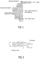
- FIG. 1 shows diagrammatically a magnetic field-sensitive sensor arrangement with a plurality of sensor elements of NiFe material which are arranged substantially in a plane and are substantially strip-shaped in this plane, which elements constitute a strip-shaped meandering NiFe structure in which the separate sensor elements are interconnected by NiFe strip terminations.
- WTi—Al short-circuits additionally connect the ends of the sensor elements in the form of a meander and the overall arrangement has external contacts by means of WTi—Al leads.
- FIG. 2 shows diagrammatically a first embodiment of a sensor element according to the invention.
- all NiFe strips are constituted by the combination of two basic shapes: a rectangular strip and an NiFe termination. All combinations of “NiFe termination” of a rectangular strip and “NiFe short-circuit” are possible in accordance with the invention.
- the length of the peak l is an n-fold value, n ⁇ , of the strip width b. There is at least substantially no curvature of the lateral contours of the end segments.
- the length of the peak l is an m-fold value, m ⁇ , of the strip width b.
- the curvature of the “arrow head” corresponds to the cut-set of one or two ellipses.
- the length of the long semi-axis is the h-fold value, with h ⁇ of the strip width b (h>b), in which the distance x between the vortex of the ellipse and the end of the rectangular strip part must not become negative.
- FIG. 4 shows the arrangement of the NiFe structures in the magnetic field-sensitive sensor arrangement which is commercially available as type KMZ 51.
- FIG. 5 shows a first embodiment of an NiFe short-circuit according to the invention.
- the width of the short-circuit strip j is smaller than or equal to the NiFe strip width b.
- Any non-magnetizable or magnetically active material or any comparable material combination such as, for example, alu on WTi may be used as a material for the short-circuit strip.
- FIG. 6 shows a modification of an NiFe short circuit according to the invention with a short-circuit strip which is distinguished in that a contact metal connection represents a small-area (circular or rectangular) contact with the first NiFe structure and subsequently extends—separated by an insulation layer of NiFe—to the second NiFe structure so as to contact this structure also on a small area. Fluctuations of the sensor resistance, conditioned by adjusting tolerances in the manufacturing process, are thus reduced.
- Any non-magnetizable or magnetically active material or a corresponding material combination, for example alu on WTi may be used as a material for the short-circuit strip.
- FIG. 7 shows a further embodiment of an NiFe short-circuit according to the invention. It comprises a superposed NiFe circle whose center is located exactly between two adjacent strips and whose diameter is defined by the fact that the current density in the short circuit does not exceed 10 7 A/cm 2 .
- the width of the strips and the diameter are preferably dimensioned substantially identically. Instead of a circle, ellipses of any ratio from the short to the long semi-axis may be used.
- FIG. 8 shows a further embodiment of an NiFe short circuit according to the invention which, in accordance with its contour, is also denoted as NiFe short circuit “gothic”.
- the connection of the NiFe strips is defined by the inserted areas of four ellipses conforming to adjacent NiFe strips on the inner and outer side, i.e. the curvature of the “gothic peak” is described by these four ellipses.
- These ellipses are combined to two pairs of ellipses, with two ellipses forming the outer side of the “gothic peak” (first pair of ellipses) and two further ellipses constitute the inner side of the “gothic peak” (second pair of ellipses).
- the dimensions of the ellipses of a pair of ellipses are identical. It holds for the outer pair of ellipses that the length of their short semi-axis is the g-fold value of the strip width b, with each ellipse conforming to one side of the strip and g being a number larger than 1. The length of the long semi-axis of the outer pair of ellipses is the h-fold value of the strip width b, in which h is a number larger than 1 and the distance x between the vortex of the ellipse and the end of the rectangular strip part does not become negative. The same holds for the inner pair of ellipses, except that g and h may also be smaller than 1.
- connection of the adjacent NiFe strips is constituted by a single arc of a circle as a special case of the “gothic peak”.
- the presence of a sharp “gothic peak” leads of course to a smaller domain splitting and is therefore preferable.
- NiFe structures are described hereinafter, which are constituted by the combination of a circular basic shape and an arbitrary NiFe short circuit, as described hereinbefore.
- a preferred embodiment is the combination with an NiFe short circuit as shown in FIG. 6 .
- FIG. 9 shows an NiFe structure in the form of a circle with diameter b.
- FIG. 10 shows an elliptical NiFe structure with a length of the semi-axes of a/2 and b/2, in which a>b and a, b ⁇ .
- This NiFe structure is usable preferably in connection with an NiFe termination as shown in FIGS. 2 and 3.
Landscapes
- Physics & Mathematics (AREA)
- Condensed Matter Physics & Semiconductors (AREA)
- General Physics & Mathematics (AREA)
- Hall/Mr Elements (AREA)
Abstract
Description
Claims (11)
Applications Claiming Priority (3)
| Application Number | Priority Date | Filing Date | Title |
|---|---|---|---|
| DE10014779 | 2000-03-27 | ||
| DE10014779.8 | 2000-03-27 | ||
| DE10014779A DE10014779B4 (en) | 2000-03-27 | 2000-03-27 | MR angle sensor |
Publications (2)
| Publication Number | Publication Date |
|---|---|
| US20010030540A1 US20010030540A1 (en) | 2001-10-18 |
| US6630822B2 true US6630822B2 (en) | 2003-10-07 |
Family
ID=7636279
Family Applications (1)
| Application Number | Title | Priority Date | Filing Date |
|---|---|---|---|
| US09/817,109 Expired - Fee Related US6630822B2 (en) | 2000-03-27 | 2001-03-26 | MR angle sensor |
Country Status (2)
| Country | Link |
|---|---|
| US (1) | US6630822B2 (en) |
| DE (1) | DE10014779B4 (en) |
Families Citing this family (1)
| Publication number | Priority date | Publication date | Assignee | Title |
|---|---|---|---|---|
| JP6583208B2 (en) * | 2016-10-14 | 2019-10-02 | 株式会社デンソー | Magnetic detection element |
Citations (6)
| Publication number | Priority date | Publication date | Assignee | Title |
|---|---|---|---|---|
| US4847584A (en) * | 1988-10-14 | 1989-07-11 | Honeywell Inc. | Magnetoresistive magnetic sensor |
| US5247278A (en) * | 1991-11-26 | 1993-09-21 | Honeywell Inc. | Magnetic field sensing device |
| US5602471A (en) * | 1994-03-10 | 1997-02-11 | U.S. Philips Corporation | Angle sensor including angularly spaced sensor units |
| US5684397A (en) * | 1994-12-07 | 1997-11-04 | Nec Corporation | Magnetoresistive sensor |
| US5820924A (en) * | 1996-05-16 | 1998-10-13 | Honeywell Inc. | Method of fabricating a magnetoresistive sensor |
| US6222361B1 (en) * | 1997-12-04 | 2001-04-24 | Sony Precision Technology Inc. | Position detecting device using varying width magneto-resistive effect sensor |
Family Cites Families (6)
| Publication number | Priority date | Publication date | Assignee | Title |
|---|---|---|---|---|
| US4841398A (en) * | 1987-02-17 | 1989-06-20 | Magnetic Peripherals Inc. | Non linear magnetoresistive sensor |
| US4967298A (en) * | 1987-02-17 | 1990-10-30 | Mowry Greg S | Magnetic head with magnetoresistive sensor, inductive write head, and shield |
| US5351028A (en) * | 1993-06-14 | 1994-09-27 | Honeywell Inc. | Magnetoresistive proximity sensor |
| DE4327458C2 (en) * | 1993-08-16 | 1996-09-05 | Inst Mikrostrukturtechnologie | Sensor chip for high-resolution measurement of the magnetic field strength |
| DE19740408A1 (en) * | 1996-09-09 | 1998-03-12 | H Schiebel Elektronische Gerae | Magnetic field sensor |
| DE19648879C2 (en) * | 1996-11-26 | 2000-04-13 | Inst Mikrostrukturtechnologie | Magnetic field sensor with parallel magnetoresistive layer strips |
-
2000
- 2000-03-27 DE DE10014779A patent/DE10014779B4/en not_active Expired - Fee Related
-
2001
- 2001-03-26 US US09/817,109 patent/US6630822B2/en not_active Expired - Fee Related
Patent Citations (6)
| Publication number | Priority date | Publication date | Assignee | Title |
|---|---|---|---|---|
| US4847584A (en) * | 1988-10-14 | 1989-07-11 | Honeywell Inc. | Magnetoresistive magnetic sensor |
| US5247278A (en) * | 1991-11-26 | 1993-09-21 | Honeywell Inc. | Magnetic field sensing device |
| US5602471A (en) * | 1994-03-10 | 1997-02-11 | U.S. Philips Corporation | Angle sensor including angularly spaced sensor units |
| US5684397A (en) * | 1994-12-07 | 1997-11-04 | Nec Corporation | Magnetoresistive sensor |
| US5820924A (en) * | 1996-05-16 | 1998-10-13 | Honeywell Inc. | Method of fabricating a magnetoresistive sensor |
| US6222361B1 (en) * | 1997-12-04 | 2001-04-24 | Sony Precision Technology Inc. | Position detecting device using varying width magneto-resistive effect sensor |
Also Published As
| Publication number | Publication date |
|---|---|
| US20010030540A1 (en) | 2001-10-18 |
| DE10014779B4 (en) | 2011-11-10 |
| DE10014779A1 (en) | 2001-10-11 |
Similar Documents
| Publication | Publication Date | Title |
|---|---|---|
| JP6003968B2 (en) | Magnetic field detection device and current sensor | |
| JP3017061B2 (en) | Bridge circuit magnetic field sensor | |
| EP3223028B1 (en) | Multiple axis magnetic sensor | |
| US6556007B1 (en) | Bearing sensor having magneto resistive elements | |
| GB2052855A (en) | Magnetoresistive transducers | |
| JPH11513128A (en) | Magnetic field sensor with magnetoresistive bridge | |
| JPH11194161A (en) | Sensor for detecting orientation of external field through a reluctance sensor element | |
| US9678176B2 (en) | XMR angle sensors | |
| JPH11505966A (en) | Magnetic field sensor with bridge circuit of magnetoresistive bridge element | |
| US7176679B2 (en) | Sensor structure and magnetic field sensor | |
| JP2005502052A (en) | Three-dimensional strap for magnetoresistive sensors | |
| JP2000512763A (en) | Magnetic field sensor with Wheatstone bridge | |
| US6630822B2 (en) | MR angle sensor | |
| CN100429799C (en) | Magnetic inductor and its manufacturing method | |
| US6727694B2 (en) | MR angle sensor | |
| JP4404069B2 (en) | Magnetic sensor | |
| CN108363025B (en) | magnetic field sensor | |
| JP2576763B2 (en) | Ferromagnetic magnetoresistive element | |
| JPH0563254A (en) | Magnetoresistance composite element | |
| JPS6034048B2 (en) | displacement detection device | |
| JP3555412B2 (en) | Magnetoresistive sensor | |
| JP3067278B2 (en) | Magnetic sensor | |
| JPH01227482A (en) | Magneto-resistive element | |
| JPH07249808A (en) | Magnetoelectric conversion element | |
| RU1764423C (en) | Process of manufacture of magnetosensitive strip element on base of thin-film composite magnetoresistive material |
Legal Events
| Date | Code | Title | Description |
|---|---|---|---|
| AS | Assignment |
Owner name: U.S. PHILIPS CORPORATION, NEW YORK Free format text: ASSIGNMENT OF ASSIGNORS INTEREST;ASSIGNOR:DOESCHER, MICHAEL;REEL/FRAME:011875/0859 Effective date: 20010417 |
|
| AS | Assignment |
Owner name: KONINKLIJKE PHILIPS ELECTRONICS N.V., NETHERLANDS Free format text: ASSIGNMENT OF ASSIGNORS INTEREST;ASSIGNOR:U. S. PHILIPS CORPORATION;REEL/FRAME:014361/0868 Effective date: 20030715 |
|
| AS | Assignment |
Owner name: NXP B.V., NETHERLANDS Free format text: ASSIGNMENT OF ASSIGNORS INTEREST;ASSIGNOR:KONINKLIJKE PHILIPS ELECTRONICS N.V.;REEL/FRAME:018635/0787 Effective date: 20061117 |
|
| AS | Assignment |
Owner name: MORGAN STANLEY SENIOR FUNDING, INC., ENGLAND Free format text: SECURITY AGREEMENT;ASSIGNOR:NXP B.V.;REEL/FRAME:018806/0201 Effective date: 20061201 |
|
| FPAY | Fee payment |
Year of fee payment: 4 |
|
| FPAY | Fee payment |
Year of fee payment: 8 |
|
| REMI | Maintenance fee reminder mailed | ||
| LAPS | Lapse for failure to pay maintenance fees | ||
| STCH | Information on status: patent discontinuation |
Free format text: PATENT EXPIRED DUE TO NONPAYMENT OF MAINTENANCE FEES UNDER 37 CFR 1.362 |
|
| FP | Lapsed due to failure to pay maintenance fee |
Effective date: 20151007 |
|
| AS | Assignment |
Owner name: NXP B.V., NETHERLANDS Free format text: RELEASE BY SECURED PARTY;ASSIGNOR:MORGAN STANLEY SENIOR FUNDING, INC;REEL/FRAME:050315/0443 Effective date: 20190903 |