US6556063B2 - Fast transmission gate switch - Google Patents
Fast transmission gate switch Download PDFInfo
- Publication number
- US6556063B2 US6556063B2 US09/772,448 US77244801A US6556063B2 US 6556063 B2 US6556063 B2 US 6556063B2 US 77244801 A US77244801 A US 77244801A US 6556063 B2 US6556063 B2 US 6556063B2
- Authority
- US
- United States
- Prior art keywords
- transistor
- input
- output
- lead
- switch
- Prior art date
- Legal status (The legal status is an assumption and is not a legal conclusion. Google has not performed a legal analysis and makes no representation as to the accuracy of the status listed.)
- Expired - Fee Related
Links
Images


Classifications
-
- H—ELECTRICITY
- H03—ELECTRONIC CIRCUITRY
- H03K—PULSE TECHNIQUE
- H03K17/00—Electronic switching or gating, i.e. not by contact-making and –breaking
- H03K17/51—Electronic switching or gating, i.e. not by contact-making and –breaking characterised by the components used
- H03K17/56—Electronic switching or gating, i.e. not by contact-making and –breaking characterised by the components used by the use, as active elements, of semiconductor devices
- H03K17/687—Electronic switching or gating, i.e. not by contact-making and –breaking characterised by the components used by the use, as active elements, of semiconductor devices the devices being field-effect transistors
- H03K17/693—Switching arrangements with several input- or output-terminals, e.g. multiplexers, distributors
-
- H—ELECTRICITY
- H03—ELECTRONIC CIRCUITRY
- H03K—PULSE TECHNIQUE
- H03K17/00—Electronic switching or gating, i.e. not by contact-making and –breaking
- H03K17/04—Modifications for accelerating switching
- H03K17/041—Modifications for accelerating switching without feedback from the output circuit to the control circuit
- H03K17/04106—Modifications for accelerating switching without feedback from the output circuit to the control circuit in field-effect transistor switches
-
- H—ELECTRICITY
- H03—ELECTRONIC CIRCUITRY
- H03K—PULSE TECHNIQUE
- H03K17/00—Electronic switching or gating, i.e. not by contact-making and –breaking
- H03K17/04—Modifications for accelerating switching
- H03K17/041—Modifications for accelerating switching without feedback from the output circuit to the control circuit
- H03K17/04113—Modifications for accelerating switching without feedback from the output circuit to the control circuit in bipolar transistor switches
Definitions
- This invention relates in general to signal switches and in particular, to a fast transmission gate switch, particularly useful for switching digital logic signals.
- an active device such as a logic buffer is used. While a buffer used as a switch causes a delay that is less than that caused by the conventional passive transmission gate switch, the delay caused by such buffers may nevertheless be excessive and undesirable for some high speed applications. It is thus desirable to provide a high speed switch that causes less delay than the above described switches.
- the switching device of this invention has two input/output ports for passing or blocking signals between the two ports of the device.
- the device comprises a transistor having a first and a second terminal and a control terminal. The first and second terminals are connected between the two ports. The transistor thereby passes signals between the two ports when the transistor is turned on and blocks the passage of signals between the two ports when the transistor is turned off.
- the resistance between the first and second terminals is less than about 10 ohms when the transistor is turned on.
- the device further comprises means for applying a switching signal to the control terminal of the transistor for turning it on or off.
- the capacitance between the first or second terminal and a reference potential is less than about 50 pF when the transistor is turned on.
- FIG. 1 is a schematic circuit diagram of a passive transmission gate switch illustrating a conventional design.
- FIG. 2 is a schematic view of an active switch device using an enabled buffer to illustrate another conventional design.
- FIG. 3 is a perspective view of a MOS transistor useful for illustrating the invention.
- FIG. 4 is a cross-sectional view of the transistor of FIG. 3 .
- FIG. 5 is a schematic circuit diagram of a transmission gate switch and of a driver and receiver to illustrate the Preferred embodiment of the invention.
- FIG. 6 is a schematic circuit diagram of a transmission gate switch and of a driver and receiver to illustrate an alternative embodiment of the invention.
- FIGS. 7 and 8 are schematic circuit diagrams of two different transmission gate switches to illustrate additional alternative embodiments of the invention.
- FIG. 9 is a schematic view of a bus switch for switching signals between two sets of bus lines to illustrate applications of the invention.
- FIG. 10 is a schematic circuit diagram of a bus exchange switch to illustrate applications of the invention.
- FIGS. 11A, 11 B are schematic circuit diagrams illustrating the operation of the circuit in FIG. 5 .
- FIG. 12A is a block diagram of a computer system illustrating the applications of the invention.
- FIG. 12B is a timing diagram illustrating the operation of the system in FIG. 12 A.
- FIG. 1 is a schematic circuit diagram of a conventional transmission gate switch 20 connected to the output of a driver 22 and the input of a receiver 24 at nodes A, B respectively.
- the signal to be switched appears at the output of driver 22 .
- switch 20 connects nodes A and B, such signal is transmitted to node B and appears at the input of receiver 24 .
- Driver 22 and receiver 24 may each be part of another circuit chip package mounted on a printed circuit board where switch 20 is connected by conductive traces through nodes A, B to these chip packages.
- Switch 20 has resistance R so that the switch may be represented conceptually as a resistor 26 in series with a pure switch 28 as shown in FIG. 1 .
- the conductive traces 32 connecting switch 20 to driver 22 and receiver 24 have inherent capacitances and so does receiver 24 as seen by a signal propagating between nodes A and B.
- the transmission gate switch 20 itself also has capacitance.
- the total capacitance of the conductive traces, receiver 24 and switch 20 as seen by a signal propagating from A to B is commonly known as the stray capacitance and is represented conceptually as capacitor 30 in FIG. 1 .
- a measure of the delay of the signal propagating from node A to node B is given by the RC time constant, or the product of the resistance of resistor 26 and the capacitance of capacitor 30 .
- a typical stray capacitance value exclusive of the effect of the switch itself is about 50 pF. Therefore, if switch 20 has a large resistance value, the RC time constant will be large, resulting in a significant signal delay when the signal propagates from A to B.
- a standard transmission gate switch is CMOS 4016 integrated circuit.
- the typical resistance values of existing transmission gate switches such as the 4016 are in the range of 100-1,000 ohms. This type of switches would therefore introduce a delay of the order of 50-500 nanoseconds, assuming a 50 pF stray capacitance. Such delay is unacceptable for switching high speed signals required in many computer and logic applications.
- transmission gate switch 20 has been replaced by a logic buffer 40 in FIG. 2 .
- Driver 22 and receiver 24 may be part of computer or logic chip packages mounted on a printed circuit board and connected to buffer 40 by conductive traces 32 on the board.
- Buffer 40 introduces a delay of its own because of the inherent speed limitations of active logic.
- the 74F244 buffer introduces a delay of about 6.5 nanoseconds.
- This invention is based on the observation that, by employing a transistor having low inherent resistance, the signal delay of the switch can be further reduced to a value much below that of the active buffers in FIG. 2 .
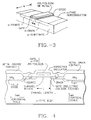
- FIG. 3 is a perspective view of a MOS transistor useful for illustrating the invention.
- FIG. 4 is a cross-sectional view of the transistor of FIG. 3 .
- the channel length of a MOS type transistor is the distance L between the source and drain regions of the transistor while the channel width is the dimension W of the transistor in the direction where the cross-sectional configuration of the transistor does not change.
- Another common definition of the channel length is the width of the gate that overlaps the active region of the transistor between the source and drain.
- Another common definition of the channel width is the length of the gate overlapping the active region of the transistor between the source and drain.
- FIG. 5 is a schematic circuit diagram of a transmission gate switch and of a driver and receiver to illustrate the preferred embodiment of the invention.
- the transmission gate 100 includes a N-channel MOS transistor 102 and a driver 104 for controlling the gate of transistor 102 in response to an external signal from node C.
- the channel length of transistor 102 is not more than 1.5 microns, preferably not more than 1 micron.
- the channel width of transistor 102 is more than about 1,000 microns and preferably 1,200 microns or more. In reference to FIGS. 3 and 4, by reducing the channel length, the resistance of the resistor is reduced since current carriers have a shorter distance to travel in order to conduct current between nodes A, B.
- the resistance of transistor 102 is further reduced in comparison.
- the inherent resistance of transmission gate switch 100 between nodes A, B when the transistor 102 is turned on can be reduced to a value of no more than 10 ohms.
- the resistance of switch 100 when transistor 102 is turned on may be reduced to a value in the range of 2-3 ohms. Shorter channel lengths also results in reduced capacitance of transistor 102 .
- a typical capacitance value of switch 100 is in the range of a few pF and is not significant compared to the typical stray capacitance of 50 pF.
- the capacitance of the transistor as seen at terminals A or B is 50 pF or less, so that the switch itself does not introduce too much of a signal delay.
- Such capacitance is, of course, measured at terminals A or B in reference to ground or another reference potential.
- the above-described transmission gate switch 100 may be used to advantageously replace active logic devices such as 74F244, 74F245 for switching high speed digital logic signals in a board level design.
- the replacement of the active device with device 100 will greatly reduce the propagation delay, logic noise (e.g., “ground bounce” noise) and power dissipation associated with the active device replaced.
- Switch 100 is also inherently bi-directional. Other embodiments of the switch described below in reference to FIGS. 5-8 also have similar advantages.
- Switch 100 may be modified by replacing transistor 102 by a P-channel transistor where the polarity of the signal for controlling the gate of the transistor has been adjusted if necessary to accommodate a P-channel device. Where the P-channel device also has the above-described channel lengths and widths, switch 100 may be constructed to have a on-resistance of not more than 10 ohms.
- the gate of transistor 102 is controlled by the output of a driver 104 which may include a pair of P-channel and N-channel resistors connected in parallel between node C and the gate of transistor 102 .
- the pair of transistors in driver 104 would preferably each have a channel length of 1.5 microns or less.
- the transistors in device 100 may be grown so that all the transistors in the device have short channel lengths.
- device 100 is fabricated as an integrated circuit, it can be made in the form of a package having three pins for connection to nodes A, B and C.
- FIG. 6 is a schematic circuit diagram of a transmission gate switch and of a driver and receiver to illustrate an alternative embodiment of the invention.
- switch 150 includes a pair of N-channel transistor 102 and a P-channel transistor 152 connected in parallel between nodes A, B.
- the gate of transistor 102 is controlled by a driver 104 as in FIG. 5 and the gate of transistor 152 is controlled by the output of driver 154 whose input is connected to the output of driver 104 .
- both transistors 102 , 152 have the channel lengths and widths as those described above for transistor 102 , the on-resistance of switch 150 would be 10 ohms or less.
- FIGS. 7 and 8 are schematic circuit diagrams of two different transmission gate switches to illustrate additional alternative embodiments of the invention.
- Bipolar transistors typically have on-resistances of less than 10 ohms so that they may be used instead of MOS transistor 102 .
- Such configuration is illustrated in switch 200 of FIG. 7 . While a npn transistor 202 is employed in switch 200 , it will be understood that a pnp type transistor may be used instead and is within the scope of the invention.
- the base of transistor 202 is controlled by the output of a driver 204 through resistor 206 .
- Driver 204 may be one of the 7400 TTL series of logic gates, such as the 74F04 gate.
- FIG. 8 a back to back connection of two npn transistors 202 and 252 are shown for switch 250 , although 2 pnp transistors may be used instead. It is known that for a bipolar transistor, unlike a MOS transistor, the current flowing between the collector and emitter is greater in one direction than the other. By placing two transistors 202 , 252 in two parallel paths and connected to nodes A, B so that each node is connected to a collector of one transistor and the emitter of the other transistor, currents will flow through the path of lesser resistance in each direction so that the amount of current that needs to be pumped through the switch is reduced.
- FIG. 9 is a schematic circuit diagram of a CMOS bus switch device employing the invention for switching the signals between two sets of bus lines.
- Quality Semiconductor, Inc. of Santa Clara, Calif., assignee of the present application has employed the present invention for bus switches such as one shown in FIG. 9 in product 74FCT3384.
- switch device 500 is a high speed TTL bus connect device. When enabled, the bus switch device directly connects two buses with the connection resistance of less than 5 ohms.
- the five lines A 0 , A 1 , A 2 , A 3 , A 4 in bus A are each connected through a transistor 102 to the bus lines B 0 , B 1 , B 2 , B 3 , B 4 respectively.
- switch device 500 includes ten switches 102 arranged as two banks of five and controlled by two different drivers. This allows switch device 500 to be used as a 10-bit switch or as a 5-bit, 2-to-1 multiplexer.
- BEA BEB B0-4 B5-9 Function H H Hi-Z Hi-Z Disconnect L H A0-4 Hi-Z Connect H L Hi-Z A5-9 Connect L L A0-4 A5-9 Connect
- Device 500 includes in essence ten switches, where each switch includes an N-channel MOS transistor driven by a CMOS gate. When the switch is enabled, the gate of the N-channel transistor is at Vcc (+5 volts) and the device is on. These devices have an on resistance of less than 5 ohms for voltages near ground and will drive in excess of 64 mA each. The resistance rises somewhat as the I/O voltage rises from a TTL low of 0.0 volts to a TTL high of 2.4 volts. In this region the A and B pins are solidly connected, and the bus switch is specified in the same manner as a TTL device over this range. As the I/O voltage rises to approximately 4.0 volts, the transistor turns off. This corresponds to a typical TTL high of 3.5 to 4.0 volts.
- FIG. 10 is a schematic circuit diagram of a CMOS bus exchange switch 600 in another product 74FCT3383.
- Switch 600 comprises two banks of ten switches arranged to gate through or exchange two banks of five signals. This allows switch 600 to be used as a 10-bit switch or as a 5-bit, two-way bus exchange device. Switch 600 is particularly useful for exchange and routing operations such as byte swap, crossbar matrices, and RAM sharing. The functions of switch 600 are summarized in the Table below.
- the bus switch provides a path for a driving device to drive capacitance to ground and to drive capacitance up from ground. This is shown in FIGS. 11A, 11 B.
- the N-channel transistor When the A (or B) input is driven to a TTL low of 0.0 volts, the N-channel transistor is fully on and the B (or A) output will follow it.
- the capacitor side of the N-channel switch is at 0.0 volts, the switch is fully on and the B (or A) output will follow it through threshold and beyond. This means that the rise and fall time characteristics and waveforms of the B (or A) output will be determined by the TTL driver, not the bus switch.
- the switch introduces insignificant propagation delay.
- the N-channel transistor gate When the bus switch is disabled, the N-channel transistor gate is at 0.0 volts, and the transistor is off.
- the A and B pins are fully isolated when the transistor is off. Leakage and capacitance is to the chip substrate (i.e., ground) rather than between input and output. This minimizes feedthrough in the off state. Because only an N-channel transistor is used, either A or B pin(s) can be taken to Vcc and above, and the device can be powered down without loading either bus.
- the bus switch can replace drivers and transceivers in systems if bus repowering is not required. Since the bus switch directly connects two buses, it provides no drive of its own but relies on the device that is driving data onto the connected buses. If the additional loading of the connected bus is small enough, there is a net gain in speed. For example, the sensitivity to loading of a driver such as the 74FCT244 is typically 2 ns/100 pF. If the connected bus adds 50 pF of loading the added delay will be 1 ns. This is much less than the 4-10 ns delay of the buffer or transceiver the bus switch replaces.
- FIG. 12A shows bus switches (labeled 3384 ) of the type in FIG. 9 used to allow the memory for a DSP slave processor to be accessed by the host processor.
- a 33 mHz TMS320C30 system is shown with a 16Kx32 SRAM as its program and data storage memory.
- the SRAM is connected to the DSP CPU by a 3384 device, allowing full speed operation while the CPU is running. This saves 10 ns over using conventional fast buffers and transceivers, i.e., 5 ns for a 244 address buffer to the SRAM and 5 ns for a 245 address transceiver from the SRAM, as shown in the timing diagrams in FIG. 12 B.
Landscapes
- Electronic Switches (AREA)
- Logic Circuits (AREA)
Abstract
A fast switching device for passing or blocking signals between two input/output ports includes a transistor having a first and a second terminal and a control terminal. The first and second terminals are connected between the two ports. The transistor passes signals between the ports when the transistor is turned on and blocks the passage of signals between the ports when the transistor is turned off. The resistance between the first and second terminals is less than about 10 ohms when the transistor is turned on. The device further includes a driver for controlling the control terminal of the transistor for turning it on or off. Preferably the capacitance between the first or second terminal and a reference potential is less than about 50 pF.
Description
This is a continuation of application Ser. No. 08/959,958 filed Oct. 24, 1997, now U.S. Pat. No. 6,215,350, which is a continuation of application Ser. No. 08/746,051 filed Nov. 6, 1996, now abandoned, which is a continuation of application Ser. No. 08/567,813 filed Dec. 6, 1995, now abandoned, which is a continuation of application Ser. No. 08/165,234 filed Dec. 10, 1993, now abandoned, which is a continuation of application Ser. No. 08/035,873 filed Mar. 23, 1993, which has issued as U.S. Pat. No. 5,289,062, which is a continuation of application Ser. No. 07/967,956 filed Oct. 27, 1992, now abandoned, which is a continuation of application Ser. No. 07/859,289, filed Mar. 25, 1992, now abandoned, which is a continuation of application Ser. No. 07/672,050 filed Mar. 18, 1991, now abandoned.
This invention relates in general to signal switches and in particular, to a fast transmission gate switch, particularly useful for switching digital logic signals.
With the advent of very large-scale integrated circuits, the size of devices manufactured has been shrinking and the speed of the devices has continually increased. Most of the efforts, however, have been directed to designs where many circuits and the connections between them are made in the same medium such as a silicon chip. Since all the circuit components being fabricated are done in the same medium, devices may be made smaller by improved techniques such as improved lithography. By reducing the sizes of the devices and the lengths of the connections between them, the speed of the device is increased due to a decrease in the inductances, resistances and capacitances of individual devices and of the connections between them.
Board level designs have not kept pace with the above-described development in very large-scale integrated circuits. Printed circuit board designs frequently have large capacitances which slow down signal propagation. Thus if two high speed logic chips are connected through a slower device, the overall speed of the system is determined by the slowest component, namely, the slow connecting device. Passive switching devices such as transmission gates have been used in printed circuit board level designs for switching signals between digital logic devices. The slow speed of this type of switches determines the speed of signal transmission even though the two logic devices may operate at much higher speeds. It is therefore desirable to provide a stand-alone switching device which is much faster than the conventional passive transmission gate.
In one type of improved switching circuits that is frequently used, instead of a passive switch, an active device such as a logic buffer is used. While a buffer used as a switch causes a delay that is less than that caused by the conventional passive transmission gate switch, the delay caused by such buffers may nevertheless be excessive and undesirable for some high speed applications. It is thus desirable to provide a high speed switch that causes less delay than the above described switches.
The switching device of this invention has two input/output ports for passing or blocking signals between the two ports of the device. The device comprises a transistor having a first and a second terminal and a control terminal. The first and second terminals are connected between the two ports. The transistor thereby passes signals between the two ports when the transistor is turned on and blocks the passage of signals between the two ports when the transistor is turned off. The resistance between the first and second terminals is less than about 10 ohms when the transistor is turned on. The device further comprises means for applying a switching signal to the control terminal of the transistor for turning it on or off. In the preferred embodiment, the capacitance between the first or second terminal and a reference potential is less than about 50 pF when the transistor is turned on.
FIG. 1 is a schematic circuit diagram of a passive transmission gate switch illustrating a conventional design.
FIG. 2 is a schematic view of an active switch device using an enabled buffer to illustrate another conventional design.
FIG. 3 is a perspective view of a MOS transistor useful for illustrating the invention.
FIG. 4 is a cross-sectional view of the transistor of FIG. 3.
FIG. 5 is a schematic circuit diagram of a transmission gate switch and of a driver and receiver to illustrate the Preferred embodiment of the invention.
FIG. 6 is a schematic circuit diagram of a transmission gate switch and of a driver and receiver to illustrate an alternative embodiment of the invention.
FIGS. 7 and 8 are schematic circuit diagrams of two different transmission gate switches to illustrate additional alternative embodiments of the invention.
FIG. 9 is a schematic view of a bus switch for switching signals between two sets of bus lines to illustrate applications of the invention.
FIG. 10 is a schematic circuit diagram of a bus exchange switch to illustrate applications of the invention.
FIGS. 11A, 11B are schematic circuit diagrams illustrating the operation of the circuit in FIG. 5.
FIG. 12A is a block diagram of a computer system illustrating the applications of the invention.
FIG. 12B is a timing diagram illustrating the operation of the system in FIG. 12A.
FIG. 1 is a schematic circuit diagram of a conventional transmission gate switch 20 connected to the output of a driver 22 and the input of a receiver 24 at nodes A, B respectively. The signal to be switched appears at the output of driver 22. When switch 20 connects nodes A and B, such signal is transmitted to node B and appears at the input of receiver 24. Driver 22 and receiver 24 may each be part of another circuit chip package mounted on a printed circuit board where switch 20 is connected by conductive traces through nodes A, B to these chip packages.
For typical printed circuit board designs, a typical stray capacitance value exclusive of the effect of the switch itself is about 50 pF. Therefore, if switch 20 has a large resistance value, the RC time constant will be large, resulting in a significant signal delay when the signal propagates from A to B. A standard transmission gate switch is CMOS 4016 integrated circuit. The typical resistance values of existing transmission gate switches such as the 4016 are in the range of 100-1,000 ohms. This type of switches would therefore introduce a delay of the order of 50-500 nanoseconds, assuming a 50 pF stray capacitance. Such delay is unacceptable for switching high speed signals required in many computer and logic applications. For this reason, the 4016 type switch is more commonly used in analog circuits and seldom in board level computer or digital logic designs. For the latter applications, active logic devices such as industry standard 74F244 buffers have been used such as shown in FIG. 2. To simplify the discussion, identical components and the figures of this application are identified by the same numerals.
As shown in FIGS. 1 and 2, transmission gate switch 20 has been replaced by a logic buffer 40 in FIG. 2. Driver 22 and receiver 24 may be part of computer or logic chip packages mounted on a printed circuit board and connected to buffer 40 by conductive traces 32 on the board. Buffer 40, however, introduces a delay of its own because of the inherent speed limitations of active logic. The 74F244 buffer introduces a delay of about 6.5 nanoseconds. Thus while using a logic buffer 40 to replace switch 20 does reduce the delay in signal transmission, it is difficult to further reduce the delay introduced by the buffer itself. It is therefore desirable to provide an improved switching device where the above-described difficulties are alleviated.
This invention is based on the observation that, by employing a transistor having low inherent resistance, the signal delay of the switch can be further reduced to a value much below that of the active buffers in FIG. 2.
FIG. 3 is a perspective view of a MOS transistor useful for illustrating the invention. FIG. 4 is a cross-sectional view of the transistor of FIG. 3. As shown in FIGS. 3 and 4, the channel length of a MOS type transistor is the distance L between the source and drain regions of the transistor while the channel width is the dimension W of the transistor in the direction where the cross-sectional configuration of the transistor does not change. Another common definition of the channel length is the width of the gate that overlaps the active region of the transistor between the source and drain. Another common definition of the channel width is the length of the gate overlapping the active region of the transistor between the source and drain.
FIG. 5 is a schematic circuit diagram of a transmission gate switch and of a driver and receiver to illustrate the preferred embodiment of the invention. As shown in FIG. 5, the transmission gate 100 includes a N-channel MOS transistor 102 and a driver 104 for controlling the gate of transistor 102 in response to an external signal from node C. The channel length of transistor 102 is not more than 1.5 microns, preferably not more than 1 micron. The channel width of transistor 102 is more than about 1,000 microns and preferably 1,200 microns or more. In reference to FIGS. 3 and 4, by reducing the channel length, the resistance of the resistor is reduced since current carriers have a shorter distance to travel in order to conduct current between nodes A, B. By using a transistor with large channel width compared to the transistors in the 4016 type gate, the resistance of transistor 102 is further reduced in comparison. With the above-described design for transistor 102, it is found that the inherent resistance of transmission gate switch 100 between nodes A, B when the transistor 102 is turned on (on-resistance) can be reduced to a value of no more than 10 ohms. Applicant has discovered that in some designs, the resistance of switch 100 when transistor 102 is turned on may be reduced to a value in the range of 2-3 ohms. Shorter channel lengths also results in reduced capacitance of transistor 102. A typical capacitance value of switch 100 is in the range of a few pF and is not significant compared to the typical stray capacitance of 50 pF. Thus, it is preferable for the capacitance of the transistor as seen at terminals A or B to be 50 pF or less, so that the switch itself does not introduce too much of a signal delay. Such capacitance is, of course, measured at terminals A or B in reference to ground or another reference potential.
The above-described transmission gate switch 100 may be used to advantageously replace active logic devices such as 74F244, 74F245 for switching high speed digital logic signals in a board level design. The replacement of the active device with device 100 will greatly reduce the propagation delay, logic noise (e.g., “ground bounce” noise) and power dissipation associated with the active device replaced. Switch 100 is also inherently bi-directional. Other embodiments of the switch described below in reference to FIGS. 5-8 also have similar advantages.
The gate of transistor 102 is controlled by the output of a driver 104 which may include a pair of P-channel and N-channel resistors connected in parallel between node C and the gate of transistor 102. In order to increase the speed of switching, the pair of transistors in driver 104 would preferably each have a channel length of 1.5 microns or less. Where a driver 104 and transistor 102 are fabricated as a stand-alone integrated circuit device 100 using the same fabrication technology, the transistors in device 100 may be grown so that all the transistors in the device have short channel lengths. Where device 100 is fabricated as an integrated circuit, it can be made in the form of a package having three pins for connection to nodes A, B and C.
FIG. 6 is a schematic circuit diagram of a transmission gate switch and of a driver and receiver to illustrate an alternative embodiment of the invention. As shown in FIG. 6, switch 150 includes a pair of N-channel transistor 102 and a P-channel transistor 152 connected in parallel between nodes A, B. The gate of transistor 102 is controlled by a driver 104 as in FIG. 5 and the gate of transistor 152 is controlled by the output of driver 154 whose input is connected to the output of driver 104. Where both transistors 102, 152 have the channel lengths and widths as those described above for transistor 102, the on-resistance of switch 150 would be 10 ohms or less.
FIGS. 7 and 8 are schematic circuit diagrams of two different transmission gate switches to illustrate additional alternative embodiments of the invention. Bipolar transistors typically have on-resistances of less than 10 ohms so that they may be used instead of MOS transistor 102. Such configuration is illustrated in switch 200 of FIG. 7. While a npn transistor 202 is employed in switch 200, it will be understood that a pnp type transistor may be used instead and is within the scope of the invention. As shown in FIG. 7, the base of transistor 202 is controlled by the output of a driver 204 through resistor 206. Driver 204 may be one of the 7400 TTL series of logic gates, such as the 74F04 gate.
In FIG. 8, a back to back connection of two npn transistors 202 and 252 are shown for switch 250, although 2 pnp transistors may be used instead. It is known that for a bipolar transistor, unlike a MOS transistor, the current flowing between the collector and emitter is greater in one direction than the other. By placing two transistors 202, 252 in two parallel paths and connected to nodes A, B so that each node is connected to a collector of one transistor and the emitter of the other transistor, currents will flow through the path of lesser resistance in each direction so that the amount of current that needs to be pumped through the switch is reduced.
FIG. 9 is a schematic circuit diagram of a CMOS bus switch device employing the invention for switching the signals between two sets of bus lines. Quality Semiconductor, Inc. of Santa Clara, Calif., assignee of the present application, has employed the present invention for bus switches such as one shown in FIG. 9 in product 74FCT3384. As shown in FIG. 9, switch device 500 is a high speed TTL bus connect device. When enabled, the bus switch device directly connects two buses with the connection resistance of less than 5 ohms. The five lines A0, A1, A2, A3, A4 in bus A are each connected through a transistor 102 to the bus lines B0, B1, B2, B3, B4 respectively. The five transistors 102 connecting A0-A4 to B0-B4 have their gates controlled by the output of driver 104′. Similarly, the five lines A5-A9 in bus A are connected to the respective one of the five bus lines B5-B9 in bus B through transistors 102 whose gates are controlled by the outputs of a driver 104″. Thus switch device 500 includes ten switches 102 arranged as two banks of five and controlled by two different drivers. This allows switch device 500 to be used as a 10-bit switch or as a 5-bit, 2-to-1 multiplexer. This is accomplished by electrically connecting the pairs of lines B0-B5, B1-B6, B2-B7, B3-B8 and B4-B9. In such event, when the output of driver 104′ is high, the signals present on lines A0-A4 will be transmitted to the B bus whereas if the output of driver 104″ is high, the signals present on lines A5-A9 will be transmitted to the B bus instead to accomplish the 2-to-1 multiplexer function. When the output of one of the two drivers is low, the transistors driven by the driver will be turned off and the respective bus lines connected by such transistors are disconnected from one another. The above-described function is summarized in the Function Table below.
| Function Table: |
| BEA | BEB | B0-4 | B5-9 | Function | ||
| H | H | Hi-Z | Hi-Z | Disconnect | ||
| L | H | A0-4 | Hi-Z | Connect | ||
| H | L | Hi-Z | A5-9 | Connect | ||
| L | L | A0-4 | A5-9 | Connect | ||
FIG. 10 is a schematic circuit diagram of a CMOS bus exchange switch 600 in another product 74FCT3383. Switch 600 comprises two banks of ten switches arranged to gate through or exchange two banks of five signals. This allows switch 600 to be used as a 10-bit switch or as a 5-bit, two-way bus exchange device. Switch 600 is particularly useful for exchange and routing operations such as byte swap, crossbar matrices, and RAM sharing. The functions of switch 600 are summarized in the Table below.
| Function Table: |
| BE | BX | B0-8 | B1-9 | Function | ||
| H | X | Hi-Z | Hi-Z | Disconnect | ||
| L | L | A0-8 | A1-9 | Connect | ||
| L | H | A1-9 | A0-8 | Exchange | ||
The bus switch provides a path for a driving device to drive capacitance to ground and to drive capacitance up from ground. This is shown in FIGS. 11A, 11B. When the A (or B) input is driven to a TTL low of 0.0 volts, the N-channel transistor is fully on and the B (or A) output will follow it. Likewise, when the A (or B) input is driven from a TTL low of 0.0 volts to a TTL high, the capacitor side of the N-channel switch is at 0.0 volts, the switch is fully on and the B (or A) output will follow it through threshold and beyond. This means that the rise and fall time characteristics and waveforms of the B (or A) output will be determined by the TTL driver, not the bus switch. The switch introduces insignificant propagation delay.
When the bus switch is disabled, the N-channel transistor gate is at 0.0 volts, and the transistor is off. By the nature of the N-channel transistor design, the A and B pins are fully isolated when the transistor is off. Leakage and capacitance is to the chip substrate (i.e., ground) rather than between input and output. This minimizes feedthrough in the off state. Because only an N-channel transistor is used, either A or B pin(s) can be taken to Vcc and above, and the device can be powered down without loading either bus.
The bus switch can replace drivers and transceivers in systems if bus repowering is not required. Since the bus switch directly connects two buses, it provides no drive of its own but relies on the device that is driving data onto the connected buses. If the additional loading of the connected bus is small enough, there is a net gain in speed. For example, the sensitivity to loading of a driver such as the 74FCT244 is typically 2 ns/100 pF. If the connected bus adds 50 pF of loading the added delay will be 1 ns. This is much less than the 4-10 ns delay of the buffer or transceiver the bus switch replaces.
FIG. 12A shows bus switches (labeled 3384) of the type in FIG. 9 used to allow the memory for a DSP slave processor to be accessed by the host processor. A 33 mHz TMS320C30 system is shown with a 16Kx32 SRAM as its program and data storage memory. The SRAM is connected to the DSP CPU by a 3384 device, allowing full speed operation while the CPU is running. This saves 10 ns over using conventional fast buffers and transceivers, i.e., 5 ns for a 244 address buffer to the SRAM and 5 ns for a 245 address transceiver from the SRAM, as shown in the timing diagrams in FIG. 12B. This allows using SRAMs with 35 ns Taa (access time) instead of 25 ns. Between calculations, the 3384 devices disconnect the SRAM from the DSP CPU and connect it to the host CPU, allowing the host to write data in before the DSP calculation and read data out after.
Claims (9)
1. An integrated circuit switching device responsive to at least one external on/off control signal, the switching device comprising:
a switch package;
a first input/output lead external to and extending into the switch package;
a second input/output lead external to and extending into the switch package;
a control lead external to and extending into the switch package;
internal to the switch package a bi-directional field-effect transistor including a first input/output terminal, a second input/output terminal and a gate terminal, the first input/output terminal being coupled to the first input/output lead and the second input/output terminal being coupled to the second input/output lead wherein the transistor passes bi-directional external data signals between the first and second input/output leads when the transistor is turned on and blocks passage of bi-directional external data signals between the first and second input/output leads when the transistor is turned off;
wherein the field-effect transistor has a channel length and a channel width, and a ratio of the channel length to the channel width is selected such that the transistor has a resistance greater than zero and no more than about 10 ohms and exhibits a time constant greater_than zero and no more than 0.5 nanoseconds; and
internal to the switch package a driver circuit wherein the driver circuit is coupled to the gate terminal of the field-effect transistor, wherein the driver circuit is coupled to the control lead, wherein the control lead is for receiving the at least one external on/off control signal and wherein the driver circuit provides an internal on/off control signal to the gate terminal of the field-effect transistor in response to the at least one external on/off control signal applied external to the switch package to the control lead, whereby the transistor is turned off or on.
2. The device of claim 1 , wherein said transistor is a P-channel transistor.
3. The device of claim 1 , wherein said transistor is an N-channel transistor.
4. The device of claim 1 , wherein the ratio of the channel length to the channel width is no more than 0.0015.
5. The device of claim 1 wherein the resistance between the first and second input/output leads is greater than zero and no more than about 10 ohms.
6. The device of claim 1 , wherein the switch package, the first input/output lead, the second input/output lead and the control lead provide a board level switch.
7. A system comprising:
a driver;
a receiver;
a printed circuit board having a first trace coupled to the driver and a second trace coupled to the receiver;
a switch package containing an integrated circuit device that includes a first field effect transistor and a driver circuit, the first transistor having an internal resistance greater than zero and less than about 10 ohms and an internal capacitance, the first transistor including a first input/output terminal, a second input/output terminal and a control terminal, the driver circuit having an output terminal coupled to the control terminal of the first transistor;
a first input/output lead coupled to the first input/output terminal and extending external to the package, the first input/output lead being coupled to the first trace of the printed circuit board;
a second input/output lead coupled to the second input/output terminal and extending external to the package, the second input/output lead being coupled to the second trace of the printed circuit board; and
a control lead coupled to an input terminal of the driver circuit, the control lead extending external to the package, wherein the first transistor is turned on and off in response to a control signal applied to the control lead, the first transistor being configured to pass signals in a bi-directional manner on the bus when the first transistor is turned on, and the first transistor being configured to block signals on the bus when the first transistor is turned off;
the system exhibiting a capacitance of less than 50 pF between the second input/output lead and a reference potential, the system further exhibiting a time constant greater than zero and no more than 0.5 nanoseconds.
8. The device of claim 7 , wherein the resistance is in the range of 2-3 ohms.
9. The device of claim 7 , wherein the internal capacitance is in the range of a few picofarads.
Priority Applications (1)
| Application Number | Priority Date | Filing Date | Title |
|---|---|---|---|
| US09/772,448 US6556063B2 (en) | 1991-03-18 | 2001-01-29 | Fast transmission gate switch |
Applications Claiming Priority (9)
| Application Number | Priority Date | Filing Date | Title |
|---|---|---|---|
| US67205091A | 1991-03-18 | 1991-03-18 | |
| US85928992A | 1992-03-25 | 1992-03-25 | |
| US96795692A | 1992-10-27 | 1992-10-27 | |
| US08/035,873 US5289062A (en) | 1991-03-18 | 1993-03-23 | Fast transmission gate switch |
| US16523493A | 1993-12-10 | 1993-12-10 | |
| US56781395A | 1995-12-06 | 1995-12-06 | |
| US74605196A | 1996-11-06 | 1996-11-06 | |
| US08/959,958 US6215350B1 (en) | 1991-03-18 | 1997-10-24 | Fast transmission gate switch |
| US09/772,448 US6556063B2 (en) | 1991-03-18 | 2001-01-29 | Fast transmission gate switch |
Related Parent Applications (1)
| Application Number | Title | Priority Date | Filing Date |
|---|---|---|---|
| US08/959,958 Continuation US6215350B1 (en) | 1991-03-18 | 1997-10-24 | Fast transmission gate switch |
Publications (2)
| Publication Number | Publication Date |
|---|---|
| US20010003430A1 US20010003430A1 (en) | 2001-06-14 |
| US6556063B2 true US6556063B2 (en) | 2003-04-29 |
Family
ID=24696948
Family Applications (2)
| Application Number | Title | Priority Date | Filing Date |
|---|---|---|---|
| US08/959,958 Expired - Fee Related US6215350B1 (en) | 1991-03-18 | 1997-10-24 | Fast transmission gate switch |
| US09/772,448 Expired - Fee Related US6556063B2 (en) | 1991-03-18 | 2001-01-29 | Fast transmission gate switch |
Family Applications Before (1)
| Application Number | Title | Priority Date | Filing Date |
|---|---|---|---|
| US08/959,958 Expired - Fee Related US6215350B1 (en) | 1991-03-18 | 1997-10-24 | Fast transmission gate switch |
Country Status (3)
| Country | Link |
|---|---|
| US (2) | US6215350B1 (en) |
| JP (1) | JPH06506333A (en) |
| WO (1) | WO1992016998A1 (en) |
Cited By (6)
| Publication number | Priority date | Publication date | Assignee | Title |
|---|---|---|---|---|
| US20030086578A1 (en) * | 2001-11-08 | 2003-05-08 | Lenart Hauptner | Circuit for setting a signal propagation time for a signal on a signal line and method for ascertaining timing parameters |
| US20060267821A1 (en) * | 2005-05-25 | 2006-11-30 | Krohne S.A. | Sampling circuit |
| US20090060023A1 (en) * | 2002-10-21 | 2009-03-05 | Advantest Corporation | Transmission circuit, cmos semiconductor device, and design method thereof |
| US7659755B1 (en) * | 2006-12-30 | 2010-02-09 | Ikanos Communications Inc. | Method and apparatus including a driver for driving a floating bipolar switch |
| US20100155775A1 (en) * | 2008-12-23 | 2010-06-24 | International Business Machines Corporation | Design Structure and Method for an Electrostatic Discharge (ESD) Silicon Controlled Rectifier (SCR) Structure |
| CN105897231A (en) * | 2015-02-17 | 2016-08-24 | 英飞凌科技股份有限公司 | RF switch |
Families Citing this family (9)
| Publication number | Priority date | Publication date | Assignee | Title |
|---|---|---|---|---|
| US6380644B1 (en) * | 1999-11-26 | 2002-04-30 | Nortel Networks Limited | Switching circuitry providing improved signal performance at high frequencies and method of operation thereof |
| US6738242B1 (en) | 2002-03-07 | 2004-05-18 | Pericom Semiconductor Corp. | ESD-isolation circuit driving gate of bus-switch transistor during ESD pulse between two I/O pins |
| JP4425574B2 (en) * | 2003-05-16 | 2010-03-03 | 株式会社半導体エネルギー研究所 | Element substrate and light emitting device |
| US7911752B1 (en) * | 2009-10-29 | 2011-03-22 | Ememory Technology Inc. | Programming PAD ESD protection circuit |
| JP2012090002A (en) * | 2010-10-18 | 2012-05-10 | Olympus Corp | Semiconductor device and sample-hold circuit |
| US8576526B2 (en) * | 2012-02-16 | 2013-11-05 | International Business Machines Corporation | Reduced current leakage in RC ESD clamps |
| US8643987B2 (en) | 2012-05-04 | 2014-02-04 | International Business Machines Corporation | Current leakage in RC ESD clamps |
| US10727820B2 (en) * | 2018-05-30 | 2020-07-28 | Advanced Micro Devices, Inc. | Power- and area-efficient clock detector |
| US20220137658A1 (en) * | 2020-10-30 | 2022-05-05 | Ablic Inc. | Semiconductor device with reference voltage circuit |
Citations (99)
| Publication number | Priority date | Publication date | Assignee | Title |
|---|---|---|---|---|
| US3184609A (en) | 1962-08-27 | 1965-05-18 | Sperry Rand Corp | Transistor gated switching circuit having high input impedance and low attenuation |
| US3325654A (en) | 1964-10-09 | 1967-06-13 | Honeywell Inc | Fet switching utilizing matching equivalent capacitive means |
| US3614472A (en) | 1968-06-17 | 1971-10-19 | Philips Corp | Switching device |
| US3617771A (en) | 1969-07-03 | 1971-11-02 | Computer Test Corp | Differential switching system for switching low-level signals |
| US3953879A (en) | 1974-07-12 | 1976-04-27 | Massachusetts Institute Of Technology | Current-limiting field effect device |
| US4004160A (en) | 1973-09-28 | 1977-01-18 | Robert Bosch G.M.B.H. | Switching system to short-circuit a load with minimum residual voltage |
| US4081792A (en) | 1975-03-29 | 1978-03-28 | Licentia Patent-Verwaltungs-G.M.B.H. | Monolithically integrated semiconductor circuit arrangement |
| US4096399A (en) | 1977-03-28 | 1978-06-20 | Bell Telephone Laboratories, Incorporated | Crosspoint bias circuit arrangement |
| US4210875A (en) | 1978-12-29 | 1980-07-01 | Harris Corporation | Integrated amplifier with adjustable offset voltage |
| US4239980A (en) | 1977-09-14 | 1980-12-16 | Hitachi, Ltd. | Integrated circuit having an operation voltage supplying depletion type MISFET of high breakdown voltage structure |
| US4245230A (en) | 1979-09-28 | 1981-01-13 | Hughes Aircraft Company | Resistive Schottky barrier gate microwave switch |
| US4412242A (en) | 1980-11-17 | 1983-10-25 | International Rectifier Corporation | Planar structure for high voltage semiconductor devices with gaps in glassy layer over high field regions |
| US4423341A (en) | 1981-01-02 | 1983-12-27 | Sperry Corporation | Fast switching field effect transistor driver circuit |
| US4445051A (en) | 1981-06-26 | 1984-04-24 | Burroughs Corporation | Field effect current mode logic gate |
| JPS59115616A (en) | 1982-12-22 | 1984-07-04 | Nec Corp | Sound switching device |
| US4477742A (en) | 1982-06-21 | 1984-10-16 | Eaton Corporation | Three terminal bidirectional drain to drain FET circuit |
| US4502027A (en) | 1982-03-01 | 1985-02-26 | Raytheon Company | Bidirectional switch |
| US4511815A (en) | 1983-08-15 | 1985-04-16 | International Rectifier Corporation | Transformer-isolated power MOSFET driver circuit |
| US4571513A (en) | 1982-06-21 | 1986-02-18 | Eaton Corporation | Lateral bidirectional dual notch shielded FET |
| US4571606A (en) | 1982-06-21 | 1986-02-18 | Eaton Corporation | High density, high voltage power FET |
| US4571512A (en) | 1982-06-21 | 1986-02-18 | Eaton Corporation | Lateral bidirectional shielded notch FET |
| US4574207A (en) | 1982-06-21 | 1986-03-04 | Eaton Corporation | Lateral bidirectional dual notch FET with non-planar main electrodes |
| US4574209A (en) | 1982-06-21 | 1986-03-04 | Eaton Corporation | Split gate EFET and circuitry |
| US4574208A (en) | 1982-06-21 | 1986-03-04 | Eaton Corporation | Raised split gate EFET and circuitry |
| US4577125A (en) | 1983-12-22 | 1986-03-18 | Advanced Micro Devices, Inc. | Output voltage driver with transient active pull-down |
| US4577208A (en) | 1982-09-23 | 1986-03-18 | Eaton Corporation | Bidirectional power FET with integral avalanche protection |
| US4595847A (en) | 1983-10-20 | 1986-06-17 | Telmos, Inc. | Bi-directional high voltage analog switch having source to source connected field effect transistors |
| US4612465A (en) | 1982-06-21 | 1986-09-16 | Eaton Corporation | Lateral bidirectional notch FET with gates at non-common potentials |
| US4622568A (en) | 1984-05-09 | 1986-11-11 | Eaton Corporation | Planar field-shaped bidirectional power FET |
| US4628307A (en) | 1984-12-18 | 1986-12-09 | International Business Machines Corp. | FET switch for high frequency signals |
| US4633101A (en) | 1981-10-30 | 1986-12-30 | Tokyo Shibaura Denki Kabushiki Kaisha | Semiconductor sample and hold switching circuit |
| US4638187A (en) | 1985-10-01 | 1987-01-20 | Vtc Incorporated | CMOS output buffer providing high drive current with minimum output signal distortion |
| JPS6215922A (en) | 1985-07-15 | 1987-01-24 | Hitachi Ltd | Switch circuit |
| US4639754A (en) | 1985-02-25 | 1987-01-27 | Rca Corporation | Vertical MOSFET with diminished bipolar effects |
| JPS6230378A (en) | 1985-07-31 | 1987-02-09 | Toshiba Corp | Semiconductor device and manufacture thereof |
| US4656647A (en) | 1985-05-17 | 1987-04-07 | William Hotine | Pulsed bi-phase digital modulator system |
| US4679134A (en) | 1985-10-01 | 1987-07-07 | Maxim Integrated Products, Inc. | Integrated dual charge pump power supply and RS-232 transmitter/receiver |
| US4692781A (en) | 1984-06-06 | 1987-09-08 | Texas Instruments Incorporated | Semiconductor device with electrostatic discharge protection |
| US4700460A (en) | 1986-05-30 | 1987-10-20 | Rca Corporation | Method for fabricating bidirectional vertical power MOS device |
| US4704550A (en) | 1986-11-07 | 1987-11-03 | American Telephone And Telegraph Company | Method and apparatus for driving electrical circuits |
| US4705759A (en) | 1978-10-13 | 1987-11-10 | International Rectifier Corporation | High power MOSFET with low on-resistance and high breakdown voltage |
| US4716514A (en) | 1984-12-13 | 1987-12-29 | Unitrode Corporation | Synchronous power rectifier |
| US4716398A (en) | 1987-02-26 | 1987-12-29 | John Fluke Mfg. Co., Inc. | Linearity control circuit for digital to analog converter |
| US4719374A (en) | 1986-04-11 | 1988-01-12 | Ampex Corporation | Broadband electric field controlled switching circuit |
| US4739193A (en) | 1986-10-30 | 1988-04-19 | Rca Corporation | Drive circuit with limited signal transition rate for RFI reduction |
| US4740717A (en) | 1986-11-25 | 1988-04-26 | North American Philips Corporation, Signetics Division | Switching device with dynamic hysteresis |
| US4758990A (en) | 1985-05-07 | 1988-07-19 | Hitachi, Ltd. | Resetting arrangement for a semiconductor integrated circuit device having semiconductor memory |
| US4760439A (en) | 1986-10-29 | 1988-07-26 | Northern Telecom Limited | Bi-directional overvoltage protection device |
| US4777577A (en) | 1985-10-01 | 1988-10-11 | Maxim Integrated Products, Inc. | Integrated dual charge pump power supply and RS-232 transmitter/receiver |
| US4779029A (en) | 1985-03-11 | 1988-10-18 | Ncr Corporation | Digitally compensated multiplying digital to analog converter |
| US4785201A (en) | 1986-12-29 | 1988-11-15 | Integrated Device Technology, Inc. | High speed/high drive CMOS output buffer with inductive bounce suppression |
| US4797899A (en) | 1986-12-15 | 1989-01-10 | Maxim Integrated Products, Inc. | Integrated dual charge pump power supply including power down feature and rs-232 transmitter/receiver |
| US4803612A (en) | 1988-06-08 | 1989-02-07 | National Semiconductor Corporation | Clock ripple reduction in a linear low dropout C/DMOS regulator |
| JPS6442863A (en) | 1987-08-11 | 1989-02-15 | Seiko Epson Corp | High-withstand voltage mos semiconductor device |
| US4809152A (en) | 1985-10-01 | 1989-02-28 | Maxim Integrated Products | Integrated dual charge pump power supply and RS-232-transmitter/receiver |
| JPS6457672A (en) | 1987-08-27 | 1989-03-03 | Seiko Epson Corp | High breakdown voltage mos semiconductor device |
| US4810911A (en) | 1986-11-14 | 1989-03-07 | Nec Corp | FET switch circuit having small insertion loss and exhibiting stable operation |
| US4814644A (en) | 1985-01-29 | 1989-03-21 | K. Ushiku & Co. | Basic circuitry particularly for construction of multivalued logic systems |
| US4820942A (en) | 1988-01-27 | 1989-04-11 | Advanced Micro Devices, Inc. | High-speed, high-drive output buffer circuits with reduced ground bounce |
| US4823029A (en) | 1987-06-25 | 1989-04-18 | American Telephone And Telegraph Company At&T Bell Laboratories | Noise controlled output buffer |
| US4857983A (en) | 1987-05-19 | 1989-08-15 | General Electric Company | Monolithically integrated semiconductor device having bidirectional conducting capability and method of fabrication |
| US4882295A (en) | 1985-07-26 | 1989-11-21 | Energy Conversion Devices, Inc. | Method of making a double injection field effect transistor |
| US4897774A (en) | 1985-10-01 | 1990-01-30 | Maxim Integrated Products | Integrated dual charge pump power supply and RS-232 transmitter/receiver |
| JPH0228939A (en) | 1988-07-19 | 1990-01-31 | Matsushita Electron Corp | Mos type transistor |
| US4908799A (en) | 1986-06-24 | 1990-03-13 | Thomson Composants Militaires Et Spatiaux | Device to detect the functioning of the read system of an EPROM or EEPROM memory cell |
| SU1550617A2 (en) | 1987-08-31 | 1990-03-15 | Предприятие П/Я В-2168 | Analog switch |
| JPH0290628A (en) | 1988-09-28 | 1990-03-30 | Matsushita Electric Ind Co Ltd | Manufacture of semiconductor device |
| US4920344A (en) | 1985-03-11 | 1990-04-24 | Ncr Corporation | Digitally compensated multiplying digital to analog converter |
| US4933574A (en) | 1989-01-30 | 1990-06-12 | Integrated Device Technology, Inc. | BiCMOS output driver |
| JPH02158171A (en) | 1988-12-12 | 1990-06-18 | Nec Corp | Mis type field effect transistor |
| US4959873A (en) | 1988-07-08 | 1990-09-25 | The Marconi Company Limited | Transmission line switch |
| US4961100A (en) | 1988-06-20 | 1990-10-02 | General Electric Company | Bidirectional field effect semiconductor device and circuit |
| US4961010A (en) | 1989-05-19 | 1990-10-02 | National Semiconductor Corporation | Output buffer for reducing switching induced noise |
| US4963773A (en) | 1988-07-18 | 1990-10-16 | Hittite Microwave Corporation | Low pass/high pass filter phase shifter |
| US4978925A (en) | 1989-05-24 | 1990-12-18 | Harris Corporation | Unity-gain CMOS/SOS zero-offset buffer |
| US4983865A (en) | 1989-01-25 | 1991-01-08 | Pacific Monolithics | High speed switch matrix |
| US4989057A (en) | 1988-05-26 | 1991-01-29 | Texas Instruments Incorporated | ESD protection for SOI circuits |
| US4999761A (en) | 1985-10-01 | 1991-03-12 | Maxim Integrated Products | Integrated dual charge pump power supply and RS-232 transmitter/receiver |
| US5008568A (en) | 1989-01-24 | 1991-04-16 | Integrated Device Technology, Inc. | CMOS output driver |
| US5010261A (en) | 1989-12-08 | 1991-04-23 | General Electric Company | Lossless gate driver circuit for a high frequency converter |
| US5012123A (en) | 1989-03-29 | 1991-04-30 | Hittite Microwave, Inc. | High-power rf switching system |
| US5014055A (en) | 1989-05-24 | 1991-05-07 | Harris Corporation | Analog-to-digital converter and method of use utilizing charge redistribution |
| US5023494A (en) | 1989-10-20 | 1991-06-11 | Raytheon Company | High isolation passive switch |
| US5038051A (en) | 1984-05-08 | 1991-08-06 | The United States Of America As Represented By The Secretary Of The Navy | Solid state modulator for microwave transmitters |
| US5060037A (en) | 1987-04-03 | 1991-10-22 | Texas Instruments Incorporated | Output buffer with enhanced electrostatic discharge protection |
| US5059823A (en) | 1990-10-22 | 1991-10-22 | Advanced Micro Devices, Inc. | Supply bounce controlled output buffer circuit |
| US5061903A (en) | 1990-02-27 | 1991-10-29 | Grumman Aerospace Corporation | High voltage modified cascode circuit |
| US5062110A (en) | 1986-05-30 | 1991-10-29 | Mitsubishi Denki Kabushiki Kaisha | Logic circuit testing apparatus |
| US5107152A (en) | 1989-09-08 | 1992-04-21 | Mia-Com, Inc. | Control component for a three-electrode device |
| US5150044A (en) | 1990-03-29 | 1992-09-22 | Mitsubishi Denki Kabushiki Kaisha | Semiconductor integrated circuit device comprising scan paths having individual controllable bypasses |
| US5161160A (en) | 1989-02-07 | 1992-11-03 | Kabushiki Kaisha Toshiba | Circuit for testability |
| US5166604A (en) | 1990-11-13 | 1992-11-24 | Altera Corporation | Methods and apparatus for facilitating scan testing of asynchronous logic circuitry |
| US5182479A (en) | 1988-06-24 | 1993-01-26 | U.S. Philips Corp. | Gate circuit having increased voltage handling capability |
| GB2260618A (en) | 1991-10-14 | 1993-04-21 | Samsung Electronics Co Ltd | Integrated semiconductor memory with test circuit |
| US5254974A (en) | 1990-09-28 | 1993-10-19 | N.V. Nederlandsche Apparatenfabriek Nedap | Deactivating device |
| US5260948A (en) | 1991-03-13 | 1993-11-09 | Ncr Corporation | Bidirectional boundary-scan circuit |
| US5317205A (en) | 1991-06-26 | 1994-05-31 | Nec Corporation | Semiconductor integrated circuit and associated test method |
| US5332932A (en) | 1991-09-16 | 1994-07-26 | Advanced Micro Devices, Inc. | Output driver circuit having reduced VSS/VDD voltage fluctuations |
| US5929681A (en) | 1997-03-19 | 1999-07-27 | Fujitsu Limited | Delay circuit applied to semiconductor memory device having auto power-down function |
Family Cites Families (5)
| Publication number | Priority date | Publication date | Assignee | Title |
|---|---|---|---|---|
| US4004130A (en) * | 1975-10-23 | 1977-01-18 | Fluoroware Systems Corporation | Hot plates |
| JPH02196434A (en) | 1989-01-26 | 1990-08-03 | Oki Electric Ind Co Ltd | Manufacture of mos transistor |
| JPH0348428A (en) | 1989-04-21 | 1991-03-01 | Matsushita Electron Corp | Semiconductor device |
| JPH0338839A (en) | 1989-07-05 | 1991-02-19 | Seiko Instr Inc | Manufacturing method of semiconductor device |
| JPH0346272A (en) | 1989-07-13 | 1991-02-27 | Seiko Instr Inc | Manufacture of semiconductor device |
-
1992
- 1992-03-17 JP JP4509072A patent/JPH06506333A/en active Pending
- 1992-03-17 WO PCT/US1992/002168 patent/WO1992016998A1/en not_active Ceased
-
1997
- 1997-10-24 US US08/959,958 patent/US6215350B1/en not_active Expired - Fee Related
-
2001
- 2001-01-29 US US09/772,448 patent/US6556063B2/en not_active Expired - Fee Related
Patent Citations (105)
| Publication number | Priority date | Publication date | Assignee | Title |
|---|---|---|---|---|
| US3184609A (en) | 1962-08-27 | 1965-05-18 | Sperry Rand Corp | Transistor gated switching circuit having high input impedance and low attenuation |
| US3325654A (en) | 1964-10-09 | 1967-06-13 | Honeywell Inc | Fet switching utilizing matching equivalent capacitive means |
| US3614472A (en) | 1968-06-17 | 1971-10-19 | Philips Corp | Switching device |
| US3617771A (en) | 1969-07-03 | 1971-11-02 | Computer Test Corp | Differential switching system for switching low-level signals |
| US4004160A (en) | 1973-09-28 | 1977-01-18 | Robert Bosch G.M.B.H. | Switching system to short-circuit a load with minimum residual voltage |
| US3953879A (en) | 1974-07-12 | 1976-04-27 | Massachusetts Institute Of Technology | Current-limiting field effect device |
| US4081792A (en) | 1975-03-29 | 1978-03-28 | Licentia Patent-Verwaltungs-G.M.B.H. | Monolithically integrated semiconductor circuit arrangement |
| US4096399A (en) | 1977-03-28 | 1978-06-20 | Bell Telephone Laboratories, Incorporated | Crosspoint bias circuit arrangement |
| US4239980A (en) | 1977-09-14 | 1980-12-16 | Hitachi, Ltd. | Integrated circuit having an operation voltage supplying depletion type MISFET of high breakdown voltage structure |
| US4705759A (en) | 1978-10-13 | 1987-11-10 | International Rectifier Corporation | High power MOSFET with low on-resistance and high breakdown voltage |
| US4705759B1 (en) | 1978-10-13 | 1995-02-14 | Int Rectifier Corp | High power mosfet with low on-resistance and high breakdown voltage |
| US4210875A (en) | 1978-12-29 | 1980-07-01 | Harris Corporation | Integrated amplifier with adjustable offset voltage |
| US4245230A (en) | 1979-09-28 | 1981-01-13 | Hughes Aircraft Company | Resistive Schottky barrier gate microwave switch |
| US4412242A (en) | 1980-11-17 | 1983-10-25 | International Rectifier Corporation | Planar structure for high voltage semiconductor devices with gaps in glassy layer over high field regions |
| US4423341A (en) | 1981-01-02 | 1983-12-27 | Sperry Corporation | Fast switching field effect transistor driver circuit |
| US4445051A (en) | 1981-06-26 | 1984-04-24 | Burroughs Corporation | Field effect current mode logic gate |
| US4633101A (en) | 1981-10-30 | 1986-12-30 | Tokyo Shibaura Denki Kabushiki Kaisha | Semiconductor sample and hold switching circuit |
| US4502027A (en) | 1982-03-01 | 1985-02-26 | Raytheon Company | Bidirectional switch |
| US4574209A (en) | 1982-06-21 | 1986-03-04 | Eaton Corporation | Split gate EFET and circuitry |
| US4571606A (en) | 1982-06-21 | 1986-02-18 | Eaton Corporation | High density, high voltage power FET |
| US4571512A (en) | 1982-06-21 | 1986-02-18 | Eaton Corporation | Lateral bidirectional shielded notch FET |
| US4574207A (en) | 1982-06-21 | 1986-03-04 | Eaton Corporation | Lateral bidirectional dual notch FET with non-planar main electrodes |
| US4574208A (en) | 1982-06-21 | 1986-03-04 | Eaton Corporation | Raised split gate EFET and circuitry |
| US4612465A (en) | 1982-06-21 | 1986-09-16 | Eaton Corporation | Lateral bidirectional notch FET with gates at non-common potentials |
| US4477742A (en) | 1982-06-21 | 1984-10-16 | Eaton Corporation | Three terminal bidirectional drain to drain FET circuit |
| US4571513A (en) | 1982-06-21 | 1986-02-18 | Eaton Corporation | Lateral bidirectional dual notch shielded FET |
| US4577208A (en) | 1982-09-23 | 1986-03-18 | Eaton Corporation | Bidirectional power FET with integral avalanche protection |
| JPS59115616A (en) | 1982-12-22 | 1984-07-04 | Nec Corp | Sound switching device |
| US4511815A (en) | 1983-08-15 | 1985-04-16 | International Rectifier Corporation | Transformer-isolated power MOSFET driver circuit |
| US4595847A (en) | 1983-10-20 | 1986-06-17 | Telmos, Inc. | Bi-directional high voltage analog switch having source to source connected field effect transistors |
| US4577125A (en) | 1983-12-22 | 1986-03-18 | Advanced Micro Devices, Inc. | Output voltage driver with transient active pull-down |
| US5038051A (en) | 1984-05-08 | 1991-08-06 | The United States Of America As Represented By The Secretary Of The Navy | Solid state modulator for microwave transmitters |
| US4622568A (en) | 1984-05-09 | 1986-11-11 | Eaton Corporation | Planar field-shaped bidirectional power FET |
| US4692781A (en) | 1984-06-06 | 1987-09-08 | Texas Instruments Incorporated | Semiconductor device with electrostatic discharge protection |
| US4692781B1 (en) | 1984-06-06 | 1995-05-30 | Texas Instruments Inc | Semiconductor device with electrostatic discharge protection. |
| US4692781B2 (en) | 1984-06-06 | 1998-01-20 | Texas Instruments Inc | Semiconductor device with electrostatic discharge protection |
| US4716514A (en) | 1984-12-13 | 1987-12-29 | Unitrode Corporation | Synchronous power rectifier |
| US4628307A (en) | 1984-12-18 | 1986-12-09 | International Business Machines Corp. | FET switch for high frequency signals |
| US4814644A (en) | 1985-01-29 | 1989-03-21 | K. Ushiku & Co. | Basic circuitry particularly for construction of multivalued logic systems |
| US4639754A (en) | 1985-02-25 | 1987-01-27 | Rca Corporation | Vertical MOSFET with diminished bipolar effects |
| US4920344A (en) | 1985-03-11 | 1990-04-24 | Ncr Corporation | Digitally compensated multiplying digital to analog converter |
| US4779029A (en) | 1985-03-11 | 1988-10-18 | Ncr Corporation | Digitally compensated multiplying digital to analog converter |
| US4894804A (en) | 1985-05-07 | 1990-01-16 | Hitachi, Ltd. | Resetting arrangement for a semiconductor integrated circuit device having semiconductor memory |
| US4758990A (en) | 1985-05-07 | 1988-07-19 | Hitachi, Ltd. | Resetting arrangement for a semiconductor integrated circuit device having semiconductor memory |
| US4656647A (en) | 1985-05-17 | 1987-04-07 | William Hotine | Pulsed bi-phase digital modulator system |
| JPS6215922A (en) | 1985-07-15 | 1987-01-24 | Hitachi Ltd | Switch circuit |
| US4882295A (en) | 1985-07-26 | 1989-11-21 | Energy Conversion Devices, Inc. | Method of making a double injection field effect transistor |
| JPS6230378A (en) | 1985-07-31 | 1987-02-09 | Toshiba Corp | Semiconductor device and manufacture thereof |
| US4897774A (en) | 1985-10-01 | 1990-01-30 | Maxim Integrated Products | Integrated dual charge pump power supply and RS-232 transmitter/receiver |
| US4638187B1 (en) | 1985-10-01 | 1993-03-02 | Cypress Semiconductor Minnesot | |
| US4638187A (en) | 1985-10-01 | 1987-01-20 | Vtc Incorporated | CMOS output buffer providing high drive current with minimum output signal distortion |
| US4777577A (en) | 1985-10-01 | 1988-10-11 | Maxim Integrated Products, Inc. | Integrated dual charge pump power supply and RS-232 transmitter/receiver |
| US4999761A (en) | 1985-10-01 | 1991-03-12 | Maxim Integrated Products | Integrated dual charge pump power supply and RS-232 transmitter/receiver |
| US4679134A (en) | 1985-10-01 | 1987-07-07 | Maxim Integrated Products, Inc. | Integrated dual charge pump power supply and RS-232 transmitter/receiver |
| US4809152A (en) | 1985-10-01 | 1989-02-28 | Maxim Integrated Products | Integrated dual charge pump power supply and RS-232-transmitter/receiver |
| US4719374A (en) | 1986-04-11 | 1988-01-12 | Ampex Corporation | Broadband electric field controlled switching circuit |
| US5062110A (en) | 1986-05-30 | 1991-10-29 | Mitsubishi Denki Kabushiki Kaisha | Logic circuit testing apparatus |
| US4700460A (en) | 1986-05-30 | 1987-10-20 | Rca Corporation | Method for fabricating bidirectional vertical power MOS device |
| US4908799A (en) | 1986-06-24 | 1990-03-13 | Thomson Composants Militaires Et Spatiaux | Device to detect the functioning of the read system of an EPROM or EEPROM memory cell |
| US4760439A (en) | 1986-10-29 | 1988-07-26 | Northern Telecom Limited | Bi-directional overvoltage protection device |
| US4739193A (en) | 1986-10-30 | 1988-04-19 | Rca Corporation | Drive circuit with limited signal transition rate for RFI reduction |
| US4704550A (en) | 1986-11-07 | 1987-11-03 | American Telephone And Telegraph Company | Method and apparatus for driving electrical circuits |
| US4810911A (en) | 1986-11-14 | 1989-03-07 | Nec Corp | FET switch circuit having small insertion loss and exhibiting stable operation |
| US4740717A (en) | 1986-11-25 | 1988-04-26 | North American Philips Corporation, Signetics Division | Switching device with dynamic hysteresis |
| US4797899A (en) | 1986-12-15 | 1989-01-10 | Maxim Integrated Products, Inc. | Integrated dual charge pump power supply including power down feature and rs-232 transmitter/receiver |
| US4785201A (en) | 1986-12-29 | 1988-11-15 | Integrated Device Technology, Inc. | High speed/high drive CMOS output buffer with inductive bounce suppression |
| US4716398A (en) | 1987-02-26 | 1987-12-29 | John Fluke Mfg. Co., Inc. | Linearity control circuit for digital to analog converter |
| US5060037A (en) | 1987-04-03 | 1991-10-22 | Texas Instruments Incorporated | Output buffer with enhanced electrostatic discharge protection |
| US4857983A (en) | 1987-05-19 | 1989-08-15 | General Electric Company | Monolithically integrated semiconductor device having bidirectional conducting capability and method of fabrication |
| US4823029A (en) | 1987-06-25 | 1989-04-18 | American Telephone And Telegraph Company At&T Bell Laboratories | Noise controlled output buffer |
| JPS6442863A (en) | 1987-08-11 | 1989-02-15 | Seiko Epson Corp | High-withstand voltage mos semiconductor device |
| JPS6457672A (en) | 1987-08-27 | 1989-03-03 | Seiko Epson Corp | High breakdown voltage mos semiconductor device |
| SU1550617A2 (en) | 1987-08-31 | 1990-03-15 | Предприятие П/Я В-2168 | Analog switch |
| US4820942A (en) | 1988-01-27 | 1989-04-11 | Advanced Micro Devices, Inc. | High-speed, high-drive output buffer circuits with reduced ground bounce |
| US4989057A (en) | 1988-05-26 | 1991-01-29 | Texas Instruments Incorporated | ESD protection for SOI circuits |
| US4803612A (en) | 1988-06-08 | 1989-02-07 | National Semiconductor Corporation | Clock ripple reduction in a linear low dropout C/DMOS regulator |
| US4961100A (en) | 1988-06-20 | 1990-10-02 | General Electric Company | Bidirectional field effect semiconductor device and circuit |
| US5182479A (en) | 1988-06-24 | 1993-01-26 | U.S. Philips Corp. | Gate circuit having increased voltage handling capability |
| US4959873A (en) | 1988-07-08 | 1990-09-25 | The Marconi Company Limited | Transmission line switch |
| US4963773A (en) | 1988-07-18 | 1990-10-16 | Hittite Microwave Corporation | Low pass/high pass filter phase shifter |
| JPH0228939A (en) | 1988-07-19 | 1990-01-31 | Matsushita Electron Corp | Mos type transistor |
| JPH0290628A (en) | 1988-09-28 | 1990-03-30 | Matsushita Electric Ind Co Ltd | Manufacture of semiconductor device |
| JPH02158171A (en) | 1988-12-12 | 1990-06-18 | Nec Corp | Mis type field effect transistor |
| US5008568A (en) | 1989-01-24 | 1991-04-16 | Integrated Device Technology, Inc. | CMOS output driver |
| US4983865A (en) | 1989-01-25 | 1991-01-08 | Pacific Monolithics | High speed switch matrix |
| US4933574A (en) | 1989-01-30 | 1990-06-12 | Integrated Device Technology, Inc. | BiCMOS output driver |
| US5161160A (en) | 1989-02-07 | 1992-11-03 | Kabushiki Kaisha Toshiba | Circuit for testability |
| US5012123A (en) | 1989-03-29 | 1991-04-30 | Hittite Microwave, Inc. | High-power rf switching system |
| US4961010A (en) | 1989-05-19 | 1990-10-02 | National Semiconductor Corporation | Output buffer for reducing switching induced noise |
| US4978925A (en) | 1989-05-24 | 1990-12-18 | Harris Corporation | Unity-gain CMOS/SOS zero-offset buffer |
| US5014055A (en) | 1989-05-24 | 1991-05-07 | Harris Corporation | Analog-to-digital converter and method of use utilizing charge redistribution |
| US5107152A (en) | 1989-09-08 | 1992-04-21 | Mia-Com, Inc. | Control component for a three-electrode device |
| US5023494A (en) | 1989-10-20 | 1991-06-11 | Raytheon Company | High isolation passive switch |
| US5023494B1 (en) | 1989-10-20 | 1992-10-27 | Raytheon Co | |
| US5010261A (en) | 1989-12-08 | 1991-04-23 | General Electric Company | Lossless gate driver circuit for a high frequency converter |
| US5061903A (en) | 1990-02-27 | 1991-10-29 | Grumman Aerospace Corporation | High voltage modified cascode circuit |
| US5150044A (en) | 1990-03-29 | 1992-09-22 | Mitsubishi Denki Kabushiki Kaisha | Semiconductor integrated circuit device comprising scan paths having individual controllable bypasses |
| US5254974A (en) | 1990-09-28 | 1993-10-19 | N.V. Nederlandsche Apparatenfabriek Nedap | Deactivating device |
| US5059823A (en) | 1990-10-22 | 1991-10-22 | Advanced Micro Devices, Inc. | Supply bounce controlled output buffer circuit |
| US5166604A (en) | 1990-11-13 | 1992-11-24 | Altera Corporation | Methods and apparatus for facilitating scan testing of asynchronous logic circuitry |
| US5260948A (en) | 1991-03-13 | 1993-11-09 | Ncr Corporation | Bidirectional boundary-scan circuit |
| US5317205A (en) | 1991-06-26 | 1994-05-31 | Nec Corporation | Semiconductor integrated circuit and associated test method |
| US5332932A (en) | 1991-09-16 | 1994-07-26 | Advanced Micro Devices, Inc. | Output driver circuit having reduced VSS/VDD voltage fluctuations |
| GB2260618A (en) | 1991-10-14 | 1993-04-21 | Samsung Electronics Co Ltd | Integrated semiconductor memory with test circuit |
| US5929681A (en) | 1997-03-19 | 1999-07-27 | Fujitsu Limited | Delay circuit applied to semiconductor memory device having auto power-down function |
Non-Patent Citations (37)
| Title |
|---|
| "CMOS Integrated Circuits CD4066BM/CD4066BC Quad Bilateral Switch"; National Semiconductor CMOS Databook; pp. 1, 2-150-2-155. Based upon information provided to the Applicant, the Applicant has reason to believe that this document was published in a 1977 National Semiconductor data book. |
| "MM54HC4016/MM74HC4016 Quad Analog Switch"; CMOS Logic Databook; National Semiconductor; 1988 Edition; pp. 3-361-3-367. |
| "Nonideal Effects in Switched-Capacitor Circuits", Chapter 7, pp. 462-529 of book Analog MOS Integrated Circuits for Signal Processing; New York: John Wiley & Sons, 1986. |
| "Scan Test Devices With Octal Bus Transceivers"; Texas Instruments; Aug. 1992 revised Dec. 1996; pp. 1-23. |
| A. Carlson and D. Gisser, Electrical Engineering Concepts and Applications, Rensselaer Polytechnic Institute, Addison-Wesley Publishing Company, pp. 362-365. |
| Allen et al.; "CMOS Analog Circuit Design"; Holt, Rinehart and Winston; 1987; pp. 198-211. |
| Allen et al.; "Switched Capacitor Circuits"; Van Nostrand Reinhold Company; 1984; pp. 596-610. |
| Allstot et al; "Technological Design Considerations For Monolithic MOS Switched-Capacitor Filtering Systems"; Proc. IEEE; vol. 71; No. 8; Aug. 1983; pp. 967-986. |
| Analog Switch/Multiplexer Selection Guide, National Semiconductor Data Book, p. 2-4. Based upon information provided to the Applicant, the Applicant has reason to believe that this document is dated 1989. |
| Anderson et al; "Electrostatic Discharge Effects In GaAs FETs And MODFETS"; 1987 EOS/ESD Symposium Proceedings; pp. 205-207. |
| Article entitled: "DG601 High-Speed Quad SPST CMOS Analog Switch"; Siliconix Inc.; 1990 Integrated Circuits Data Book; pp. 5-225-5-235. |
| Baker et al;.; "A "Waffle' Layout Technique Strengthens The ESD Hardness Of The NMOS Output Transistor"; EOS/ESD Symposium Proceedings; pp. 175-181, 1989. |
| Boisvert et al.; "The Complementary Insulated-Gate Bipolar Transistor (CIGBT)-A New Power Switching Device"; IEEE Electron Device Letters, vol. 11: No. 9; Sep. 1990; pp. 368-370. |
| Bowers; "Analogue Sampling ICs In Data Acquisition Systems"; Microelectron. Reliab. vol. 19; 1980; pp. 497-511. |
| Capel; Audio and Hi-Fi Engineer's Pocket Book; Heinemann Professional Publishing Ltd; London, 1988; pp. 7, 10. |
| Carr et al.; "MOS/LSI Design and Application", McGraw-Hill; 1972 Texas Instruments Inc.; pp. 298-302. |
| Chatterjee et al.; "A Low-Voltage Triggering SCR For On-Chip ESD Protection At Output And Input Pads"; IEEE Electron Device Letters; vol. 12; No. 1; Jan. 1991; pp. 21-22. |
| Chen et al.; "Electrostatic Discharge Protection For One Micron CMOS Devices And Circuits"; IEEE-IEDM 86; 1986; pp. 484-487. |
| DG642 SPDT Low On-Resistance Wideband/Video Switch, Siliconix Inc. Data Book, Feb. 13, 1991, pp. 1-4. |
| Geiger; "VLSI Techniques For Analog And Digital Circuits"; New York McGraw Hill; 1990; pp. 287-302. |
| Gonauser et al., A Master Slice Design Concept Based on Master Cells in ESFI-SOS-CMOS Technology, Siemens Forsch u Entwicki-Ber. Bd. 5, 1976 Nr. 6. pp. 344-349. |
| Graf: "Modern Dictionary Of Electronics"; 6th Edition; 1984; pp. 39, 263. |
| Gregorian et al., "Analog MOS Integrated Circuits For Signal Processing", 1986, John Wiley & Sons, Inc. pp. 113, 463. |
| IDT Leading Edge CEMOS Technology, High Speed CMOS Data Book, pp. S2-4 and title page, 1989. |
| Integrated Device Technology, Inc., "Fast CMOS Non-Inverting Buffer Transceiver", High-Speed CMOS Data Book, 1989; pp. S10-92-S10-95. |
| Kubinec; "Build A Programmable Word Generator"; Electronic Design 2; Jan. 18, 1969; pp. 62-67. |
| Low On-Resistance Wideband/Video Switches (DG641/642/643), Siliconix Inc. Data Book, Rev C pp. 1-208 to 1-271 Nov. 15, 1993. |
| Modern Microelectronic Circuit Design, IC Applications, Fabrication Technology, vol. II, 705-707. |
| Muller et al., Device Electronics For Integrated Circuits:, 1977; John Wiley & Sons, Inc., pp. 349-350. |
| P54/74FCT3384 High Speed CMOS 10 Bit 3.3/5.0 Volt Bidirectional Translator, Advance Information, Performance Semiconductor Corporation, 1992, 5 pages. |
| Pages 362-365 of book entitled "Electrical Engineering Concepts and Applications" by A. Carlson et al., 1981. |
| Quality Semiconductor Inc.; "QuickSwitch Family Circuit Characteristics"; 1991 Data Book; SRMA FIFO FCT QuickSwitch; pp. 5-5. |
| R. Gregorian and G. Temes, Analog MOS Integrated Circuits for Signal Processing, A Wiley-Interscience Publication, John Wiley & Sons, New York, 1986, pp. 99-117, 462-483. |
| Rieck et al.; "Novel ESD Protection For Advanced CMOS Output Drivers"; 1989 EOS/ESD Symposium Proceedings; pp. 182-189. |
| Tietze et al.; "Electronic Circuits Design And Applications"; Springer-Verlag; 1991; pp. 656-661. |
| VLSI Technology Workshop on Key Technologies for 0.5 .mu.m Manufacturing, IC Feature Size Trend, 1991, pp. cover sheet and 62, National Semiconductor CMOS Databook cover. |
| Wakaumi et al.; "A Highly Reliable 16 Output High Voltage NMOS/CMOS Logic IC With Shielded Source Structure"; IEEE/IEDM 83; 1983; pp. 416-419. |
Cited By (13)
| Publication number | Priority date | Publication date | Assignee | Title |
|---|---|---|---|---|
| US20030086578A1 (en) * | 2001-11-08 | 2003-05-08 | Lenart Hauptner | Circuit for setting a signal propagation time for a signal on a signal line and method for ascertaining timing parameters |
| US7113015B2 (en) * | 2001-11-08 | 2006-09-26 | Infineon Technologies Ag | Circuit for setting a signal propagation time for a signal on a signal line and method for ascertaining timing parameters |
| US7852122B2 (en) * | 2002-10-21 | 2010-12-14 | Advantest Corporation | Transmission circuit for transmitting a differential signal having pulse time larger than a predetermined minimum pulse time and CMOS semiconductor device |
| US20090060023A1 (en) * | 2002-10-21 | 2009-03-05 | Advantest Corporation | Transmission circuit, cmos semiconductor device, and design method thereof |
| US20060267821A1 (en) * | 2005-05-25 | 2006-11-30 | Krohne S.A. | Sampling circuit |
| US8143922B2 (en) * | 2005-05-25 | 2012-03-27 | Krohne S.A. | Sampling circuit |
| US7659755B1 (en) * | 2006-12-30 | 2010-02-09 | Ikanos Communications Inc. | Method and apparatus including a driver for driving a floating bipolar switch |
| US20100155775A1 (en) * | 2008-12-23 | 2010-06-24 | International Business Machines Corporation | Design Structure and Method for an Electrostatic Discharge (ESD) Silicon Controlled Rectifier (SCR) Structure |
| US8039868B2 (en) | 2008-12-23 | 2011-10-18 | International Business Machines Corporation | Structure and method for an electrostatic discharge (ESD) silicon controlled rectifier (SCR) structure |
| US8373267B2 (en) | 2008-12-23 | 2013-02-12 | International Business Machines Corporation | Electrostatic discharge (ESD) silicon controlled rectifier (SCR) structure |
| US8637900B2 (en) | 2008-12-23 | 2014-01-28 | International Business Machines Corporation | Electrostatic discharge (ESD) silicon controlled rectifier (SCR) structure |
| US9029206B2 (en) | 2008-12-23 | 2015-05-12 | International Business Machines Corporation | Electrostatic discharge (ESD) silicon controlled rectifier (SCR) structure |
| CN105897231A (en) * | 2015-02-17 | 2016-08-24 | 英飞凌科技股份有限公司 | RF switch |
Also Published As
| Publication number | Publication date |
|---|---|
| US6215350B1 (en) | 2001-04-10 |
| JPH06506333A (en) | 1994-07-14 |
| WO1992016998A1 (en) | 1992-10-01 |
| US20010003430A1 (en) | 2001-06-14 |
Similar Documents
| Publication | Publication Date | Title |
|---|---|---|
| US5289062A (en) | Fast transmission gate switch | |
| US6556063B2 (en) | Fast transmission gate switch | |
| EP0608786B1 (en) | Very low voltage inter-chip CMOS logic signaling for large numbers of high-speed output lines each associated with large capacitive loads | |
| US4649294A (en) | BIMOS logic gate | |
| US4347446A (en) | Emitter coupled logic circuit with active pull-down | |
| JP2922028B2 (en) | Output circuit of semiconductor integrated circuit | |
| US4985644A (en) | Output buffer semiconductor and method for controlling current flow in an output switching device | |
| US6326821B1 (en) | Linearly-controlled resistive element apparatus | |
| KR940010669B1 (en) | Semiconductor device with MOS transistor and bipolar transistor | |
| US4638186A (en) | BIMOS logic gate | |
| JPH06343023A (en) | Integrated circuit | |
| US4682054A (en) | BICMOS driver with output voltage swing enhancement | |
| US6351421B1 (en) | Data output buffer | |
| US5313118A (en) | High-speed, low-noise, CMOS output driver | |
| US9595498B2 (en) | Semiconductor memory device having pads | |
| US5065224A (en) | Low noise integrated circuit and leadframe | |
| US4649295A (en) | BIMOS logic gate | |
| JPH11150467A (en) | Slew-rate controller and through-rate control method | |
| EP0380960B1 (en) | BiCMOS output driver | |
| KR100476506B1 (en) | Ocd with low output capacitance | |
| WO1999034511A1 (en) | Differential, mixed swing, tristate driver circuit for high performance and low power on-chip interconnects | |
| US6310509B1 (en) | Differential multiplexer with high bandwidth and reduced crosstalk | |
| US5477497A (en) | Semiconductor memory device | |
| US6208195B1 (en) | Fast transmission gate switch | |
| JP3021145B2 (en) | Method and apparatus for noise control on a power supply bus |
Legal Events
| Date | Code | Title | Description |
|---|---|---|---|
| FPAY | Fee payment |
Year of fee payment: 4 |
|
| FPAY | Fee payment |
Year of fee payment: 8 |
|
| REMI | Maintenance fee reminder mailed | ||
| LAPS | Lapse for failure to pay maintenance fees | ||
| STCH | Information on status: patent discontinuation |
Free format text: PATENT EXPIRED DUE TO NONPAYMENT OF MAINTENANCE FEES UNDER 37 CFR 1.362 |
|
| STCH | Information on status: patent discontinuation |
Free format text: PATENT EXPIRED DUE TO NONPAYMENT OF MAINTENANCE FEES UNDER 37 CFR 1.362 |
|
| FP | Lapsed due to failure to pay maintenance fee |
Effective date: 20150429 |