US6528976B1 - Fet sensing programmable active droop for power supplies - Google Patents
Fet sensing programmable active droop for power supplies Download PDFInfo
- Publication number
- US6528976B1 US6528976B1 US09/656,499 US65649900A US6528976B1 US 6528976 B1 US6528976 B1 US 6528976B1 US 65649900 A US65649900 A US 65649900A US 6528976 B1 US6528976 B1 US 6528976B1
- Authority
- US
- United States
- Prior art keywords
- side switch
- switching regulator
- coupled
- droop
- signal
- Prior art date
- Legal status (The legal status is an assumption and is not a legal conclusion. Google has not performed a legal analysis and makes no representation as to the accuracy of the status listed.)
- Expired - Lifetime, expires
Links
Images


Classifications
-
- H—ELECTRICITY
- H02—GENERATION; CONVERSION OR DISTRIBUTION OF ELECTRIC POWER
- H02M—APPARATUS FOR CONVERSION BETWEEN AC AND AC, BETWEEN AC AND DC, OR BETWEEN DC AND DC, AND FOR USE WITH MAINS OR SIMILAR POWER SUPPLY SYSTEMS; CONVERSION OF DC OR AC INPUT POWER INTO SURGE OUTPUT POWER; CONTROL OR REGULATION THEREOF
- H02M3/00—Conversion of DC power input into DC power output
- H02M3/02—Conversion of DC power input into DC power output without intermediate conversion into AC
- H02M3/04—Conversion of DC power input into DC power output without intermediate conversion into AC by static converters
- H02M3/10—Conversion of DC power input into DC power output without intermediate conversion into AC by static converters using discharge tubes with control electrode or semiconductor devices with control electrode
- H02M3/145—Conversion of DC power input into DC power output without intermediate conversion into AC by static converters using discharge tubes with control electrode or semiconductor devices with control electrode using devices of a triode or transistor type requiring continuous application of a control signal
- H02M3/155—Conversion of DC power input into DC power output without intermediate conversion into AC by static converters using discharge tubes with control electrode or semiconductor devices with control electrode using devices of a triode or transistor type requiring continuous application of a control signal using semiconductor devices only
- H02M3/156—Conversion of DC power input into DC power output without intermediate conversion into AC by static converters using discharge tubes with control electrode or semiconductor devices with control electrode using devices of a triode or transistor type requiring continuous application of a control signal using semiconductor devices only with automatic control of output voltage or current, e.g. switching regulators
- H02M3/158—Conversion of DC power input into DC power output without intermediate conversion into AC by static converters using discharge tubes with control electrode or semiconductor devices with control electrode using devices of a triode or transistor type requiring continuous application of a control signal using semiconductor devices only with automatic control of output voltage or current, e.g. switching regulators including plural semiconductor devices as final control devices for a single load
- H02M3/1588—Conversion of DC power input into DC power output without intermediate conversion into AC by static converters using discharge tubes with control electrode or semiconductor devices with control electrode using devices of a triode or transistor type requiring continuous application of a control signal using semiconductor devices only with automatic control of output voltage or current, e.g. switching regulators including plural semiconductor devices as final control devices for a single load comprising at least one synchronous rectifier element
-
- H—ELECTRICITY
- H02—GENERATION; CONVERSION OR DISTRIBUTION OF ELECTRIC POWER
- H02M—APPARATUS FOR CONVERSION BETWEEN AC AND AC, BETWEEN AC AND DC, OR BETWEEN DC AND DC, AND FOR USE WITH MAINS OR SIMILAR POWER SUPPLY SYSTEMS; CONVERSION OF DC OR AC INPUT POWER INTO SURGE OUTPUT POWER; CONTROL OR REGULATION THEREOF
- H02M1/00—Details of apparatus for conversion
- H02M1/0003—Details of control, feedback or regulation circuits
- H02M1/0009—Devices or circuits for detecting current in a converter
-
- Y—GENERAL TAGGING OF NEW TECHNOLOGICAL DEVELOPMENTS; GENERAL TAGGING OF CROSS-SECTIONAL TECHNOLOGIES SPANNING OVER SEVERAL SECTIONS OF THE IPC; TECHNICAL SUBJECTS COVERED BY FORMER USPC CROSS-REFERENCE ART COLLECTIONS [XRACs] AND DIGESTS
- Y02—TECHNOLOGIES OR APPLICATIONS FOR MITIGATION OR ADAPTATION AGAINST CLIMATE CHANGE
- Y02B—CLIMATE CHANGE MITIGATION TECHNOLOGIES RELATED TO BUILDINGS, e.g. HOUSING, HOUSE APPLIANCES OR RELATED END-USER APPLICATIONS
- Y02B70/00—Technologies for an efficient end-user side electric power management and consumption
- Y02B70/10—Technologies improving the efficiency by using switched-mode power supplies [SMPS], i.e. efficient power electronics conversion e.g. power factor correction or reduction of losses in power supplies or efficient standby modes
Definitions
- the present invention relates in general to power supply circuitry, and in particular to method and circuitry for implementing programmable active droop for power supply voltage regulators.
- a particular type of voltage regulator is a switching voltage regulator.
- a simplified schematic of a switching voltage regulator 10 is shown in FIG. 1.
- a periodic signal, 100 is applied to a high-side driver 102 and a low-side driver 104 , which in turn drive high-side switch 106 and low-side switch 108 , respectively.
- Inverter 110 ensures that low-side switch 108 remains off when high-side switch 106 is on.
- high-side switch 106 is on (low-side switch 108 off)
- current flows through inductor 112 and stores energy in a magnetic field of inductor 112 .
- low-side switch 108 turns on, the energy stored in inductor 112 is transferred to a filter capacitor 114 at an output 116 of the switching regulator 10 .
- Filter capacitor also functions to smooth the signal at output 116 .
- the output signal is, therefore, nearly a DC voltage and, for a periodic square wave input signal, this output signal is directly proportional to the duty cycle of the input signal.
- Switches are often required to have a very tightly regulated output voltage even during transients, which are caused, for example, by sudden changes in load current demands.
- a switching regulator When a switching regulator is supplying a large current and then is suddenly required to supply a substantially smaller current, voltage transients at the output may be large enough to exceed the acceptable voltage output limit.
- switched voltage regulators sometimes include a droop function, whereby the output voltage of the power supply is lowered when the output load current increases, so that there is additional headroom for transients.
- the output load transitions from heavy to light (i.e., high output current to low output current)
- the voltage is initially towards the low end of its acceptable range.
- the current output from the power supply's inductor (which takes time to decrease both because of its reactance and the delay in the power supply's control loop) charges the output capacitors of the power supply, and the output voltage may increase further without hitting the high end of the acceptable range compared with the output voltage if the initial voltage was not lowered.
- the same effect is true in reverse, i.e. for light to heavy load conditions.
- the net effect is that the number of output capacitors the power supply requires to meet the transient load regulation is decreased, thereby decreasing cost and circuit size.
- the improvement in transient response is commonly realized by first adding a constant positive offset voltage to the output of the power supply when operating at no load current, so as to maximize the voltage headroom when the load current increases.
- the droop is then typically accomplished passively, by placing a series resistor at the output of power supply so that as the load current increases, the output voltage drops.
- the problem with this “passive” approach is that the efficiency of the regulator is compromised due to power dissipated by the series resistor.
- Droop can also be generated actively, for example by measuring the current and amplifying the resultant signal, which may then be used to adjust the output voltage the power supply is producing.
- the current measurement can be accomplished in a variety of ways, for example with a series resistor, or by measuring the voltage drop across one of the MOSFET power switches, or by averaging the voltage drop across the inductor, etc.
- the latter two schemes do not need to use additional components to implement droop, they have the problem that the amount of droop is set by I ⁇ R, where I is the current and R is the resistance of the element being used for current sensing.
- the present invention provides method and circuitry for implementing active droop eliminating lossy sensing, while at the same time permitting the amount of droop, as well as the droop temperature coefficient, to be programmed arbitrarily, by using an additional control element.
- a switching regulator having a droop function comprises: a high-side switch having a gate coupled to a regulator input configured to receive an input signal, a drain coupled to a power supply and a source; a low-side switch having a gate configured to receive an inverse of the input signal, a drain coupled to the source of the high-side switch and a source coupled to ground; an inductor having a first end coupled to the drain of the low-side switch and a second end providing an output voltage; and an amplifier having inputs coupled to the drain and source of the high-side switch (or the source and drain of the low-side switch) and an output operable to provide a droop voltage signal.
- a method of providing a droop signal comprises the steps of: A method of maintaining an output voltage of a switching regulator within a voltage range, the method comprising the steps of: measuring a current through a high-side switch (or low-side switch) of the switching regulator; and providing droop signal that is operable to lower an output voltage of the switching regulator as a linear function of the current measured through the switch exceeds a predetermined threshold.
- FIG. 1 is a simplified diagram of a switching voltage regulator
- FIG. 2 shows a simplified diagram illustrating the FET-sensing, active droop concept of the present invention
- FIG. 3 shows a simplified circuit diagram of a voltage regulator including a gain-setting transitor according to an embodiment of the present invention
- FIG. 4 generally illustrates a FET sensing scheme according to an exemplary embodiment of the present invention
- FIG. 5 shows a detailed circuit schematic for implementing the embodiment shown in FIG. 4;
- FIG. 6 generally illustrates a FET sensing scheme according to another exemplary embodiment of the present invention.
- FIG. 7 shows a detailed circuit schematic for implementing the embodiment shown in FIG. 6;
- FIG. 8 shows an exemplary pulse width modulator (PWM) control loop according to another aspect of the present invention.
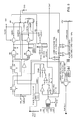
- FIG. 9 shows a full system block diagram of an exemplary power supply voltage regulator using active droop according to the present invention.
- the amount of droop is set by controlling the gain of an amplifier 202 that converts current to voltage, as shown.
- the current is sensed by measuring differentially the voltage across the regulator's MOSFET switch 204 while it is conducting.
- the amount measured is set by I DS times R DS (on) of the MOSFET, times the gain G of the differential amplifier 202 .
- the gain G of the amplifier 202 is set by a variable resistor 206 so that a different current level or different droop requirement can be incorporated by adjusting resistor 206 , without having to change MOSFET 204 .
- the output of amplifier 202 is used to set the amount of droop, for example, by controlling the regulator's reference voltage. This method can also be used to compensate for the positive temperature coefficient of R DS (on). By mounting resistor 206 in thermal contact with MOSFET switch 204 , and setting the gain from R to G to have a compensating negative temperature coefficient, the current sense can be made practically temperature independent; that is, as the temperature increases, the resistance of resistor 206 increases, which causes G to decrease.
- a single resistor in this invention thus permits droop to be set arbitrarily, independent of other operation at the power supply, without the efficiency penalty. It further permits temperature compensation at the current-sense element.
- the differential amplifier may be in an integrated circuit, so that the gain-setting resistor may be attached to a single pin of the IC.
- the gain could also be set by other means, such as a current source, etc.
- the current may be sensed in the low-side MOSFET switch, in which case the current would flow in a direction opposite to that shown in FIG. 2 .
- a resistor can be coupled to the source or drain of either the high-side MOSFET or low side MOSFET with the amplifier having inputs coupled across the resistor.
- FIG. 3 shows a simplified circuit diagram further illustrating the switching regulator and FET sensing scheme according to an embodiment of the present invention. More specifically, FIG. 3 shows a switching regulator 30 , which includes gain resistor 206 as was described in relation to FIG. 2 .
- FIG. 4 generally illustrates the FET sensing scheme according to an embodiment of the present invention.
- Comparator 302 compares the gate to source voltage (V gs ) on MOSFET switch 304 to a fixed reference voltage. When VGS is sufficiently greater than, V REF1 , the output of comparator 302 enables operational amplifier (opamp) 306 , by operation of switch 308 . Otherwise opamp 310 is enabled. When opamp 310 is enabled, the voltage at the output I SENSE equals the voltage, V SS .
- V(I SENSE ) is a function of V ds (on) and resistor 206 .
- V(I SENSE ) R( 312 ) ⁇ V ds (on)/R( 206 ) or R( 312 ) ⁇ I ds ⁇ R ds (ON)/R( 206 ).
- FIG. 5 shows in greater detail circuitry for implementing the embodiment shown in FIG. 4 .
- FIGS. 6 and 7 illustrate an alternate embodiment of the circuit implementation shown in FIGS. 4 and 5.
- the window detect circuit 600 monitors the gate of MOSFET switch 304 and the voltage to its driver, labeled “VCCH.” When the voltage at the gate of MOSFET switch 304 is within two diodes of VCCH, opamp 606 becomes active.
- the overall operation is substantially the same as in the embodiment shown in FIGS. 4 and 5 but this time shown in synchronous step down configuration.
- V ⁇ ( I SENSE ) R ⁇ ( 612 ) * IlxRds ⁇ ( ON ) R ⁇ ( 206 ) + V SS ⁇ ⁇ when ⁇ ⁇ 606 ⁇ ⁇ is ⁇ ⁇ active
- V V SS when 610 is active.
- the signal V SS is, for example, at about 2.5V and is used to bring Isense into the common mode range of the opamps and comparators.
- FIGS. 4-7 are driven by an asynchronous pulse width modulated (PWM) voltage controller in step down mode.
- PWM pulse width modulated
- FIG. 8 A simplified and exemplary PWM control loop according to another embodiment of the present invention is shown in FIG. 8 .
- the signal V(I SENSE ) (See FIGS. 4-7) is fed into a unity gain buffer 800 , followed by an amplifier 802 having, for example, a gain of two.
- a voltage error amplifier 804 having a fixed gain of, for example, 12 provides an amplified version of the difference in input voltages V REF and V FB .
- An opamp 806 sums the voltages, (V REF ⁇ V FB ), and V(I SENSE ).
- Comparator 810 operates as a maximum current limit comparator and takes into account the fact that R DS (on) can vary from one MOSFET to another by greater than 20%.
- resistor 206 in FIGS. 4-7 gives the PWM designer active control of load regulation.
- This control or active droop is used to reduce Vout under heavy load and keep the control transient response within a narrow window, e.g., +50 mV to ⁇ 70 mV of the initial target.
- An exemplary embodiment for a full system lock diagram is shown on the next page in FIG. 9 .
- the FET sensing circuitry including the window detect circuitry can be designed using various circuit components and implementations of the same.
- the inputs of an amplifier can be coupled to the drain and source of the low-side switch so that current sensing is accomplished via the current through the low-side switch.
- current sensing can be accomplished by inserting a resistor in series with the drain or source of either the high-side MOSFET or low-side MOSFET with the inputs of an amplifier (as, for example, in FIG. 2) coupled across the resistor's terminals. Accordingly, the true scope and spirit of the invention is instead indicated by the following claims and their equivalents.
Landscapes
- Engineering & Computer Science (AREA)
- Power Engineering (AREA)
- Dc-Dc Converters (AREA)
Abstract
Description

Claims (20)
Priority Applications (1)
| Application Number | Priority Date | Filing Date | Title |
|---|---|---|---|
| US09/656,499 US6528976B1 (en) | 1999-09-24 | 2000-09-07 | Fet sensing programmable active droop for power supplies |
Applications Claiming Priority (2)
| Application Number | Priority Date | Filing Date | Title |
|---|---|---|---|
| US15593499P | 1999-09-24 | 1999-09-24 | |
| US09/656,499 US6528976B1 (en) | 1999-09-24 | 2000-09-07 | Fet sensing programmable active droop for power supplies |
Publications (1)
| Publication Number | Publication Date |
|---|---|
| US6528976B1 true US6528976B1 (en) | 2003-03-04 |
Family
ID=26852721
Family Applications (1)
| Application Number | Title | Priority Date | Filing Date |
|---|---|---|---|
| US09/656,499 Expired - Lifetime US6528976B1 (en) | 1999-09-24 | 2000-09-07 | Fet sensing programmable active droop for power supplies |
Country Status (1)
| Country | Link |
|---|---|
| US (1) | US6528976B1 (en) |
Cited By (21)
| Publication number | Priority date | Publication date | Assignee | Title |
|---|---|---|---|---|
| US20030111984A1 (en) * | 2001-12-14 | 2003-06-19 | Intersil Americas Inc. | Programmable current-sensing circuit providing continuous temperature compensation for DC-DC converter |
| US20050024035A1 (en) * | 2003-06-30 | 2005-02-03 | Fereydun Tabaian | Programmable calibration circuit for power supply current sensing and droop loss compensation |
| US20050140348A1 (en) * | 2003-12-30 | 2005-06-30 | Delta Electronics, Inc. | Current distribution circuit |
| US20050275393A1 (en) * | 2004-06-14 | 2005-12-15 | Dialog Semiconductor Gmbh | Analog current sense circuit |
| US20060279350A1 (en) * | 2005-05-11 | 2006-12-14 | Xin Zhang | System and method for power management with scalable channel voltage regulation |
| US20070085589A1 (en) * | 2005-09-29 | 2007-04-19 | Kabushiki Kaisha Toshiba | Semiconductor device |
| US7425819B2 (en) | 2005-06-16 | 2008-09-16 | Microsemi Corporation | Slope compensation circuit |
| US7443698B2 (en) | 2004-11-22 | 2008-10-28 | Abb Research Ltd | Converter circuit for switching of a multiplicity of switching voltage levels |
| US20090058498A1 (en) * | 2007-08-29 | 2009-03-05 | Cambridge Semiconductor Limited | Half bridge circuit and method of operating a half bridge circuit |
| US20090134856A1 (en) * | 2007-11-26 | 2009-05-28 | Texas Instruments Incorporated | Method of optimum current blanking time implementation in current sense circuit |
| US20090153119A1 (en) * | 2007-12-17 | 2009-06-18 | Stmicroelectronics Sa | Method and device for measuring current for a dc-dc converter |
| FR2925167A1 (en) * | 2007-12-17 | 2009-06-19 | St Microelectronics Sa | CURRENT MEASURING DEVICE |
| US20090243712A1 (en) * | 2008-04-01 | 2009-10-01 | Richtek Technology Corporation | Device for reducing power consumption inside integrated circuit |
| US20100047617A1 (en) * | 2006-11-07 | 2010-02-25 | Natsuko Sugiura | High young's modulus steel plate and method of production of same |
| US7919952B1 (en) | 2005-03-21 | 2011-04-05 | Microsemi Corporation | Automatic gain control technique for current monitoring in current-mode switching regulators |
| US20150097539A1 (en) * | 2011-12-15 | 2015-04-09 | Texas Instruments Incorporated | Systems and methods for real-time inductor current simulation for a switching converter |
| US20150162834A1 (en) * | 2013-12-05 | 2015-06-11 | Fairchild Semiconductor Corporation | Dual-Mode Voltage Doubling Buck Converter With Smooth Mode Transition |
| US10008854B2 (en) | 2015-02-19 | 2018-06-26 | Enphase Energy, Inc. | Method and apparatus for time-domain droop control with integrated phasor current control |
| CN111953319A (en) * | 2019-05-17 | 2020-11-17 | 三星电机株式会社 | Amplification device with duty cycle based bias timing control circuit |
| CN117806407A (en) * | 2023-12-25 | 2024-04-02 | 普冉半导体(上海)股份有限公司 | A two-stage operational amplifier voltage regulating circuit and electronic equipment |
| US20250132673A1 (en) * | 2023-10-18 | 2025-04-24 | Stmicroelectronics International N.V. | Switching converter with valley current detection |
Citations (3)
| Publication number | Priority date | Publication date | Assignee | Title |
|---|---|---|---|---|
| US5081374A (en) * | 1990-02-22 | 1992-01-14 | National Semiconductor Corporation | Output buffer circuit with signal feed forward for reducing switching induced noise |
| US5982160A (en) * | 1998-12-24 | 1999-11-09 | Harris Corporation | DC-to-DC converter with inductor current sensing and related methods |
| US6057607A (en) * | 1999-07-16 | 2000-05-02 | Semtech Corporation | Method and apparatus for voltage regulation in multi-output switched mode power supplies |
-
2000
- 2000-09-07 US US09/656,499 patent/US6528976B1/en not_active Expired - Lifetime
Patent Citations (3)
| Publication number | Priority date | Publication date | Assignee | Title |
|---|---|---|---|---|
| US5081374A (en) * | 1990-02-22 | 1992-01-14 | National Semiconductor Corporation | Output buffer circuit with signal feed forward for reducing switching induced noise |
| US5982160A (en) * | 1998-12-24 | 1999-11-09 | Harris Corporation | DC-to-DC converter with inductor current sensing and related methods |
| US6057607A (en) * | 1999-07-16 | 2000-05-02 | Semtech Corporation | Method and apparatus for voltage regulation in multi-output switched mode power supplies |
Cited By (45)
| Publication number | Priority date | Publication date | Assignee | Title |
|---|---|---|---|---|
| US20030111984A1 (en) * | 2001-12-14 | 2003-06-19 | Intersil Americas Inc. | Programmable current-sensing circuit providing continuous temperature compensation for DC-DC converter |
| US6765372B2 (en) * | 2001-12-14 | 2004-07-20 | Intersil Americas Inc. | Programmable current-sensing circuit providing continuous temperature compensation for DC-DC Converter |
| USRE40915E1 (en) | 2001-12-14 | 2009-09-15 | Intersil Americas Inc. | Programmable current-sensing circuit providing continuous temperature compensation for DC-DC converter |
| USRE42037E1 (en) | 2001-12-14 | 2011-01-18 | Intersil Americas Inc. | Programmable current-sensing circuit providing continuous temperature compensation for DC-DC converter |
| US20050024035A1 (en) * | 2003-06-30 | 2005-02-03 | Fereydun Tabaian | Programmable calibration circuit for power supply current sensing and droop loss compensation |
| US20080231342A1 (en) * | 2003-06-30 | 2008-09-25 | Nupower Semiconductor, Inc. | Programmable calibration circuit for power supply current sensing and droop loss compensation |
| US7027944B2 (en) * | 2003-06-30 | 2006-04-11 | Nupower Semiconductor, Inc. | Programmable calibration circuit for power supply current sensing and droop loss compensation |
| US20060149486A1 (en) * | 2003-06-30 | 2006-07-06 | Nupower Semiconductor, Inc. | Programmable calibration circuit for power supply current sensing and droop loss compensation |
| US7383145B2 (en) | 2003-06-30 | 2008-06-03 | Nupower Semiconductor, Inc. | Programmable calibration circuit for power supply current sensing and droop loss compensation |
| US7580805B2 (en) * | 2003-06-30 | 2009-08-25 | Nupower Semiconductor, Inc. | Programmable calibration circuit for power supply current sensing and droop loss compensation |
| US20050140348A1 (en) * | 2003-12-30 | 2005-06-30 | Delta Electronics, Inc. | Current distribution circuit |
| US7170765B2 (en) * | 2003-12-30 | 2007-01-30 | Delta Electronics, Inc. | Current distribution circuit |
| US20050275393A1 (en) * | 2004-06-14 | 2005-12-15 | Dialog Semiconductor Gmbh | Analog current sense circuit |
| US7176665B2 (en) * | 2004-06-14 | 2007-02-13 | Dialog Semiconductor Gmbh | Analog current sense circuit |
| US7443698B2 (en) | 2004-11-22 | 2008-10-28 | Abb Research Ltd | Converter circuit for switching of a multiplicity of switching voltage levels |
| US7919952B1 (en) | 2005-03-21 | 2011-04-05 | Microsemi Corporation | Automatic gain control technique for current monitoring in current-mode switching regulators |
| US20060279350A1 (en) * | 2005-05-11 | 2006-12-14 | Xin Zhang | System and method for power management with scalable channel voltage regulation |
| WO2006122235A3 (en) * | 2005-05-11 | 2007-11-29 | Virginia Tech Intell Prop | System and method for power management with scalable channel voltage regulation |
| US7425819B2 (en) | 2005-06-16 | 2008-09-16 | Microsemi Corporation | Slope compensation circuit |
| US7492133B2 (en) | 2005-09-29 | 2009-02-17 | Kabushiki Kaisha Toshiba | Semiconductor device configured to complementarily control on/off of a high-side switching element |
| US20080024093A1 (en) * | 2005-09-29 | 2008-01-31 | Kabushiki Kaisha Toshiba | Semiconductor device |
| US7294992B2 (en) * | 2005-09-29 | 2007-11-13 | Kabushiki Kaisha Toshiba | Semiconductor device, with an off detection circuit |
| US20070085589A1 (en) * | 2005-09-29 | 2007-04-19 | Kabushiki Kaisha Toshiba | Semiconductor device |
| US20100047617A1 (en) * | 2006-11-07 | 2010-02-25 | Natsuko Sugiura | High young's modulus steel plate and method of production of same |
| US20090058498A1 (en) * | 2007-08-29 | 2009-03-05 | Cambridge Semiconductor Limited | Half bridge circuit and method of operating a half bridge circuit |
| US7531993B2 (en) * | 2007-08-29 | 2009-05-12 | Cambridge Semiconductor Limited | Half bridge circuit and method of operating a half bridge circuit |
| US20090134856A1 (en) * | 2007-11-26 | 2009-05-28 | Texas Instruments Incorporated | Method of optimum current blanking time implementation in current sense circuit |
| US7868599B2 (en) * | 2007-11-26 | 2011-01-11 | Texas Instruments Incorporated | Method of optimum current blanking time implementation in current sense circuit |
| US20090153119A1 (en) * | 2007-12-17 | 2009-06-18 | Stmicroelectronics Sa | Method and device for measuring current for a dc-dc converter |
| US20090167261A1 (en) * | 2007-12-17 | 2009-07-02 | Stmicroelectronics Sa | Current measuring device |
| FR2925167A1 (en) * | 2007-12-17 | 2009-06-19 | St Microelectronics Sa | CURRENT MEASURING DEVICE |
| US8692534B2 (en) | 2007-12-17 | 2014-04-08 | St-Ericsson Sa | Current measuring device |
| US20090243712A1 (en) * | 2008-04-01 | 2009-10-01 | Richtek Technology Corporation | Device for reducing power consumption inside integrated circuit |
| US10630183B2 (en) | 2011-12-15 | 2020-04-21 | Texas Instruments Incorporated | Systems and methods for real-time inductor current simulation for a switching converter |
| US20150097539A1 (en) * | 2011-12-15 | 2015-04-09 | Texas Instruments Incorporated | Systems and methods for real-time inductor current simulation for a switching converter |
| US9966855B2 (en) * | 2011-12-15 | 2018-05-08 | Texas Instruments Incorporated | Systems and methods for real-time inductor current simulation for a switching converter |
| US20150162834A1 (en) * | 2013-12-05 | 2015-06-11 | Fairchild Semiconductor Corporation | Dual-Mode Voltage Doubling Buck Converter With Smooth Mode Transition |
| US9647546B2 (en) * | 2013-12-05 | 2017-05-09 | Fairchild Semiconductor Corporation | Dual-mode voltage doubling buck converter with smooth mode transition |
| US10008854B2 (en) | 2015-02-19 | 2018-06-26 | Enphase Energy, Inc. | Method and apparatus for time-domain droop control with integrated phasor current control |
| US10951037B2 (en) | 2015-02-19 | 2021-03-16 | Enphase Energy, Inc. | Method and apparatus for time-domain droop control with integrated phasor current control |
| US11355936B2 (en) | 2015-02-19 | 2022-06-07 | Enphase Energy, Inc. | Method and apparatus for time-domain droop control with integrated phasor current control |
| CN111953319A (en) * | 2019-05-17 | 2020-11-17 | 三星电机株式会社 | Amplification device with duty cycle based bias timing control circuit |
| US20250132673A1 (en) * | 2023-10-18 | 2025-04-24 | Stmicroelectronics International N.V. | Switching converter with valley current detection |
| US12609617B2 (en) * | 2023-10-18 | 2026-04-21 | Stmicroelectronics International N.V. | Switching converter with valley current detection |
| CN117806407A (en) * | 2023-12-25 | 2024-04-02 | 普冉半导体(上海)股份有限公司 | A two-stage operational amplifier voltage regulating circuit and electronic equipment |
Similar Documents
| Publication | Publication Date | Title |
|---|---|---|
| US6528976B1 (en) | Fet sensing programmable active droop for power supplies | |
| US6366068B1 (en) | Switching power supply with overcurrent protection and method | |
| US7034586B2 (en) | Startup circuit for converter with pre-biased load | |
| US6850044B2 (en) | Hybrid regulator with switching and linear sections | |
| USRE40915E1 (en) | Programmable current-sensing circuit providing continuous temperature compensation for DC-DC converter | |
| US6642696B2 (en) | DC-DC converter with a feedback controller | |
| US7859511B2 (en) | DC-DC converter with temperature compensation circuit | |
| US6894466B2 (en) | Active current sharing circuit | |
| US6160388A (en) | Sensing of current in a synchronous-buck power stage | |
| KR100744592B1 (en) | Dc-dc converter, dc-dc converter control circuit, and dc-dc converter control method | |
| EP0529391A1 (en) | Voltage converter | |
| KR20110118076A (en) | Detection and Compensation System and Method of Aggressive Output Filter for Switch Mode Power Supplies | |
| CN100511077C (en) | Capacitance feedback circuit | |
| US7750617B2 (en) | Switching regulator and electronic device therewith | |
| US7151361B2 (en) | Current sensing circuitry for DC-DC converters | |
| EP2908417A1 (en) | High speed regulator with low capacitor values | |
| US8692534B2 (en) | Current measuring device | |
| JP2004343997A (en) | Active voltage positioning method and implementation | |
| US7023191B2 (en) | Voltage regulator with adjustable output impedance | |
| KR101058935B1 (en) | Switching-mode power supplies | |
| US7859242B2 (en) | DC-DC Converter | |
| US20100194362A1 (en) | Regulator with pulse width modulation circuit | |
| TWI868536B (en) | Feedback circuit of a voltage regulator and a feedback control method applicable to a voltage regulator | |
| TWI381511B (en) | Single pin multi-function singal detection method and structure therefor | |
| CN212278125U (en) | Power supply control device and switching power supply system |
Legal Events
| Date | Code | Title | Description |
|---|---|---|---|
| AS | Assignment |
Owner name: FAERCHILD SEMICONDUCTOR CORPORATION, MAINE Free format text: ASSIGNMENT OF ASSIGNORS INTEREST;ASSIGNORS:LENK, RONALD J.;ROSSETTI, NAZZARENO;SMITH, KIMBLE;AND OTHERS;REEL/FRAME:011381/0925;SIGNING DATES FROM 20001121 TO 20001123 |
|
| STCF | Information on status: patent grant |
Free format text: PATENTED CASE |
|
| FPAY | Fee payment |
Year of fee payment: 4 |
|
| FPAY | Fee payment |
Year of fee payment: 8 |
|
| FPAY | Fee payment |
Year of fee payment: 12 |
|
| AS | Assignment |
Owner name: FAIRCHILD SEMICONDUCTOR CORPORATION, MAINE Free format text: CORRECTIVE ASSIGNMENT TO CORRECT THE NAME OF THE RECEIVING PARTY PREVIOUSLY RECORDED ON REEL 011381 FRAME 0925. ASSIGNOR(S) HEREBY CONFIRMS THE ASSIGNMENT;ASSIGNORS:LENK, RONALD J;ROSSETTI, NAZZARENO;SMITH, KIMBLE;AND OTHERS;SIGNING DATES FROM 20001121 TO 20001123;REEL/FRAME:039429/0351 |
|
| AS | Assignment |
Owner name: DEUTSCHE BANK AG NEW YORK BRANCH, AS COLLATERAL AGENT, NEW YORK Free format text: PATENT SECURITY AGREEMENT;ASSIGNOR:FAIRCHILD SEMICONDUCTOR CORPORATION;REEL/FRAME:040075/0644 Effective date: 20160916 Owner name: DEUTSCHE BANK AG NEW YORK BRANCH, AS COLLATERAL AG Free format text: PATENT SECURITY AGREEMENT;ASSIGNOR:FAIRCHILD SEMICONDUCTOR CORPORATION;REEL/FRAME:040075/0644 Effective date: 20160916 |
|
| AS | Assignment |
Owner name: SEMICONDUCTOR COMPONENTS INDUSTRIES, LLC, ARIZONA Free format text: ASSIGNMENT OF ASSIGNORS INTEREST;ASSIGNOR:FAIRCHILD SEMICONDUCTOR CORPORATION;REEL/FRAME:057694/0374 Effective date: 20210722 |
|
| AS | Assignment |
Owner name: FAIRCHILD SEMICONDUCTOR CORPORATION, ARIZONA Free format text: RELEASE BY SECURED PARTY;ASSIGNOR:DEUTSCHE BANK AG NEW YORK BRANCH;REEL/FRAME:057969/0206 Effective date: 20211027 Owner name: FAIRCHILD SEMICONDUCTOR CORPORATION, ARIZONA Free format text: RELEASE OF SECURITY INTEREST;ASSIGNOR:DEUTSCHE BANK AG NEW YORK BRANCH;REEL/FRAME:057969/0206 Effective date: 20211027 |
|
| AS | Assignment |
Owner name: DEUTSCHE BANK AG NEW YORK BRANCH, AS COLLATERAL AGENT, NEW YORK Free format text: SECURITY INTEREST;ASSIGNOR:SEMICONDUCTOR COMPONENTS INDUSTRIES, LLC;REEL/FRAME:058871/0799 Effective date: 20211028 |
|
| AS | Assignment |
Owner name: FAIRCHILD SEMICONDUCTOR CORPORATION, ARIZONA Free format text: RELEASE OF SECURITY INTEREST IN PATENTS RECORDED AT REEL 040075, FRAME 0644;ASSIGNOR:DEUTSCHE BANK AG NEW YORK BRANCH, AS COLLATERAL AGENT;REEL/FRAME:064070/0536 Effective date: 20230622 Owner name: SEMICONDUCTOR COMPONENTS INDUSTRIES, LLC, ARIZONA Free format text: RELEASE OF SECURITY INTEREST IN PATENTS RECORDED AT REEL 040075, FRAME 0644;ASSIGNOR:DEUTSCHE BANK AG NEW YORK BRANCH, AS COLLATERAL AGENT;REEL/FRAME:064070/0536 Effective date: 20230622 |
|
| AS | Assignment |
Owner name: FAIRCHILD SEMICONDUCTOR CORPORATION, ARIZONA Free format text: RELEASE OF SECURITY INTEREST IN PATENTS RECORDED AT REEL 058871, FRAME 0799;ASSIGNOR:DEUTSCHE BANK AG NEW YORK BRANCH, AS COLLATERAL AGENT;REEL/FRAME:065653/0001 Effective date: 20230622 Owner name: SEMICONDUCTOR COMPONENTS INDUSTRIES, LLC, ARIZONA Free format text: RELEASE OF SECURITY INTEREST IN PATENTS RECORDED AT REEL 058871, FRAME 0799;ASSIGNOR:DEUTSCHE BANK AG NEW YORK BRANCH, AS COLLATERAL AGENT;REEL/FRAME:065653/0001 Effective date: 20230622 |