US6445043B1 - Isolated regions in an integrated circuit - Google Patents
Isolated regions in an integrated circuit Download PDFInfo
- Publication number
- US6445043B1 US6445043B1 US08/347,527 US34752794A US6445043B1 US 6445043 B1 US6445043 B1 US 6445043B1 US 34752794 A US34752794 A US 34752794A US 6445043 B1 US6445043 B1 US 6445043B1
- Authority
- US
- United States
- Prior art keywords
- dopant
- silicon
- substrate
- active device
- top surface
- Prior art date
- Legal status (The legal status is an assumption and is not a legal conclusion. Google has not performed a legal analysis and makes no representation as to the accuracy of the status listed.)
- Expired - Lifetime
Links
Images

Classifications
-
- H10W10/014—
-
- H10W10/17—
Definitions
- This invention relates to semiconductor integrated circuits and more particularly to methods for producing electrically isolated devices in such circuits.
- MOS metal oxide semiconductor
- bipolar transistors Various techniques have been utilized in integrated circuit manufacturing processes to form isolated regions on silicon wafers in which various microelectronic devices, e.g., metal oxide semiconductor (MOS) and bipolar transistors, can be formed.
- MOS metal oxide semiconductor
- the primary advantages gained by providing isolated regions on silicon wafers are the reduced parasitic capacitive coupling of devices to the wafers and the excellent inter-isolation of devices formed in different regions on the wafers.
- a commonly used method for manufacturing MOS transistors and bipolar transistors in integrated circuits at a major surface of a semiconductive silicon substrate involves the local oxidation of silicon (LOCOS) process for electrically isolating neighboring transistors.
- LOCOS local oxidation of silicon
- a major surface of a silicon substrate is masked with a silicon dioxide or silicon nitride layer having window areas and the exposed silicon in these window areas is oxidized.
- the LOCOS process undesirably increases the required distance between neighboring transistors and undesirably reduces transistor packing density.
- SEG selective epitaxial growth
- MOS and bipolar circuits are commonly fabricated on a single epitaxial silicon layer which has been uniformly doped to a single, fixed dopant concentration.
- the number of variables which can be controlled during manufacture of both MOS and bipolar devices on a single epitaxial silicon layer is limited by the fixed concentration of dopant in the epitaxial silicon.
- a process for forming isolated active device regions on a silicon substrate involves forming at least one trench in a silicon substrate to define at least two active device regions on the substrate to be electrically isolated from each other, filling the trench with an electrically insulative material, performing a masking and etching operation to expose at least one active device region on the substrate, selectively growing a first epitaxial layer of silicon on the exposed active device region, performing a masking and etching operation to expose at least one other active device region on the substrate and selectively growing a second epitaxial layer of silicon on the other exposed active device region on the substrate, the first epitaxial layer and second epitaxial layer being doped with impurity ions to the same or different doping concentrations to provide at least two isolated active device regions on the silicon substrate.
- CMOS and bipolar devices can be formed simultaneously and independently of each other on the same chip.
- the process of the invention is carried out with a minimum of operations and avoids the need to make costly modifications to manufacturing operations.
- performance optimized as utilized herein shall be understood to refer to devices which are maximized for current and/or voltage gain.
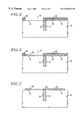
- FIGS. 1-7 are diagrammatic cross-sectional views showing successive stages of processing of a silicon substrate having two isolated active device regions.
- FIGS. 1-7 illustrate, for purposes of example only, a process in which electrical isolation between active device regions on a silicon substrate is obtained. It should be understood, however, that each of the principles and concepts of the invention, as described in detail below, can be modified in various ways without deviating from the scope and spirit of this invention.
- Trench 12 defines active device region 14 and active device region 16 on silicon substrate 10 .
- Silicon substrate 10 is a silicon wafer formed by the well-known Czochralski technique and can possess any desired orientation such as a (100), (110), or (111) orientation as is familiar to those skilled in the art.
- Trench 12 is typically etched into substrate 10 to a depth which ranges from about 0.25 to about 5 ⁇ m and a width which ranges from about 0.25 to about 5 ⁇ m.
- Trench 12 can be formed utilizing any suitable technique, e.g., reactive plasma etching, which is known to be suitable for this purpose.
- Silicon substrate 10 can also be heavily or lightly doped with an impurity such as boron, phosphorus or antimony.
- the impurity can be diffused into substrate 10 by heating the substrate to a drive-in temperature ranging from about 700 to about 1200° C. for a drive-in time varying from 1 to about 6 hours.
- a drive-in temperature ranging from about 700 to about 1200° C. for a drive-in time varying from 1 to about 6 hours.
- Persons skilled in the art will be familiar with the temperatures and times suited to different dopants and different depths within substrate 10 .
- an electrically insulative material 18 e.g., silicon dioxide, silicon nitride, tetraethoxysilane, or combination thereof, is deposited on substrate 10 to fill trench 12 .
- silicon dioxide is deposited in trench 12 by conventional chemical vapor deposition techniques such as those described in Chapter 6 of S. M. Sze, VLSI Technology, Second Edition, McGraw-Hill Book Company (1988).
- the surface of substrate 10 is planarized by known chemical and/or mechanical methods to provide a substantially uniform planar surface as illustrated in FIG. 2 .
- masking layer 20 composed of an oxide (SiO 2 ) or nitride (Si 3 N 4 ) or other suitable material is formed on the surface of substrate 10 and thereafter selectively etched utilizing techniques which are well known in the art to provide window 22 exposing active device region 16 on substrate 10 .
- layer 20 masks active device region 14 and trench 12 .
- Exposed active device region 16 can optionally be etched to remove any residual surface damage that may have occurred during the opening of window 22 . Such an etch is preferably performed by subjecting the wafer to a dilute mixture of HF and H 2 O and HNO 3 .
- first epitaxial layer 30 of silicon is then selectively grown on exposed active device region 16 by means of conventional epitaxial deposition techniques such as vapor-phase epitaxy, i.e., chemical vapor deposition, or molecular beam epitaxy. Thickness of first epitaxial layer 30 of silicon can broadly range from about 0.5 to about 50 microns. Preferably, the growth process employed is a Type I growth process in which epitaxial silicon is grown only on exposed regions of substrate 10 and not on masking layer 20 . First epitaxial layer 30 of silicon can be doped with an impurity while being grown on substrate 10 and/or be doped via ion implantation and annealing after first epitaxial layer 30 has been grown.
- conventional epitaxial deposition techniques such as vapor-phase epitaxy, i.e., chemical vapor deposition, or molecular beam epitaxy.
- Thickness of first epitaxial layer 30 of silicon can broadly range from about 0.5 to about 50 microns.
- the growth process employed is a Type
- First epitaxial layer 30 of silicon can be doped with an impurity such as boron, phosphorus, arsenic, and the like, at a dopant concentration which ranges from about 1 ⁇ 10 11 to about 1 ⁇ 10 17 ions/cm 2 , preferably from about 1 ⁇ 10 12 to about 1 ⁇ 10 13 ions/cm 2 .
- Various devices can later be formed at first epitaxial layer 30 .
- a performance-optimized MOS-type device can be formed at first epitaxial layer in accordance with known procedures.
- oxide or nitride layer 20 is stripped by, e.g., wet or dry etch, and, as shown in FIG. 5, oxide or nitride masking layer 40 is formed on the surface of substrate 10 .
- Masking layer 40 is selectively etched in accordance with well known techniques to mask trench 12 and first epitaxial layer 30 and provide window 42 which exposes active device region 14 on substrate 10 .
- Exposed active device region 14 can optionally be etched to remove any residual surface damage that may have occurred during the opening of window 42 .
- Such an etch is preferably performed by subjecting the wafer to a dilute mixture of HF and H 2 O and HNO 3 .
- second epitaxial layer 50 of silicon is selectively grown on active device region 14 by means of a conventional epitaxial growth technique such as vapor-phase epitaxy and molecular beam epitaxy. Likewise, a Type I growth process is preferably employed. Thickness of second epitaxial layer 50 of silicon can broadly range from about 0.5 to about 50 microns. Second epitaxial layer 50 can be doped with an impurity while being grown on substrate 10 and/or be doped via ion implantation and annealing after being grown.
- Impurities such as boron, phosphorus, arsenic, and the like, can be diffused or implanted in second epitaxial layer 50 at a dopant concentration which ranges from about 1 ⁇ 10 11 to about 1 ⁇ 10 17 ions/cm 2 , preferably from about 1 ⁇ 10 12 to about 1 ⁇ 10 13 ions/cm 3 .
- the dopant concentration of the second epitaxial layer of silicon can be the same or different as the dopant concentration of the first epitaxial layer of silicon.
- a performance-optimized bipolar device can later be formed at second epitaxial layer 50 in accordance with known procedures.
- oxide or nitride masking layer 40 is removed by, e.g., wet or dry etch.
- an electrically insulative material 60 such as silicon dioxide, silicon nitride, tetraethoxysilane, or the like, can be deposited on substrate 10 and thereafter planarized to provide a substantially planar surface as shown in FIG. 7 .
- MOS and bipolar devices which are individually performance optimized can thereafter be simultaneously formed on epitaxial layers 30 and 50 .
- Performance-optimized devices that can simultaneously be formed on epitaxial layers 30 and 50 in accordance with this invention include MOS devices, e.g., n-MOS, p-MOS and CMOS devices, bipolar devices, capacitors, resistors, thin-film transistors, heterojunction devices, to name just a few.
- MOS devices e.g., n-MOS, p-MOS and CMOS devices
- bipolar devices capacitors, resistors, thin-film transistors, heterojunction devices, to name just a few.
- a CMOS and bipolar device e.g., vertical bipolar transistor, are simultaneously and independently formed on epitaxial layers 30 and 50 .
- the current gains of these devices can be optimized based on the specific application of each device in accordance with this invention.
- an integrated circuit possessing at least two different devices which are independently performance optimized.
- first epitaxial layer and second epitaxial layer herein can be doped with different dopant atoms.
Landscapes
- Element Separation (AREA)
- Weting (AREA)
- Physical Deposition Of Substances That Are Components Of Semiconductor Devices (AREA)
- Metal-Oxide And Bipolar Metal-Oxide Semiconductor Integrated Circuits (AREA)
Abstract
Description
Claims (20)
Priority Applications (3)
| Application Number | Priority Date | Filing Date | Title |
|---|---|---|---|
| US08/347,527 US6445043B1 (en) | 1994-11-30 | 1994-11-30 | Isolated regions in an integrated circuit |
| JP31147395A JP3396571B2 (en) | 1994-11-30 | 1995-11-30 | Process for forming isolation region in integrated circuit and formed structure |
| US08/620,964 US5763314A (en) | 1994-11-30 | 1996-03-22 | Process for forming isolation regions in an integrated circuit |
Applications Claiming Priority (1)
| Application Number | Priority Date | Filing Date | Title |
|---|---|---|---|
| US08/347,527 US6445043B1 (en) | 1994-11-30 | 1994-11-30 | Isolated regions in an integrated circuit |
Related Child Applications (1)
| Application Number | Title | Priority Date | Filing Date |
|---|---|---|---|
| US08/620,964 Division US5763314A (en) | 1994-11-30 | 1996-03-22 | Process for forming isolation regions in an integrated circuit |
Publications (1)
| Publication Number | Publication Date |
|---|---|
| US6445043B1 true US6445043B1 (en) | 2002-09-03 |
Family
ID=23364086
Family Applications (2)
| Application Number | Title | Priority Date | Filing Date |
|---|---|---|---|
| US08/347,527 Expired - Lifetime US6445043B1 (en) | 1994-11-30 | 1994-11-30 | Isolated regions in an integrated circuit |
| US08/620,964 Expired - Lifetime US5763314A (en) | 1994-11-30 | 1996-03-22 | Process for forming isolation regions in an integrated circuit |
Family Applications After (1)
| Application Number | Title | Priority Date | Filing Date |
|---|---|---|---|
| US08/620,964 Expired - Lifetime US5763314A (en) | 1994-11-30 | 1996-03-22 | Process for forming isolation regions in an integrated circuit |
Country Status (2)
| Country | Link |
|---|---|
| US (2) | US6445043B1 (en) |
| JP (1) | JP3396571B2 (en) |
Cited By (2)
| Publication number | Priority date | Publication date | Assignee | Title |
|---|---|---|---|---|
| US20020014666A1 (en) * | 1999-11-30 | 2002-02-07 | Tadahiro Ohmi | Semiconductor device formed on (111) surface of a si crystal and fabrication process thereof |
| US20050136584A1 (en) * | 2003-12-23 | 2005-06-23 | Boyan Boyanov | Strained transistor integration for CMOS |
Families Citing this family (7)
| Publication number | Priority date | Publication date | Assignee | Title |
|---|---|---|---|---|
| US5748547A (en) * | 1996-05-24 | 1998-05-05 | Shau; Jeng-Jye | High performance semiconductor memory devices having multiple dimension bit lines |
| US6319772B1 (en) | 2000-10-30 | 2001-11-20 | Chartered Semiconductor Manufacturing Ltd. | Method for making low-leakage DRAM structures using selective silicon epitaxial growth (SEG) on an insulating layer |
| US7141478B2 (en) * | 2004-01-26 | 2006-11-28 | Legerity Inc. | Multi-stage EPI process for forming semiconductor devices, and resulting device |
| US20060105533A1 (en) * | 2004-11-16 | 2006-05-18 | Chong Yung F | Method for engineering hybrid orientation/material semiconductor substrate |
| US7547605B2 (en) * | 2004-11-22 | 2009-06-16 | Taiwan Semiconductor Manufacturing Company | Microelectronic device and a method for its manufacture |
| KR100683401B1 (en) * | 2005-08-11 | 2007-02-15 | 동부일렉트로닉스 주식회사 | Semiconductor Device Using Epilayer and Manufacturing Method Thereof |
| US10622262B2 (en) * | 2017-10-06 | 2020-04-14 | Newport Fab Llc | High performance SiGe heterojunction bipolar transistors built on thin film silicon-on-insulator substrates for radio frequency applications |
Citations (24)
| Publication number | Priority date | Publication date | Assignee | Title |
|---|---|---|---|---|
| US4619033A (en) * | 1985-05-10 | 1986-10-28 | Rca Corporation | Fabricating of a CMOS FET with reduced latchup susceptibility |
| JPS62132342A (en) * | 1985-12-05 | 1987-06-15 | Matsushita Electric Ind Co Ltd | Manufacturing method of semiconductor integrated circuit |
| US4808598A (en) * | 1986-06-30 | 1989-02-28 | The United States Of America As Represented By The Secretary Of The Army | Method for inducing protection in an animal against cyanide poisoning using 8-aminoquinolines |
| US4929570A (en) * | 1986-10-06 | 1990-05-29 | National Semiconductor Corporation | Selective epitaxy BiCMOS process |
| US4960726A (en) * | 1989-10-19 | 1990-10-02 | International Business Machines Corporation | BiCMOS process |
| US5015594A (en) * | 1988-10-24 | 1991-05-14 | International Business Machines Corporation | Process of making BiCMOS devices having closely spaced device regions |
| US5049513A (en) * | 1990-09-17 | 1991-09-17 | Texas Instruments Incorporated | Bi CMOS/SOI process flow |
| US5073516A (en) | 1991-02-28 | 1991-12-17 | Texas Instruments Incorporated | Selective epitaxial growth process flow for semiconductor technologies |
| US5079183A (en) * | 1983-07-15 | 1992-01-07 | Kabushiki Kaisha Toshiba | C-mos device and a process for manufacturing the same |
| US5097314A (en) * | 1988-02-08 | 1992-03-17 | Kabushiki Kaisha Toshiba | Dielectrically isolated substrate with isolated high and low breakdown voltage elements |
| US5132234A (en) | 1991-02-25 | 1992-07-21 | Samsung Electronics Co., Ltd. | Method of producing a bipolar CMOS device |
| US5156984A (en) | 1987-12-31 | 1992-10-20 | Goldstar Co., Ltd. | Manufacturing method for a bi-cmos by trenching |
| US5164326A (en) | 1992-03-30 | 1992-11-17 | Motorola, Inc. | Complementary bipolar and CMOS on SOI |
| US5179040A (en) * | 1990-07-16 | 1993-01-12 | Mitsubishi Denki Kabushiki Kaisha | Method of making a semiconductor laser device |
| US5206182A (en) | 1989-06-08 | 1993-04-27 | United Technologies Corporation | Trench isolation process |
| US5234845A (en) | 1991-04-12 | 1993-08-10 | Hitachi, Ltd. | Method of manufacturing semiconductor IC using selective poly and EPI silicon growth |
| US5298450A (en) | 1987-12-10 | 1994-03-29 | Texas Instruments Incorporated | Process for simultaneously fabricating isolation structures for bipolar and CMOS circuits |
| US5306939A (en) | 1990-04-05 | 1994-04-26 | Seh America | Epitaxial silicon wafers for CMOS integrated circuits |
| US5319235A (en) * | 1989-11-21 | 1994-06-07 | Kabushiki Kaisha Toshiba | Monolithic IC formed of a CCD, CMOS and a bipolar element |
| US5326710A (en) | 1992-09-10 | 1994-07-05 | National Semiconductor Corporation | Process for fabricating lateral PNP transistor structure and BICMOS IC |
| US5331225A (en) | 1990-07-25 | 1994-07-19 | Kabushiki Kaisha Toshiba | BiCMOS logic circuit with bipolar transistor and MOS transistor formed on the same semiconductor substrate |
| US5338699A (en) | 1990-05-02 | 1994-08-16 | Mitsubishi Denki Kabushiki Kaisha | Method of making a semiconductor integrated device having gate sidewall structure |
| US5436189A (en) * | 1989-10-03 | 1995-07-25 | Harris Corporation | Self-aligned channel stop for trench-isolated island |
| US5525824A (en) * | 1993-11-09 | 1996-06-11 | Nippondenso Co., Ltd. | Semiconductor device with isolation regions |
Family Cites Families (2)
| Publication number | Priority date | Publication date | Assignee | Title |
|---|---|---|---|---|
| JPS6021560A (en) * | 1983-07-15 | 1985-02-02 | Toshiba Corp | Complementary type mos semiconductor device and manufacture thereof |
| JPH01186669A (en) * | 1988-01-14 | 1989-07-26 | Nec Corp | Manufacture of semiconductor device |
-
1994
- 1994-11-30 US US08/347,527 patent/US6445043B1/en not_active Expired - Lifetime
-
1995
- 1995-11-30 JP JP31147395A patent/JP3396571B2/en not_active Expired - Lifetime
-
1996
- 1996-03-22 US US08/620,964 patent/US5763314A/en not_active Expired - Lifetime
Patent Citations (24)
| Publication number | Priority date | Publication date | Assignee | Title |
|---|---|---|---|---|
| US5079183A (en) * | 1983-07-15 | 1992-01-07 | Kabushiki Kaisha Toshiba | C-mos device and a process for manufacturing the same |
| US4619033A (en) * | 1985-05-10 | 1986-10-28 | Rca Corporation | Fabricating of a CMOS FET with reduced latchup susceptibility |
| JPS62132342A (en) * | 1985-12-05 | 1987-06-15 | Matsushita Electric Ind Co Ltd | Manufacturing method of semiconductor integrated circuit |
| US4808598A (en) * | 1986-06-30 | 1989-02-28 | The United States Of America As Represented By The Secretary Of The Army | Method for inducing protection in an animal against cyanide poisoning using 8-aminoquinolines |
| US4929570A (en) * | 1986-10-06 | 1990-05-29 | National Semiconductor Corporation | Selective epitaxy BiCMOS process |
| US5298450A (en) | 1987-12-10 | 1994-03-29 | Texas Instruments Incorporated | Process for simultaneously fabricating isolation structures for bipolar and CMOS circuits |
| US5156984A (en) | 1987-12-31 | 1992-10-20 | Goldstar Co., Ltd. | Manufacturing method for a bi-cmos by trenching |
| US5097314A (en) * | 1988-02-08 | 1992-03-17 | Kabushiki Kaisha Toshiba | Dielectrically isolated substrate with isolated high and low breakdown voltage elements |
| US5015594A (en) * | 1988-10-24 | 1991-05-14 | International Business Machines Corporation | Process of making BiCMOS devices having closely spaced device regions |
| US5206182A (en) | 1989-06-08 | 1993-04-27 | United Technologies Corporation | Trench isolation process |
| US5436189A (en) * | 1989-10-03 | 1995-07-25 | Harris Corporation | Self-aligned channel stop for trench-isolated island |
| US4960726A (en) * | 1989-10-19 | 1990-10-02 | International Business Machines Corporation | BiCMOS process |
| US5319235A (en) * | 1989-11-21 | 1994-06-07 | Kabushiki Kaisha Toshiba | Monolithic IC formed of a CCD, CMOS and a bipolar element |
| US5306939A (en) | 1990-04-05 | 1994-04-26 | Seh America | Epitaxial silicon wafers for CMOS integrated circuits |
| US5338699A (en) | 1990-05-02 | 1994-08-16 | Mitsubishi Denki Kabushiki Kaisha | Method of making a semiconductor integrated device having gate sidewall structure |
| US5179040A (en) * | 1990-07-16 | 1993-01-12 | Mitsubishi Denki Kabushiki Kaisha | Method of making a semiconductor laser device |
| US5331225A (en) | 1990-07-25 | 1994-07-19 | Kabushiki Kaisha Toshiba | BiCMOS logic circuit with bipolar transistor and MOS transistor formed on the same semiconductor substrate |
| US5049513A (en) * | 1990-09-17 | 1991-09-17 | Texas Instruments Incorporated | Bi CMOS/SOI process flow |
| US5132234A (en) | 1991-02-25 | 1992-07-21 | Samsung Electronics Co., Ltd. | Method of producing a bipolar CMOS device |
| US5073516A (en) | 1991-02-28 | 1991-12-17 | Texas Instruments Incorporated | Selective epitaxial growth process flow for semiconductor technologies |
| US5234845A (en) | 1991-04-12 | 1993-08-10 | Hitachi, Ltd. | Method of manufacturing semiconductor IC using selective poly and EPI silicon growth |
| US5164326A (en) | 1992-03-30 | 1992-11-17 | Motorola, Inc. | Complementary bipolar and CMOS on SOI |
| US5326710A (en) | 1992-09-10 | 1994-07-05 | National Semiconductor Corporation | Process for fabricating lateral PNP transistor structure and BICMOS IC |
| US5525824A (en) * | 1993-11-09 | 1996-06-11 | Nippondenso Co., Ltd. | Semiconductor device with isolation regions |
Non-Patent Citations (1)
| Title |
|---|
| Wolf, S., "Silicon Processing for the VLSI Era: vol. 2, Process Integration", Lattice Press, 1990, p 558. * |
Cited By (13)
| Publication number | Priority date | Publication date | Assignee | Title |
|---|---|---|---|---|
| US7795106B2 (en) | 1999-11-30 | 2010-09-14 | Tadahiro Ohmi | Semiconductor device formed on (111) surface of a Si crystal and fabrication process thereof |
| US20050087831A1 (en) * | 1999-11-30 | 2005-04-28 | Tadahiro Ohmi | Semiconductor device formed on (111) surface of a Si crystal and fabrication process thereof |
| US7012311B2 (en) * | 1999-11-30 | 2006-03-14 | Tadahiro Ohmi | Semiconductor device formed on (111) surface of a Si crystal and fabrication process thereof |
| US20080128758A1 (en) * | 1999-11-30 | 2008-06-05 | Tadahiro Ohmi | Semiconductor device formed on (111) surface of a Si crystal and fabrication process thereof |
| US20080224145A1 (en) * | 1999-11-30 | 2008-09-18 | Tadahiro Ohmi | Semiconductor device formed on (111) surface of a Si crystal and fabrication process thereof |
| US7759762B2 (en) | 1999-11-30 | 2010-07-20 | Tadahiro Ohmi | Semiconductor device formed on (111) surface of a Si crystal and fabrication process thereof |
| US20020014666A1 (en) * | 1999-11-30 | 2002-02-07 | Tadahiro Ohmi | Semiconductor device formed on (111) surface of a si crystal and fabrication process thereof |
| US20050136584A1 (en) * | 2003-12-23 | 2005-06-23 | Boyan Boyanov | Strained transistor integration for CMOS |
| US7662689B2 (en) * | 2003-12-23 | 2010-02-16 | Intel Corporation | Strained transistor integration for CMOS |
| US20100044754A1 (en) * | 2003-12-23 | 2010-02-25 | Boyan Boyanov | Strained transistor integration for cmos |
| US8373154B2 (en) | 2003-12-23 | 2013-02-12 | Intel Corporation | Strained transistor integration for CMOS |
| US8748869B2 (en) | 2003-12-23 | 2014-06-10 | Intel Corporation | Strained transistor integration for CMOS |
| US9112029B2 (en) | 2003-12-23 | 2015-08-18 | Intel Corporation | Strained transistor integration for CMOS |
Also Published As
| Publication number | Publication date |
|---|---|
| JP3396571B2 (en) | 2003-04-14 |
| US5763314A (en) | 1998-06-09 |
| JPH08236610A (en) | 1996-09-13 |
Similar Documents
| Publication | Publication Date | Title |
|---|---|---|
| US5424572A (en) | Spacer formation in a semiconductor structure | |
| US4382827A (en) | Silicon nitride S/D ion implant mask in CMOS device fabrication | |
| US4044452A (en) | Process for making field effect and bipolar transistors on the same semiconductor chip | |
| EP0724291B1 (en) | Semiconductor device having an improved trench isolation and method for forming the same | |
| US5283456A (en) | Vertical gate transistor with low temperature epitaxial channel | |
| US4948742A (en) | Method of manufacturing a semiconductor device | |
| US4619033A (en) | Fabricating of a CMOS FET with reduced latchup susceptibility | |
| US4824797A (en) | Self-aligned channel stop | |
| JPH07193155A (en) | Varactor and formation method | |
| JPH0680724B2 (en) | Method of manufacturing isolated CMOS FET integrated device | |
| US5554554A (en) | Process for fabricating two loads having different resistance levels in a common layer of polysilicon | |
| US5872044A (en) | Late process method for trench isolation | |
| JPS62203380A (en) | Semiconductor device and manufacture of the same | |
| JPH053297A (en) | Method for manufacturing CMOS transistor | |
| US4900689A (en) | Method of fabrication of isolated islands for complementary bipolar devices | |
| US6445043B1 (en) | Isolated regions in an integrated circuit | |
| US5219783A (en) | Method of making semiconductor well structure | |
| US5488002A (en) | Method for manufacturing self-aligned bipolar transistors using double diffusion | |
| EP0051534A2 (en) | A method of fabricating a self-aligned integrated circuit structure using differential oxide growth | |
| US5208181A (en) | Locos isolation scheme for small geometry or high voltage circuit | |
| US6617646B2 (en) | Reduced substrate capacitance high performance SOI process | |
| JPH0799259A (en) | Bi-CMOS SOI structure having vertical bipolar transistor and manufacturing method thereof | |
| JP2004006821A (en) | Bipolar transistor | |
| US5149663A (en) | Method for manufacturing a Bi-CMOS semiconductor device | |
| US5407838A (en) | Method for fabricating a semiconductor device using implantation and subsequent annealing to eliminate defects |
Legal Events
| Date | Code | Title | Description |
|---|---|---|---|
| AS | Assignment |
Owner name: AT&T CORP., NEW YORK Free format text: ASSIGNMENT OF ASSIGNORS INTEREST;ASSIGNOR:CHITTIPEDDI, SAILESH;REEL/FRAME:007238/0828 Effective date: 19941125 |
|
| STCF | Information on status: patent grant |
Free format text: PATENTED CASE |
|
| FEPP | Fee payment procedure |
Free format text: PAYOR NUMBER ASSIGNED (ORIGINAL EVENT CODE: ASPN); ENTITY STATUS OF PATENT OWNER: LARGE ENTITY |
|
| FPAY | Fee payment |
Year of fee payment: 4 |
|
| FPAY | Fee payment |
Year of fee payment: 8 |
|
| FPAY | Fee payment |
Year of fee payment: 12 |
|
| AS | Assignment |
Owner name: DEUTSCHE BANK AG NEW YORK BRANCH, AS COLLATERAL AGENT, NEW YORK Free format text: PATENT SECURITY AGREEMENT;ASSIGNORS:LSI CORPORATION;AGERE SYSTEMS LLC;REEL/FRAME:032856/0031 Effective date: 20140506 Owner name: DEUTSCHE BANK AG NEW YORK BRANCH, AS COLLATERAL AG Free format text: PATENT SECURITY AGREEMENT;ASSIGNORS:LSI CORPORATION;AGERE SYSTEMS LLC;REEL/FRAME:032856/0031 Effective date: 20140506 |
|
| AS | Assignment |
Owner name: AVAGO TECHNOLOGIES GENERAL IP (SINGAPORE) PTE. LTD., SINGAPORE Free format text: ASSIGNMENT OF ASSIGNORS INTEREST;ASSIGNOR:AGERE SYSTEMS LLC;REEL/FRAME:035365/0634 Effective date: 20140804 Owner name: AVAGO TECHNOLOGIES GENERAL IP (SINGAPORE) PTE. LTD Free format text: ASSIGNMENT OF ASSIGNORS INTEREST;ASSIGNOR:AGERE SYSTEMS LLC;REEL/FRAME:035365/0634 Effective date: 20140804 |
|
| AS | Assignment |
Owner name: LSI CORPORATION, CALIFORNIA Free format text: TERMINATION AND RELEASE OF SECURITY INTEREST IN PATENT RIGHTS (RELEASES RF 032856-0031);ASSIGNOR:DEUTSCHE BANK AG NEW YORK BRANCH, AS COLLATERAL AGENT;REEL/FRAME:037684/0039 Effective date: 20160201 Owner name: AGERE SYSTEMS LLC, PENNSYLVANIA Free format text: TERMINATION AND RELEASE OF SECURITY INTEREST IN PATENT RIGHTS (RELEASES RF 032856-0031);ASSIGNOR:DEUTSCHE BANK AG NEW YORK BRANCH, AS COLLATERAL AGENT;REEL/FRAME:037684/0039 Effective date: 20160201 |
|
| AS | Assignment |
Owner name: BANK OF AMERICA, N.A., AS COLLATERAL AGENT, NORTH CAROLINA Free format text: PATENT SECURITY AGREEMENT;ASSIGNOR:AVAGO TECHNOLOGIES GENERAL IP (SINGAPORE) PTE. LTD.;REEL/FRAME:037808/0001 Effective date: 20160201 Owner name: BANK OF AMERICA, N.A., AS COLLATERAL AGENT, NORTH Free format text: PATENT SECURITY AGREEMENT;ASSIGNOR:AVAGO TECHNOLOGIES GENERAL IP (SINGAPORE) PTE. LTD.;REEL/FRAME:037808/0001 Effective date: 20160201 |
|
| AS | Assignment |
Owner name: AVAGO TECHNOLOGIES GENERAL IP (SINGAPORE) PTE. LTD., SINGAPORE Free format text: TERMINATION AND RELEASE OF SECURITY INTEREST IN PATENTS;ASSIGNOR:BANK OF AMERICA, N.A., AS COLLATERAL AGENT;REEL/FRAME:041710/0001 Effective date: 20170119 Owner name: AVAGO TECHNOLOGIES GENERAL IP (SINGAPORE) PTE. LTD Free format text: TERMINATION AND RELEASE OF SECURITY INTEREST IN PATENTS;ASSIGNOR:BANK OF AMERICA, N.A., AS COLLATERAL AGENT;REEL/FRAME:041710/0001 Effective date: 20170119 |
|
| AS | Assignment |
Owner name: BELL SEMICONDUCTOR, LLC, ILLINOIS Free format text: ASSIGNMENT OF ASSIGNORS INTEREST;ASSIGNORS:AVAGO TECHNOLOGIES GENERAL IP (SINGAPORE) PTE. LTD.;BROADCOM CORPORATION;REEL/FRAME:044886/0001 Effective date: 20171208 Owner name: BELL SEMICONDUCTOR, LLC, ILLINOIS Free format text: ASSIGNMENT OF ASSIGNORS INTEREST;ASSIGNORS:AVAGO TECHNOLOGIES GENERAL IP (SINGAPORE) PTE. LTD.;BROADCOM CORPORATION;REEL/FRAME:044886/0608 Effective date: 20171208 |
|
| AS | Assignment |
Owner name: CORTLAND CAPITAL MARKET SERVICES LLC, AS COLLATERAL AGENT, ILLINOIS Free format text: SECURITY INTEREST;ASSIGNORS:HILCO PATENT ACQUISITION 56, LLC;BELL SEMICONDUCTOR, LLC;BELL NORTHERN RESEARCH, LLC;REEL/FRAME:045216/0020 Effective date: 20180124 Owner name: CORTLAND CAPITAL MARKET SERVICES LLC, AS COLLATERA Free format text: SECURITY INTEREST;ASSIGNORS:HILCO PATENT ACQUISITION 56, LLC;BELL SEMICONDUCTOR, LLC;BELL NORTHERN RESEARCH, LLC;REEL/FRAME:045216/0020 Effective date: 20180124 |
|
| AS | Assignment |
Owner name: BELL NORTHERN RESEARCH, LLC, ILLINOIS Free format text: SECURITY INTEREST;ASSIGNOR:CORTLAND CAPITAL MARKET SERVICES LLC;REEL/FRAME:060885/0001 Effective date: 20220401 Owner name: BELL SEMICONDUCTOR, LLC, ILLINOIS Free format text: SECURITY INTEREST;ASSIGNOR:CORTLAND CAPITAL MARKET SERVICES LLC;REEL/FRAME:060885/0001 Effective date: 20220401 Owner name: HILCO PATENT ACQUISITION 56, LLC, ILLINOIS Free format text: SECURITY INTEREST;ASSIGNOR:CORTLAND CAPITAL MARKET SERVICES LLC;REEL/FRAME:060885/0001 Effective date: 20220401 Owner name: BELL NORTHERN RESEARCH, LLC, ILLINOIS Free format text: RELEASE BY SECURED PARTY;ASSIGNOR:CORTLAND CAPITAL MARKET SERVICES LLC;REEL/FRAME:059720/0719 Effective date: 20220401 Owner name: BELL SEMICONDUCTOR, LLC, ILLINOIS Free format text: RELEASE BY SECURED PARTY;ASSIGNOR:CORTLAND CAPITAL MARKET SERVICES LLC;REEL/FRAME:059720/0719 Effective date: 20220401 Owner name: HILCO PATENT ACQUISITION 56, LLC, ILLINOIS Free format text: RELEASE BY SECURED PARTY;ASSIGNOR:CORTLAND CAPITAL MARKET SERVICES LLC;REEL/FRAME:059720/0719 Effective date: 20220401 |