US6426256B1 - Method for fabricating an embedded DRAM with self-aligned borderless contacts - Google Patents
Method for fabricating an embedded DRAM with self-aligned borderless contacts Download PDFInfo
- Publication number
- US6426256B1 US6426256B1 US09/375,518 US37551899A US6426256B1 US 6426256 B1 US6426256 B1 US 6426256B1 US 37551899 A US37551899 A US 37551899A US 6426256 B1 US6426256 B1 US 6426256B1
- Authority
- US
- United States
- Prior art keywords
- layer
- region
- contact window
- device region
- forming
- Prior art date
- Legal status (The legal status is an assumption and is not a legal conclusion. Google has not performed a legal analysis and makes no representation as to the accuracy of the status listed.)
- Expired - Lifetime
Links
Images


Classifications
-
- H—ELECTRICITY
- H10—SEMICONDUCTOR DEVICES; ELECTRIC SOLID-STATE DEVICES NOT OTHERWISE PROVIDED FOR
- H10B—ELECTRONIC MEMORY DEVICES
- H10B12/00—Dynamic random access memory [DRAM] devices
- H10B12/01—Manufacture or treatment
- H10B12/09—Manufacture or treatment with simultaneous manufacture of the peripheral circuit region and memory cells
-
- H—ELECTRICITY
- H10—SEMICONDUCTOR DEVICES; ELECTRIC SOLID-STATE DEVICES NOT OTHERWISE PROVIDED FOR
- H10W—GENERIC PACKAGES, INTERCONNECTIONS, CONNECTORS OR OTHER CONSTRUCTIONAL DETAILS OF DEVICES COVERED BY CLASS H10
- H10W20/00—Interconnections in chips, wafers or substrates
- H10W20/01—Manufacture or treatment
- H10W20/031—Manufacture or treatment of conductive parts of the interconnections
- H10W20/069—Manufacture or treatment of conductive parts of the interconnections by forming self-aligned vias or self-aligned contact plugs
-
- H—ELECTRICITY
- H10—SEMICONDUCTOR DEVICES; ELECTRIC SOLID-STATE DEVICES NOT OTHERWISE PROVIDED FOR
- H10B—ELECTRONIC MEMORY DEVICES
- H10B12/00—Dynamic random access memory [DRAM] devices
- H10B12/01—Manufacture or treatment
- H10B12/02—Manufacture or treatment for one transistor one-capacitor [1T-1C] memory cells
- H10B12/05—Making the transistor
Definitions
- the present invention relates to a method for manufacturing an embedded dynamic random access memory (DRAM) self-aligned with borderless contacts (SAC) and more particularly to a method in combining a logic region with borderless contact windows and a dynamic random access memory (DRAM).
- DRAM embedded dynamic random access memory
- SAC borderless contacts
- DRAM dynamic random access memory
- Bit-line contact windows and node contact windows in DRAM have normally been designed as self-aligned contacts (SACs) so to reduce the occupied chip area.
- DRAM Dynamic Random Access Memory
- MOS metal oxide semiconductor
- the size of MOS and the line width of metallic lines have become smaller and smaller.
- contact between part of the metallic line and shallow trench isolation (STI) might occur. This is a problem because the size of the source/drain region is smaller than the metallic line or because miss-alignment between the metallic line and the source/drain region. Once the miss-alignment occurs, an insulation of the shallow trench isolation should not be affected. In ensuring that and without any reduction in device integration, a manufacturing method for borderless contact is generated.
- a silicon nitride layer that is used as an etching stop layer at the logic region is deposited after the formation of salicide of the drain/source region. Therefore, difficulties might occur during an etching process of DRAM self-aligned contacts.
- the main objective of the present invention is to overcome all the drawbacks caused during the self-aligned contact etching process by removing an etching stop silicon nitride layer for borderless contacts within the memory region. Eventually, moving toward a successful combination between the logic region and the memory region.
- Another objective of the present invention is to provide a fabricating method, that by is capable of reducing a short circuit phenomena generated during an etching process in between a bit-line and a polysilicon gate within the memory region.
- a method for manufacturing an embedded DRAM with self-aligned borderless contacts comprises providing a substrate having a first device region and a second device region.
- the first device region comprises a first transistor and the second device region has a second transistor.
- a silicide block layer is formed over the second device region.
- An etching stop layer covers all device regions.
- a mask layer covers the first device region. Then the etching stop layer not covered by the mask layer is removed.
- a first dielectric material layer is formed on all the device regions and therein a first contact window is on the second device region.
- a second dielectric material layer is formed next and therein a second contact window is on the second device region.
- a third dielectric material layer is formed and therein at least a third contact window is coupled to the first transistor of the first device region.
- a metallic node is formed on the third contact window.
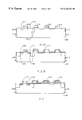
- FIG. 1A to FIG. 1G depicts the process flow of a preferred embodiment according to the present invention in cross-sectional views
- FIGS. 1A-1G the process flow of one preferred embodiment according to the present invention is depicted in cross-sectional views. These drawings merely show several key steps in sequential processes.
- a substrate 200 comprises a logic region 200 I and a DRAM region 200 II.
- the logic region 200 I there are a gate structure 204 on the substrate 200 , a source region 206 and a drain region 208 in the substrate 200 .
- the gate structure 204 consists of a silicon nitride layer as the topmost layer, a silicide layer, a polysilicon layer, and a gate oxide layer as the bottommost layer.
- isolation devices such as shallow trench isolations 202 A and 202 B, are formed at the outermost sides of the source region 206 and the drain region 208 .
- the DRAM region 200 II there are a multitude of transistor structures 210 on the substrate 200 and isolation devices, such as shallow trench isolations 202 C and co-used one 202 B at the sides of the transistor structures 210 .
- a salicide block layer 213 is formed to cover the surface of the DRAM region 200 II.
- a silicide layer 212 such as a TiSi 2 layer, is formed on the surface of the source region 206 and the drain region 208 of the logic region 200 I.
- the silicide layer 212 can reduce the sheet resistance of the source region 206 and the drain region 208 .
- a silicon nitride layer 214 is formed to cover the surfaces of both the logic region 200 I and the DRAM region 200 II.
- the silicon nitride layer 214 is formed by a chemical vapor deposition method and has a thickness about the range of 300 and 500 angstroms.
- the silicon nitride layer 214 is used as an etching stop layer during the formation of borderless contact windows.
- a photoresist film 216 first covers the logic region 200 I to expose the DRAM region 200 II.
- the photoresist film 216 is formed by the method of conventional spin coating. Then the silicon nitride layer 214 on the surface of the DRAM region 200 II is removed to expose the salicide block layer 213 of the DRAM region 200 II.
- the photoresist film 216 is removed by any suitable method.
- An inter-poly dielectric layer 218 is formed on the surfaces of both the logic region 200 I and the DRAM region 200 II.
- a pattern (not shown) is transferred into the inter-poly dielectric layer 218 to form a contact hole in the inter-poly dielectric layer 218 on the DRAM_region 200 II.
- a self-aligned bit-line contact window 220 is formed on the DRAM region 200 II by any suitably conventional methods, shown in FIG. 1 E.
- another inter-poly dielectric layer 222 is first formed on the surfaces of both the login region 200 I and the DRAM region 200 II.
- another contact hole is defined in the DRAM region 200 II and then a self-aligned node contact window 224 is formed in the DRAM region 200 II, shown in FIG. 1 F.
- the self-aligned node contact window 224 is at the side of the self-aligned bit-line contact window 220 and separated by one of the transistor structures 210 .
- an inter-level dielectric (ILD) layer 226 is first deposited on the surfaces of both the login region 200 I and the DRAM region 200 II. Then the inter-level dielectric layer 226 is planarized by chemical mechanic polishing. Multitudes of contact holes are defined in the logic region 200 I and then multitudes of borderless contact windows 228 , 232 and a contact window 230 are formed in the logic region 200 I. The contact window 230 is directly contacted with the gate structure 204 . The borderless contact windows 228 and 232 are contacted with the substrate 200 .
- a metallic layer (not shown) is first formed on the surfaces of both the logic region 200 I and the DRAM region 200 II and is then etched to form multitudes of metallic nodes 240 thereon, shown in FIG. 1 G. The metallic nodes 240 in the logic region 200 I are coupled to the borderless contact windows 228 , 232 and the contact window 230 .
- the silicon nitride layer 214 in the DRAM region 200 II is first removed before the formation of the contact hole for the self-aligned bit-line contact window 220 . It is advantageous for the formation of the self-aligned bit-line contact window 220 to avoid etching a multi-layer structure that may consist of the inter-poly dielectric layer 218 , the silicon nitride layer 214 , and the salicide block layer 213 . Furthermore, the short circuit of the transistor structure 210 in the DRAM region 200 II is reduced during the etching process for formation of the self-aligned bit-line contact window 220 .
Landscapes
- Engineering & Computer Science (AREA)
- Manufacturing & Machinery (AREA)
- Semiconductor Memories (AREA)
- Internal Circuitry In Semiconductor Integrated Circuit Devices (AREA)
Abstract
Description
Claims (12)
Priority Applications (2)
| Application Number | Priority Date | Filing Date | Title |
|---|---|---|---|
| TW088109876A TW436986B (en) | 1999-06-14 | 1999-06-14 | Embedded DRAM self-aligned contact with borderless contact and method for making the same |
| US09/375,518 US6426256B1 (en) | 1999-06-14 | 1999-08-17 | Method for fabricating an embedded DRAM with self-aligned borderless contacts |
Applications Claiming Priority (2)
| Application Number | Priority Date | Filing Date | Title |
|---|---|---|---|
| TW088109876A TW436986B (en) | 1999-06-14 | 1999-06-14 | Embedded DRAM self-aligned contact with borderless contact and method for making the same |
| US09/375,518 US6426256B1 (en) | 1999-06-14 | 1999-08-17 | Method for fabricating an embedded DRAM with self-aligned borderless contacts |
Publications (1)
| Publication Number | Publication Date |
|---|---|
| US6426256B1 true US6426256B1 (en) | 2002-07-30 |
Family
ID=26666703
Family Applications (1)
| Application Number | Title | Priority Date | Filing Date |
|---|---|---|---|
| US09/375,518 Expired - Lifetime US6426256B1 (en) | 1999-06-14 | 1999-08-17 | Method for fabricating an embedded DRAM with self-aligned borderless contacts |
Country Status (2)
| Country | Link |
|---|---|
| US (1) | US6426256B1 (en) |
| TW (1) | TW436986B (en) |
Cited By (3)
| Publication number | Priority date | Publication date | Assignee | Title |
|---|---|---|---|---|
| US20050106887A1 (en) * | 2003-11-17 | 2005-05-19 | Yi-Nan Chen | Method for formimg contact holes |
| US20070172964A1 (en) * | 2006-01-11 | 2007-07-26 | Cheng-Tyng Yen | Method of forming self-aligned contact via for magnetic random access memory |
| US11251189B2 (en) | 2009-02-09 | 2022-02-15 | Longitude Flash Memory Solutions Ltd. | Gate fringing effect based channel formation for semiconductor device |
Citations (8)
| Publication number | Priority date | Publication date | Assignee | Title |
|---|---|---|---|---|
| US4966870A (en) * | 1988-04-14 | 1990-10-30 | International Business Machines Corporation | Method for making borderless contacts |
| US5668035A (en) * | 1996-06-10 | 1997-09-16 | Taiwan Semiconductor Manufacturing Company Ltd. | Method for fabricating a dual-gate dielectric module for memory with embedded logic technology |
| US5858831A (en) * | 1998-02-27 | 1999-01-12 | Vanguard International Semiconductor Corporation | Process for fabricating a high performance logic and embedded dram devices on a single semiconductor chip |
| US5960318A (en) * | 1995-10-27 | 1999-09-28 | Siemens Aktiengesellschaft | Borderless contact etch process with sidewall spacer and selective isotropic etch process |
| US5998251A (en) * | 1997-07-19 | 1999-12-07 | United Microelectronics Corp. | Process and structure for embedded DRAM |
| US6017790A (en) * | 1998-07-06 | 2000-01-25 | United Microelectronics Corp. | Method of manufacturing embedded dynamic random access memory |
| US6025255A (en) * | 1998-06-25 | 2000-02-15 | Vanguard International Semiconductor Corporation | Two-step etching process for forming self-aligned contacts |
| US6072237A (en) * | 1996-03-15 | 2000-06-06 | Taiwan Semiconductor Manufacturing Company | Borderless contact structure |
-
1999
- 1999-06-14 TW TW088109876A patent/TW436986B/en not_active IP Right Cessation
- 1999-08-17 US US09/375,518 patent/US6426256B1/en not_active Expired - Lifetime
Patent Citations (8)
| Publication number | Priority date | Publication date | Assignee | Title |
|---|---|---|---|---|
| US4966870A (en) * | 1988-04-14 | 1990-10-30 | International Business Machines Corporation | Method for making borderless contacts |
| US5960318A (en) * | 1995-10-27 | 1999-09-28 | Siemens Aktiengesellschaft | Borderless contact etch process with sidewall spacer and selective isotropic etch process |
| US6072237A (en) * | 1996-03-15 | 2000-06-06 | Taiwan Semiconductor Manufacturing Company | Borderless contact structure |
| US5668035A (en) * | 1996-06-10 | 1997-09-16 | Taiwan Semiconductor Manufacturing Company Ltd. | Method for fabricating a dual-gate dielectric module for memory with embedded logic technology |
| US5998251A (en) * | 1997-07-19 | 1999-12-07 | United Microelectronics Corp. | Process and structure for embedded DRAM |
| US5858831A (en) * | 1998-02-27 | 1999-01-12 | Vanguard International Semiconductor Corporation | Process for fabricating a high performance logic and embedded dram devices on a single semiconductor chip |
| US6025255A (en) * | 1998-06-25 | 2000-02-15 | Vanguard International Semiconductor Corporation | Two-step etching process for forming self-aligned contacts |
| US6017790A (en) * | 1998-07-06 | 2000-01-25 | United Microelectronics Corp. | Method of manufacturing embedded dynamic random access memory |
Cited By (5)
| Publication number | Priority date | Publication date | Assignee | Title |
|---|---|---|---|---|
| US20050106887A1 (en) * | 2003-11-17 | 2005-05-19 | Yi-Nan Chen | Method for formimg contact holes |
| US7105453B2 (en) * | 2003-11-17 | 2006-09-12 | Nanya Technology Corporation | Method for forming contact holes |
| US20070172964A1 (en) * | 2006-01-11 | 2007-07-26 | Cheng-Tyng Yen | Method of forming self-aligned contact via for magnetic random access memory |
| US11251189B2 (en) | 2009-02-09 | 2022-02-15 | Longitude Flash Memory Solutions Ltd. | Gate fringing effect based channel formation for semiconductor device |
| US11950412B2 (en) | 2009-02-09 | 2024-04-02 | Longitude Flash Memory Solutions Ltd. | Gate fringing effect based channel formation for semiconductor device |
Also Published As
| Publication number | Publication date |
|---|---|
| TW436986B (en) | 2001-05-28 |
Similar Documents
| Publication | Publication Date | Title |
|---|---|---|
| US6022776A (en) | Method of using silicon oxynitride to improve fabricating of DRAM contacts and landing pads | |
| JP4911838B2 (en) | Semiconductor device and manufacturing method thereof | |
| US6274409B1 (en) | Method for making a semiconductor device | |
| KR20050029432A (en) | Method for fabrication of semiconductor device capable of protecting attack by wet cleaning | |
| US6072241A (en) | Semiconductor device with self-aligned contact and its manufacture | |
| US7105882B2 (en) | Semiconductor device memory cell | |
| US5580811A (en) | Method for the fabrication of a semiconductor memory device having a capacitor | |
| US6300178B1 (en) | Semiconductor device with self-aligned contact and manufacturing method thereof | |
| US6159844A (en) | Fabrication of gate and diffusion contacts in self-aligned contact process | |
| US5723374A (en) | Method for forming dielectric spacer to prevent poly stringer in stacked capacitor DRAM technology | |
| US6479355B2 (en) | Method for forming landing pad | |
| US20070212831A1 (en) | Method for manufacturing semiconductor device having plural electroconductive plugs | |
| US6372641B1 (en) | Method of forming self-aligned via structure | |
| US6426256B1 (en) | Method for fabricating an embedded DRAM with self-aligned borderless contacts | |
| US6207988B1 (en) | Semiconductor device and method for fabricating the same | |
| US6316311B1 (en) | Method of forming borderless contact | |
| KR100475715B1 (en) | MML Semiconductor Device Manufacturing Method | |
| JPH1197529A (en) | Method for manufacturing semiconductor device | |
| JP3172229B2 (en) | Method for manufacturing semiconductor device | |
| KR100469883B1 (en) | Semiconductor device fabricating method | |
| KR100704132B1 (en) | Semiconductor device having self-aligned contact and landing pad structure and method for forming same | |
| US7799676B2 (en) | Method of manufacturing a contact structure to avoid open issue | |
| KR100537187B1 (en) | Method for fabrication of semiconductor device | |
| US20050158972A1 (en) | Method for manufacturing bit line contact structure of semiconductor memory | |
| US20030047789A1 (en) | Semiconductor device and method of manufacturing the same |
Legal Events
| Date | Code | Title | Description |
|---|---|---|---|
| AS | Assignment |
Owner name: UNITED MICROELECTRONICS CORP., TAIWAN Free format text: ASSIGNMENT OF ASSIGNORS INTEREST;ASSIGNOR:CHEN, TUNG-PO;REEL/FRAME:010189/0867 Effective date: 19990719 |
|
| AS | Assignment |
Owner name: THERMO BIOSTAR INC., COLORADO Free format text: CHANGE OF NAME;ASSIGNOR:BIOSTAR, INC.;REEL/FRAME:012189/0506 Effective date: 20001027 |
|
| STCF | Information on status: patent grant |
Free format text: PATENTED CASE |
|
| FPAY | Fee payment |
Year of fee payment: 4 |
|
| FEPP | Fee payment procedure |
Free format text: PAYOR NUMBER ASSIGNED (ORIGINAL EVENT CODE: ASPN); ENTITY STATUS OF PATENT OWNER: LARGE ENTITY |
|
| FPAY | Fee payment |
Year of fee payment: 8 |
|
| AS | Assignment |
Owner name: AISAWA TECHNOLOGIES, LLC, DELAWARE Free format text: ASSIGNMENT OF ASSIGNORS INTEREST;ASSIGNOR:UNITED MICROELECTRONICS CORP.;REEL/FRAME:024723/0724 Effective date: 20100520 |
|
| FPAY | Fee payment |
Year of fee payment: 12 |