US6414772B2 - Method and apparatus for transmitting a wavelength division multiplexed (WDM) signal through an optical transmission line to reduce the effects of stimulated Brillouin scattering (SBS) - Google Patents
Method and apparatus for transmitting a wavelength division multiplexed (WDM) signal through an optical transmission line to reduce the effects of stimulated Brillouin scattering (SBS) Download PDFInfo
- Publication number
- US6414772B2 US6414772B2 US09/035,077 US3507798A US6414772B2 US 6414772 B2 US6414772 B2 US 6414772B2 US 3507798 A US3507798 A US 3507798A US 6414772 B2 US6414772 B2 US 6414772B2
- Authority
- US
- United States
- Prior art keywords
- signal
- transmission line
- light
- optical transmission
- wdm
- Prior art date
- Legal status (The legal status is an assumption and is not a legal conclusion. Google has not performed a legal analysis and makes no representation as to the accuracy of the status listed.)
- Expired - Fee Related
Links
Images


Classifications
-
- H—ELECTRICITY
- H04—ELECTRIC COMMUNICATION TECHNIQUE
- H04B—TRANSMISSION
- H04B10/00—Transmission systems employing electromagnetic waves other than radio-waves, e.g. infrared, visible or ultraviolet light, or employing corpuscular radiation, e.g. quantum communication
- H04B10/25—Arrangements specific to fibre transmission
- H04B10/2507—Arrangements specific to fibre transmission for the reduction or elimination of distortion or dispersion
- H04B10/2537—Arrangements specific to fibre transmission for the reduction or elimination of distortion or dispersion due to scattering processes, e.g. Raman or Brillouin scattering
Definitions
- the present invention relates to the transmission of a wavelength division multiplexed (WDM) signal through an optical fiber transmission line to reduce or eliminate the effects of stimulated Brillouin scattering (SBS).
- WDM wavelength division multiplexed
- Optical communication systems using fiber optical transmission lines are being used to transmit relatively large amounts of information.
- a light source produces light which is then modulated with data.
- the modulated light is input to, and transmitted through, an optical fiber transmission line.
- a receiver receives the modulated light from the optical fiber transmission line, and demodulates the light to obtain the data.
- SBS stimulated Brillouin scattering
- SBS refers to a phenomenon in which a nonlinear effect occurs in an optical fiber transmission line when a coherent light from a light source is input to the optical fiber transmission line at a higher intensity than a predetermined SBS threshold level, and the optical incident power is progressively increased.
- SBS a light having higher light intensity is returned to the light source. This returned light has an undesirable effect on the light source.
- SBS has a severely negative influence when the light source is a semiconductor laser and an optical fiber amplifier is used to amplify the light produced by the semiconductor laser.
- the intensity of light produced by a light source and input to an optical fiber transmission line is limited by the SBS threshold level of the optical fiber transmission line, thereby limiting the transmission distance.
- the intensity of light produced by a light source is below the SBS threshold level. See, for example, U.S. Pat. No. 4,560,246.
- the optical frequency or phase of the optical signal input to an optical transmission line is modulated to spread the coherent optical spectrum, to thereby suppress SBS. See, for example, “Nonlinear fiber optics” by Govind P. Agrawal, published by the Academic Press, Inc., pages 268 and 269.
- WDM wavelength division multiplexing
- WDM wavelength division multiplexing
- a plurality of light signals, each modulated with information is combined into a wavelength division multiplexed (WDM) light.
- WDM light is then transmitted through a single optical fiber (an optical fiber transmission line) to a receiver.
- the receiver splits the WDM light into the individual light signals, so that the individual light signals can be detected. In this manner, a communication system can transfer a relatively large amount of data over a single optical fiber.
- the above-described conventional techniques can be used to suppress SBS.
- the light signals in the WDM signal can be set at an intensity which is lower than the SBS threshold level of the optical fiber.
- the frequency or phase of light signals produced by a light source can be modulated to suppress SBS.
- the intensity of a light signal produced by a light source is limited since it must be below the SBS threshold level.
- the intensity per light signal will likely be further reduced, thereby reducing the transmission distance of the WDM signal.
- the foregoing objects of the present invention are achieved by providing and apparatus and method for transmitting a wavelength division multiplexed (WDM) signal through an optical fiber transmission line.
- the WDM signal includes a plurality of light signals multiplexed together.
- the WDM signal is transmitted to the optical transmission line so that the intensity per light signal is higher than an intensity threshold at which stimulated Brillouin scattering (SBS) occurs for a single light signal individually transmitted to the optical transmission line.
- SBS stimulated Brillouin scattering
- the WDM signal includes at least six light signals multiplexed together
- the intensity of each light signal can be higher than the intensity threshold at which SBS occurs for a single light signal individually transmitted to the optical transmission line.
- Objects of the present invention are also achieved by providing an optical communication system which suppresses SBS.
- At least six light sources each produce a respective, corresponding light signal.
- the light signal produced by each respective light source is at a different wavelength than the light signals produced by the other light sources.
- At least six modulators correspond, respectively, to the at least six light sources. Each modulator modulates the light signal produced by the corresponding light source.
- a multiplexer multiplexes the modulated light signals into a wavelength division multiplexed (WDM) signal.
- WDM wavelength division multiplexed
- the WDM signal is transmitted through the optical transmission line so that the intensity per light signal is higher than an intensity threshold at which stimulated Brillouin scattering (SBS) occurs for a single light signal individually transmitted to the optical transmission line.
- SBS stimulated Brillouin scattering
- FIG. 1 is a diagram illustrating an optical communication system which measures a characteristic of an optical signal to suppress SBS, according to an embodiment of the present invention.
- FIG. 2 is a graph showing the SBS threshold level for each semiconductor laser of the optical communication system in FIG. 1, according to an embodiment of the present invention.
- FIG. 3 is a graph showing the SBS threshold level of the optical communication system in FIG. 1 when the number of wavelength multiplexed light signals is increased, according to an embodiment of the present invention.
- FIG. 4 is a diagram showing the SBS threshold level of the optical communication system in FIG. 1 when a coded pattern is changed, according to an embodiment of the present invention.
- FIG. 5 is an additional diagram showing the SBS threshold level of the optical communication system in FIG. 1 when a coded pattern is changed, according to an embodiment of the present invention.
- FIGS. 6 (A), 6 (B), 6 (C), 6 (D), 6 (E), 6 (F) and 6 (G) are graphs illustrating spectrum characteristics of the semiconductor lasers illustrated in FIG. 1, according to an embodiment of the present invention.
- FIGS. 7 (A), 7 (B), 7 (C) and 7 (D) are graphs showing spectrum characteristics depending on different signal patterns, according to an embodiment of the present invention.
- FIGS. 8 (A), 8 (B), 8 (C) and 8 (D) are graphs showing the characteristic of a wavelength W 1 when the output of multiplexed wavelengths is increased, according to an embodiment of the present invention.
- FIGS. 9 (A), 9 (B), 9 (C) and 9 (D) are graphs illustrating the characteristic of a wavelength W 5 when the output of multiplexed wavelengths is increased, according to an embodiment of the present invention.
- FIGS. 10 (A), 10 (B), 10 (C) and 10 (D) are graphs showing the characteristic of a wavelength W 8 when the output of multiplexed wavelengths is increased, according to an embodiment of the present invention.
- FIG. 11 is a graph showing the characteristic of a wavelength W 3 , according to an embodiment of the present invention.
- FIGS. 12 (A), 12 (B), 12 (C); 12 (D), 12 (E) and 12 (F) are graphs showing the characteristic of four-photon mixing of an output of multiplexed wavelengths, according to an embodiment of the present invention.
- FIG. 13 is a diagram illustrating a transmission side of an optical communication system, according to an embodiment of the present invention.
- FIG. 14 is a diagram illustrating a reception side of an optical communication system, according to an embodiment of the present invention.
- FIG. 15 (prior art) is a table illustrating the generation of pseudo-random patterns using shift registers connected in stages.
- FIG. 16 (prior art) is a diagram illustrating a pattern generating circuit in accordance with the table of FIG. 15 .
- FIG. 1 is a diagram illustrating an optical communication system which measures a characteristic of an optical signal to suppress SBS, according to an embodiment of the present invention.
- semiconductor lasers (LD) 1 — 1 through 1 - 8 each emit a respective light signal.
- Each light signal is preferably at a different wavelength than the other light signals, so that each light signal represents a different channel for transmitting information.
- An optical coupler (CPL) 2 multiplexes the light signal into a wavelength division multiplexed (WDM) signal, and an optical modulator (LN Modulator) 3 modulates the WDM signal.
- WDM wavelength division multiplexed
- LN Modulator optical modulates the WDM signal.
- optical modulator 3 digitally modulates the amplitude of a pseudo-random pattern PN 23 using an NRZ signal from a pulse pattern generator (PPG) 3 - 1 .
- PPG pulse pattern generator
- a polarization scrambler (SCR) 4 passes the WDM signal without scrambling.
- Optical amplifiers 5 - 1 and 5 - 2 amplify the WDM signal and then transmit it to an optical transmission line 6 made of, for example, pure silica fiber.
- Optical transmission line 6 has a length of, for example, 140 Km.
- the intensity of light input to optical transmission line 6 is detected by a light intensity monitor (power meter) 8 - 2 through an attenuator 7 - 2 . Moreover, if SBS occurs, light will be returned back through optical transmission line 6 . The returned light is detected by a light intensity monitor (power meter) 8 - 1 through an attenuator 7 - 1 .
- FIG. 1 also illustrates an LN type E/O module 3 - 3 and a pulse pattern generator (PPG) 3 - 2 , which will be described in more detail further below.
- PPG pulse pattern generator
- FIG. 2 is a graph showing the SBS threshold level for semiconductor lasers 1 - 1 , 1 - 2 , 1 - 3 , 1 - 4 , 1 - 5 , 1 - 6 , 1 - 7 and 1 - 8 , according to an embodiment of the present invention.
- the horizontal axis represents P IN , that is, the intensity detected by light intensity monitor 8 - 2 .
- the vertical axis represents P BACK /P IN , that is, the ratio of the intensity detected by light intensity monitor 8 - 1 to the intensity detected by light intensity monitor 8 - 2 .
- the wavelength of the light signal produced by semiconductor laser 1 - 1 is, for example, 1553.9 nm and is hereinafter referred to as “W 1 ”.
- the wavelength of the light signal produced by semiconductor laser 1 - 2 is, for example, 1554.9 nm and is hereinafter referred to as “W 2 ”.
- the wavelength of the light signal produced by semiconductor laser 1 - 3 is, for example, 1555.9 nm and is hereinafter referred to as “W 3 ”.
- the wavelength of the light signal produced by semiconductor laser 1 - 4 is, for example, 1556.9 nm and is hereinafter referred to as “W 4 ”.
- the wavelength of the light signal produced by semiconductor laser 1 - 5 is, for example, 1557.9 nm and is hereinafter referred to as “W 5 ”.
- the wavelength of the light signal produced by semiconductor laser 1 - 6 is, for example, 1558.9 nm and is hereinafter referred to as “W 6 ”.
- the wavelength of the light signal produced by semiconductor laser 1 - 7 is, for example, 1559.9 nm and is hereinafter referred to as “W 7 ”.
- the wavelength of the light signal produced by semiconductor laser 1 - 8 is, for example, 1560.9 nm and is hereinafter referred to as “W 8 ”.
- the SBS threshold level of the light signals produced by the semiconductor lasers is not fixed, but is in a range from 8 dBm to 11 dBm. Moreover, each wavelength exhibits a similar shaped characteristic curve. As previously described, the SBS threshold level is the level of the light signal which causes light to be returned back to the semiconductor laser through optical transmission line 6 .
- FIG. 3 is a graph showing the SBS threshold level of the optical communication system in FIG. 1 when the number of wavelength multiplexed light signals is increased, according to an embodiment of the present invention. More specifically, FIG. 3 shows the case in which a plurality of light signals at different wavelengths are added one by one, starting with semiconductor laser 1 - 1 under the conditions shown in FIG. 2 .
- W 1 indicates the case where semiconductor laser 1 - 1 singly emits a light signal.
- W 1 -W 2 indicates the case in which light signals are emitted from both semiconductor lasers 1 - 1 and 1 - 2 .
- W 1 -W 3 indicates the case in which light signals are emitted from all of semiconductor lasers 1 - 1 through 1 - 3 .
- semiconductor lasers are increased one by one to measure the SBS threshold level of each of the combinations up to W 1 -W 8 .
- the SBS threshold level (that is, the level of the light input into optical transmission line 6 which causes light to be returned back to the semiconductor lasers) of W 1 is approximately 8 dBm.
- the SBS threshold level of W 1 -W 2 is approximately 10 dBm with 7 dBm per wave.
- the SBS threshold level of W 1 -W 3 is approximately 13 dBm with 8 dBm per wave.
- the SBS threshold level of W 1 -W 4 is approximately 14 dBm with 8 dBm per wave.
- the SBS threshold level of W 1 -W 5 is approximately 15 dBm with 8 dBm per wave.
- the SBS threshold level of W 1 -W 6 is approximately 16 dBm with 8.2 dBm per wave.
- the SBS threshold level of W 1 -W 7 is approximately 16 dBm with 7.5 dBm per wave.
- the SBS threshold level of W 1 -W 8 is approximately 16 dBm with 7 dBm per
- the above-described SBS threshold levels are directly identifiable from FIG. 3 .
- the SBS threshold level of W 1 -W 2 is approximately 10 dBm.
- This SBS threshold level can be seen from FIG. 3, where light begins returning at approximately 10 dBm for W 1 -W 2 .
- the above-described “per wave” values (such as the 7 dBm “per wave” value for W 1 -W 2 ) can easily be determined from the data in FIG. 3 .
- the slope of the corresponding characteristic curve decreases. More specifically, the rate of increase of SBS decreases as the number of multiplexed light signals is set at six (6) or more.
- the rate of increase for the value of a returned light from optical transmission line 6 exceeding the SBS threshold level can be reduced by setting the number of multiplexed light signals, or wavelengths, to six (6) or more, thereby suppressing SBS.
- FIG. 4 is a diagram showing the SBS threshold level of the optical communication system in FIG. 1 when a coded pattern is changed, according to an embodiment of the present invention.
- 1010 W 1 - 8 indicates the state in which a WDM signal having the wavelengths W 1 to W 8 is modulated by optical modulator 3 according to the alternating signal of * 1010 * from pulse pattern generator 3 - 1 shown in FIG. 1 .
- PN 7 W 1 -W 8 indicates the state in which a WDM signal having the wavelengths W 1 to W 8 is modulated according to the signal of the pseudo-random pattern PN 7 .
- PN 23 W 1 -W 8 indicates the state in which a WDM signal having the wavelengths W 1 to W 8 is modulated according to the signal of the pseudo-random pattern PN 23 .
- 1010 W 1 indicates the state in which a light having the wavelength W 1 is modulated according to the alternating signal of * 1010 *.
- PN 23 W 1 indicates the state in which a light having the wavelength W 1 is modulated according to the signal of the pseudo-random pattern PN 23 .
- a longer period pseudo-random pattern produces a higher SBS suppression effect with a fixed number of multiplexed light signals, or wavelengths.
- FIG. 5 is an additional diagram showing the SBS threshold level of the optical communication system in FIG. 1 when a coded pattern is changed, according to an embodiment of the present invention.
- FIG. 5 shows the case in which, referring to FIG. 1, semiconductor lasers 1 - 1 through 1 - 7 produce light signals at wavelengths W 1 through W 7 , respectively, and which are modulated by E/O module 3 - 3 .
- E/O module 3 - 3 generates a light with the wavelength W 0 (1552.0 nm) using a common coding pattern and a pattern generated by pulse pattern generator 3 - 2 .
- the modulated light signals are combined by optical coupler 2 - 2 and then provided to optical transmission line 6 .
- W 0 1010 W 1 -W 7 PN 23 indicates that W 0 is modulated using the alternating signal * 1010 *, and W 1 through W 7 are modulated using the pseudo-random pattern PN 23 .
- W 0 PN 23 W 1 -W 7 PN 23 indicates that all of W 0 and W 1 through W 7 are modulated using the pseudo-random pattern PN 23 .
- W 0 1010 W 1 -W 7 1010 indicates that all of W 0 and W 1 through W 7 are modulated using the alternating signal * 1010 *.
- W 0 PN 23 W 1 -W 7 1010 indicates that W 0 is modulated using the pseudo-random pattern PN 23 , and W 1 through W 7 are modulated using the alternating signal * 1010 *.
- FIGS. 6 (A), 6 (B), 6 (C), 6 (D), 6 (E), 6 (F) and 6 (G) are graphs illustrating the spectrum characteristics of semiconductor lasers illustrated in FIG. 1, according to an embodiment of the present invention. More specifically, FIGS. 6 (A), 6 (B), 6 (C), 6 (D), 6 (E), 6 (F) and 6 (G) are graphs illustrating, respectively, the spectrum measured when a single one of the wavelengths W 1 , W 2 , W 3 , W 5 , W 6 , W 7 and W 8 is emitted from the corresponding semiconductor laser 1 - 1 through 1 - 8 .
- the wavelength of semiconductor laser 1 - 4 is unstable, so a result cannot be provided for W 4 . Therefore, no graph is illustrated for the wavelength W 4 .
- the total input power of the eight multiplexed light signals (W 1 to W 8 ) to optical transmission line 6 was measured at 23 dBm.
- FIGS. 7 (A), 7 (B), 7 (C) and 7 (D) are graphs showing spectrums measured at the output end of optical transmission line 6 (140 km), and illustrating the difference in characteristics between different coding patterns when 23 dBm is input to optical transmission line 6 with eight (8) multiplexed light signals with wavelengths W 1 to W 8 , respectively.
- FIG. 7 (A) shows the spectrum of wavelength W 1 using the modulation signal PN 23 with eight multiplexed wavelengths from W 1 to W 8 .
- FIG. 7 (B) shows the spectrum of wavelength W 1 using the alternating signal * 1010 * with eight multiplexed wavelengths from W 1 to W 8 .
- FIG. 7 (C) shows the spectrum of wavelength W 8 using the modulation signal PN 23 with eight multiplexed wavelengths from W 1 to W 8 .
- FIG. 7 (D) shows the spectrum of wavelength W 8 using the modulation signal * 1010 * with eight multiplexed wavelengths from W 1 to W 8 .
- the spectrum obtained using the modulation signal PN 23 is about ten times more spread than the spectrum shown in FIGS. 6 (A), 6 (B), 6 (C), 6 (D), 6 (E), 6 (F) and 6 (G), and FIGS. 7 (B) and 7 (D).
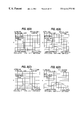
- FIGS. 8 (A), 8 (B), 8 (C) and 8 (D) are graphs showing the relationship between the spectrum of wavelength W 1 and the intensity of the light input to optical transmission line 6 when wavelengths W 1 through W 8 are multiplexed.
- FIG. 8 (A) indicates an optical input of 10 dBm to optical transmission line 6 .
- FIG. 8 (B) indicates a total optical input power of eight multiplexed light signals W 1 to W 8 of 19 dBm to optical transmission line 6 .
- FIG. 8 (C) indicates a total optical input power of 21 dBm to optical transmission line 6 .
- FIG. 8 (D) indicates a total optical input power of 23 dBm to optical transmission line 6 .
- FIGS. 9 (A), 9 (B), 9 (C) and 9 (D) are graphs showing the relationship between the spectrum of wavelength W 5 and the intensity of the light input to optical transmission line 6 when wavelengths W 1 through W 8 are multiplexed.
- FIG. 9 (A) indicates an optical input of 10 dBm to optical transmission line 6 .
- FIG. 9 (B) indicates an optical input of 19 dBm to optical transmission line 6 .
- FIG. 9 (C) indicates an optical input of 21 dBm to optical transmission line 6 .
- FIG. 9 (D) indicates an optical input of 23 dBm to optical transmission line 6 .
- FIGS. 10 (A), 10 (B), 10 (C) and 10 (D) are graphs showing the relationship between the spectrum of wavelength W 8 and the intensity of the light input to optical transmission line 6 when wavelengths W 1 through W 8 are multiplexed.
- FIG. 10 (A) indicates an optical input of 10 dBm to optical transmission line 6 .
- FIG. 10 (B) indicates an optical input of 19 dBm to optical transmission line 6 .
- FIG. 10 (C) indicates an optical input of 21 dBm to optical transmission line 6 .
- FIG. 10 (D) indicates an optical input of 23 dBm to optical transmission line 6 .
- the spectrum of each wavelength is spread.
- the spectrum is spread toward a longer wavelength about the line spectrum with the shortest wavelength W 1 .
- the spectrum is spread toward a shorter wavelength about the line spectrum with the longest wavelength W 8 .
- the spectrum is spread toward both sides about the line spectrum with the central wavelength W 5 .
- FIG. 11 is a graph illustrating the spectrum of wavelength W 3 with a light intensity 21 dBm of the WDM signal input to optical transmission line 6 .
- the tendency of the shortest wavelength W 1 and the central wavelength W 5 can be determined. That is, the spectrum is spread toward a longer wavelength about the line spectrum.
- a longer wavelength spreads its spectrum toward a shorter wavelength
- a shorter wavelength spreads its spectrum toward a longer wavelength.
- the central multiplexed-wavelength functioning as a boundary between the longer and shorter wavelengths and spreads its spectrum toward both of shorter and longer wavelengths when the output of the wavelength-multiplexed light signals of semiconductor lasers 1 - 1 and 1 - 8 are increased.
- FIGS. 12 (A), 12 (B), 12 (C), 12 (D), 12 (E) and 12 (F) are graphs showing the wavelength characteristics when one of the multiplexed wavelengths W 1 to W 8 is stopped. More specifically, FIG. 12 (A) indicates the spectrum when wavelength W 1 is stopped with an input of 15 dBm to optical transmission line 6 .
- FIG. 12 (B) indicates the spectrum when wavelength W 5 is stopped with an input of 15 dBm to optical transmission line 6 .
- FIG. 12 (C) indicates the spectrum when wavelength W 8 is stopped with an input of 15 dBm to optical transmission line 6 .
- FIG. 12 (D) indicates the spectrum when wavelength W 1 is stopped with an input of 23 dBm to optical transmission line 6 .
- FIG. 12 (E) indicates the spectrum when wavelength W 5 is stopped with an input of 23 dBm to optical transmission line 6 .
- FIG. 12 (F) indicates the spectrum when wavelength W 8 is stopped with an input of 23 dBm to optical transmission line 6 .
- an SBS-occurring threshold is determined by a light intensity per wave and a spectrum line width.
- the spectrum line width of a transmission signal tends to spread. It is predicted herein that the spectrum line width of a light from a semiconductor laser is spread by nonlinear effect (such as, for example, a cross-phase moderation: XPM) in optical transmission line 6 , and SBS is suppressed.
- nonlinear effect such as, for example, a cross-phase moderation: XPM
- the spectrum line width should be increased at an early stage after the light is input to optical transmission line 6 .
- FIG. 13 is a diagram illustrating a transmission side of an optical communication system, according to an embodiment of the present invention.
- the optical communication system includes optical modulators 31 through 38 (although only optical modulators 31 and 38 are shown), drivers 3 - 41 through 3 - 48 (although only driver 3 - 41 and 3 - 48 are shown), scramblers 3 - 51 through 3 - 58 (although only scramblers 3 - 51 and 3 - 58 are shown), attenuators 10 - 1 through 10 - 8 (although only attenuators 10 - 1 and 10 - 8 are shown), an optical isolator 8 , optical amplifiers 5 - 1 and 5 - 2 , and a dispersion compensator 9 .
- the present invention is not intended to be limited to any specific configuration.
- the interval of the wavelengths from semiconductor lasers 1 - 1 through 1 - 8 is preferably set to a value equal to or smaller than 1 nm to enlarge the influence of the XPM.
- input signals to scramblers 3 - 51 through 3 - 58 are NRZ signals, to enlarge the influence of the XPM.
- a signal output from scrambler 3 - 51 is input to driver 3 - 41 for driving optical modulator 31 , and a light from semiconductor laser 1 - 1 is modulated by modulator 31 .
- the light is preferably digitally modulated in amplitude.
- the output from modulator 31 is input to attenuator 10 - 1 , and the output level is controlled by using the relationship between the level of a light from another semiconductor laser and a gain of an optical amplifier.
- the light produced by semiconductor lasers 1 - 2 through 1 - 8 is scrambled and processed in a similar manner as that for semiconductor laser 1 - 1 .
- An output from attenuator 10 - 1 is wavelength-multiplexed with an output from semiconductor lasers 1 - 2 through 1 - 8 by optical coupler 2 , to produce a WDM signal.
- the polarization of the WDM signal from optical coupler 2 is scrambled by polarization scrambler 4 , and then amplified by optical amplifier 5 - 1 .
- optical amplifier 5 - 1 An output from optical amplifier 5 - 1 is connected to optical amplifier 5 - 2 through optical isolator 8 .
- Optical amplifiers 5 - 1 and 5 - 2 each comprise an erbium doped fiber (EDF) and each amplifier preferably levels amplified bands by assigning different gains.
- the output from optical amplifier 5 - 2 is higher than the light intensity of the threshold level of SBS which occurs in optical transmission line 6 when light is transmitted with a single wavelength.
- Dispersion compensator 9 not only compensates for the dispersion of optical transmission line 6 but also intentionally generates a nonlinear effect by setting the type of dispersion compensator 9 and the amount of its dispersion compensation to a predetermined value so that the spreading of the width of the spectrum can be performed at an early stage after light is input to optical transmission line 6 .
- An effective dispersion compensator 9 can be, for example, a dispersion compensation fiber (DCF) or a dispersion shifted fiber (DSF) indicating the largest nonlinear effect and guaranteeing dispersion compensation of an optical transmission line.
- DCF dispersion compensation fiber
- DSF dispersion shifted fiber
- FIG. 14 is a diagram illustrating a reception side of an optical communication system, according to an embodiment of the present invention.
- a WDM signal is transmitted through optical transmission line 6 and is amplified by a preamplifier 22 .
- a dispersion compensator 24 can be provided to compensate for dispersion.
- a demultiplexer 26 demultiplexes the WDM signal into individual signal lights which are detected by receivers 28 - 1 through 28 - 8 which can be, for example, PIN photodiodes, or APD diodes.
- receivers 28 - 1 through 28 - 8 can be, for example, PIN photodiodes, or APD diodes.
- SBS can be suppressed by setting the light intensity of a WDM signal transmitted through an optical transmission line to be higher than the light intensity at which SBS occurs for a single light transmitted through the optical transmission line. Furthermore, the SBS suppression effect can be improved by scrambling an input signal at stage 7 or longer period in a maximum period sequence. The SBS suppression effect can also be improved by using an input signal of NRZ, digitally modulating the optical amplitude, and shortening the wavelength interval to 1 nm or less.
- the above embodiments of the present invention illustrate an optical communication system having a specific number of semiconductor lasers, each producing a respective light signal.
- the present invention is not intended to be limited to a specific number of semiconductor lasers or a specific number of wavelength multiplexed signal lights.
- the present invention is not intended to be limited to the use of any specific type of light source.
- a WDM signal is transmitted to an optical transmission line so that the intensity per light signal is higher than an intensity threshold at which stimulated Brillouin scattering (SBS) occurs for a single light signal individually transmitted to the optical transmission line.
- SBS stimulated Brillouin scattering
- each semiconductor laser 1 - 1 through 1 - 8 can produce a respective light signal which is higher than the intensity threshold at which SBS occurs for a single light signal.
- These relatively high intensity light signals can then be combined into a relatively high intensity WDM signal which is transmitted through optical transmission line 6 .
- the present invention recognizes that SBS is substantially reduced or eliminated in this situation, especially when at least six (6) light signals are multiplexed together. This can be contrasted to conventional techniques which required each light signal in the WDM signal to be less than the intensity threshold at which SBS occurs for a single light signal.
- PN 7 or PN 23 Various of the above embodiments of the present invention relate to the use of pseudo-random patterns, such as those described above as PN 7 or PN 23 .
- Pseudo-random patterns are often generated in accordance with standard, well-known testing pattern guidelines, to provide a random pattern having a specific period. The generation of pseudo-random patterns is well-known by persons of skill in the art.
- pseudo random patterns are generated by various logic components, such as flip-flops, connected together to provide an appropriate pattern.
- pseudo-random pattern PN 7 refers to logical elements, such as flip-flops, connected together in seven (7) stages to produce a random pattern having a period of (2 7 ⁇ 1) bits.
- pseudo-random pattern PN 23 refers to logical elements connected together in twenty-three (23) stages to produce a random pattern having a period of (2 23 ⁇ 1) bits.
- Pseudo-random pattern PN 23 is a random pattern having a longer period than pseudo-random pattern PN 7 .
- a pattern can be described in relation to the number of stages for producing the pattern.
- a seven stage pattern is a pattern having a period of (2 7 ⁇ 1) bits.
- PN 7 is such a seven stage pattern.
- a pattern which is longer than a seven stage pattern would have more than seven stages and would have a period longer than (2 7 ⁇ 1) bits.
- PN 23 is pattern which is longer than PN 7 and therefore has a period longer than (2 7 ⁇ 1) bits.
- stage 7 or longer refers to patterns having a period of (2 7 ⁇ 1) bits or longer.
- FIG. 15 is a table illustrating the generation of pseudo-random patterns using shift registers connected in stages.
- FIG. 16 is a diagram illustrating a pattern generating circuit in accordance with the table of FIG. 15 .
- FIGS. 15 and 16 are included in the ANRITSU Pulse Pattern Generator MP1650A Instruction Book, Chapter 6, Principle of Operations, which is incorporated herein be reference.
- pseudo-random patterns can also be understood, for example, from the International Telecommunication Union (ITU), International Brass and Telephone Consultative Committee (CCITT), “Specification of Measuring Equipment, Error Performance Measuring Equipment Operating At The Primary Rate And Above”, Recommendation 0.151, October 1992, and also from the International Telecommunication Union (ITU), Telecommunication Standardization Sector of the ITU (ITU-T), “General requirements for instrumentation for performance measurements on digital transmission equipment”, Recommendation 0.150, May, 1996, which are incorporated herein by reference.
- ITU International Telecommunication Union
- CITT International Telegraph and Telephone Consultative Committee
- ITU-T Telecommunication Standardization Sector of the ITU
- Recommendation 0.150, May, 1996 which are incorporated herein by reference.
- a transmitter transmits a WDM signal to an optical transmission line.
- the various semiconductor lasers 1 - 1 through 1 - 8 together with optical coupler 2 , would constitute a transmitter which transmits a WDM signal.
- the various semiconductor lasers 1 - 1 through 1 - 8 , optical coupler 2 , and the various other elements connected between the semiconductor lasers and the optical coupler would together constitute a transmitter which transmits a WDM signal.
- the present invention is not intended to be limited to any specific configuration.
- a receiver receives a WDM signal from an optical transmission line.
- demultiplexer 26 and the various individual receivers 28 - 1 through 28 - 8 can together be considered to be a receiver which receives a WDM signal.
- an individual receiver such as receiver 28 - 1 , could possibly receive a WDM signal and would therefore be considered to be a receiver which receives a WDM signal. Therefore, there are many different configurations for a receiver which receives a WDM signal, and the present invention is not intended to be limited to any specific configuration.
- SBS is described as being related to the intensity level of light input to an optical transmission line. It should be noted that, generally, SBS is also dependent on the wavelength of the light. However, in optical communication systems employing WDM, the WDM bandwidth is relatively narrow so that the wavelength dependence of SBS can be ignored.
Applications Claiming Priority (3)
| Application Number | Priority Date | Filing Date | Title |
|---|---|---|---|
| JP5073897 | 1997-03-05 | ||
| JP09-050738 | 1997-03-05 | ||
| JP9-050738 | 1997-03-05 |
Publications (2)
| Publication Number | Publication Date |
|---|---|
| US20010010587A1 US20010010587A1 (en) | 2001-08-02 |
| US6414772B2 true US6414772B2 (en) | 2002-07-02 |
Family
ID=12867189
Family Applications (1)
| Application Number | Title | Priority Date | Filing Date |
|---|---|---|---|
| US09/035,077 Expired - Fee Related US6414772B2 (en) | 1997-03-05 | 1998-03-05 | Method and apparatus for transmitting a wavelength division multiplexed (WDM) signal through an optical transmission line to reduce the effects of stimulated Brillouin scattering (SBS) |
Country Status (3)
| Country | Link |
|---|---|
| US (1) | US6414772B2 (zh) |
| EP (1) | EP0863630A3 (zh) |
| CN (1) | CN1082753C (zh) |
Cited By (8)
| Publication number | Priority date | Publication date | Assignee | Title |
|---|---|---|---|---|
| US20010004289A1 (en) * | 1999-12-21 | 2001-06-21 | Lee Sang-Soo | Apparatus and method for stimulated brillouin scattering supression using supervisory channel |
| US6661815B1 (en) * | 2002-12-31 | 2003-12-09 | Intel Corporation | Servo technique for concurrent wavelength locking and stimulated brillouin scattering suppression |
| US20040156643A1 (en) * | 2003-02-11 | 2004-08-12 | Frederiksen Thomas R. | Optical transmitter with sbs suppression |
| US6781747B2 (en) * | 2001-06-21 | 2004-08-24 | Alcatel | Method for the amplification of wavelength division multiplex (WDM) signals in a WDM transmission system, as well as optical amplifier, optical amplifier system and WDM transmission system for it |
| US20040208565A1 (en) * | 2001-12-14 | 2004-10-21 | Nortel Networks Limited | Decorrelation of WDM signals |
| US20060067685A1 (en) * | 2004-09-28 | 2006-03-30 | Siemens Aktiengesellschaft | Method and arrangement for determining the dispersion of an optical transmission link |
| US20060251424A1 (en) * | 2005-05-04 | 2006-11-09 | Fitel Usa Corp. | Stabilized optical fiber continuum frequency combs using post-processed highly nonlinear fibers |
| US20090231681A1 (en) * | 2008-03-14 | 2009-09-17 | General Atomics | Optical system for reducing stimulated brillouin scattering by controllably changing polarization direction of an optical signal |
Families Citing this family (6)
| Publication number | Priority date | Publication date | Assignee | Title |
|---|---|---|---|---|
| DE19950880C1 (de) * | 1999-10-22 | 2001-06-28 | Torsten Gogolla | Verfahren und Fasersensor zur Korrektur von im Zuge ortsausgelöster Messungen aufgenommenen Brillouin-Spektren |
| EP1221776B1 (en) * | 2001-01-04 | 2004-09-15 | Alcatel | Optical fiber transmission system with enhanced total launchable optical power |
| JP3997890B2 (ja) * | 2001-11-13 | 2007-10-24 | 松下電器産業株式会社 | 送信方法及び送信装置 |
| EP1577704A4 (en) * | 2002-11-21 | 2008-01-02 | Furukawa Electric Co Ltd | LIGHT SOURCE OF OPTICAL TRANSMISSION SYSTEM, WAVEFORM CONFORMER, OPTICAL IMPULSE TRAIN GENERATOR, AND OPTICAL REPRODUCTION SYSTEM |
| CN100380225C (zh) * | 2002-11-21 | 2008-04-09 | 古河电气工业株式会社 | 光脉冲串发生装置 |
| CN1299160C (zh) * | 2004-04-29 | 2007-02-07 | 清华大学 | 一种用于光纤参量放大泵浦源的受激布里渊散射抑制方法 |
Citations (6)
| Publication number | Priority date | Publication date | Assignee | Title |
|---|---|---|---|---|
| US3705992A (en) | 1971-12-13 | 1972-12-12 | Bell Telephone Labor Inc | Broadband tunable raman-effect devices in optical fibers |
| US4168427A (en) | 1978-06-14 | 1979-09-18 | Bell Telephone Laboratories, Incorporated | Duplex optical communication system with reverse Rayleigh scattered power equalizer |
| US4560246A (en) | 1982-06-04 | 1985-12-24 | British Telecommunications | Optical transmission |
| US5515192A (en) * | 1992-03-19 | 1996-05-07 | Fujitsu Limited | Optical systems making use of phenomenon of stimulated brillouin scattering |
| US5559910A (en) * | 1994-06-06 | 1996-09-24 | Kokusai Denshin Denwa Kabushiki Kaisha | Wavelength division multiplexed optical fiber transmission equiptment |
| EP0758169A2 (en) | 1995-08-09 | 1997-02-12 | Nec Corporation | Wavelength division multiplexing optical transmission system and wavelength division multiplexing optical transmission method |
Family Cites Families (4)
| Publication number | Priority date | Publication date | Assignee | Title |
|---|---|---|---|---|
| JP3223562B2 (ja) * | 1992-04-07 | 2001-10-29 | 株式会社日立製作所 | 光送信装置、光伝送装置および光変調器 |
| US5555477A (en) * | 1992-04-08 | 1996-09-10 | Hitachi, Ltd. | Optical transmission system constructing method and system |
| US5587830A (en) * | 1993-05-28 | 1996-12-24 | Lucent Technologies Inc. | High capacity optical fiber network |
| US5513029A (en) * | 1994-06-16 | 1996-04-30 | Northern Telecom Limited | Method and apparatus for monitoring performance of optical transmission systems |
-
1998
- 1998-03-04 CN CN98106011A patent/CN1082753C/zh not_active Expired - Fee Related
- 1998-03-05 EP EP98103951A patent/EP0863630A3/en not_active Withdrawn
- 1998-03-05 US US09/035,077 patent/US6414772B2/en not_active Expired - Fee Related
Patent Citations (8)
| Publication number | Priority date | Publication date | Assignee | Title |
|---|---|---|---|---|
| US3705992A (en) | 1971-12-13 | 1972-12-12 | Bell Telephone Labor Inc | Broadband tunable raman-effect devices in optical fibers |
| US4168427A (en) | 1978-06-14 | 1979-09-18 | Bell Telephone Laboratories, Incorporated | Duplex optical communication system with reverse Rayleigh scattered power equalizer |
| US4560246A (en) | 1982-06-04 | 1985-12-24 | British Telecommunications | Optical transmission |
| US4560246B1 (en) | 1982-06-04 | 1998-06-09 | British Telecomm | Optical transmission |
| US5515192A (en) * | 1992-03-19 | 1996-05-07 | Fujitsu Limited | Optical systems making use of phenomenon of stimulated brillouin scattering |
| US5559910A (en) * | 1994-06-06 | 1996-09-24 | Kokusai Denshin Denwa Kabushiki Kaisha | Wavelength division multiplexed optical fiber transmission equiptment |
| EP0758169A2 (en) | 1995-08-09 | 1997-02-12 | Nec Corporation | Wavelength division multiplexing optical transmission system and wavelength division multiplexing optical transmission method |
| US5956166A (en) * | 1995-08-09 | 1999-09-21 | Nec Corporation | Wavelength division multiplexing optical transmission system and wavelength division multiplexing optical transmission method |
Non-Patent Citations (9)
| Title |
|---|
| "McGraw-Hill Dictionary of Scientific and Technical Terms", Third Edition, 1984, p. 1196. |
| "McGraw-Hill Encyclopedia of Science and Technology", 1960, p. 103. |
| "Series O: Specifications of Measuring Equipment, Equipment for the measurement of digital and analogue/digital parameters, General requirements for instrumentation for performance measurements on digital transmission equipment", ITU-T Recommendation 0.150, May 1996. |
| "Specification Of Measuring Equipment, Error Performance Measuring Equipment Operating At The Primary Rate and Above", The International Telegraph and Telephone Consultative Committee (CCITT), Recommendation 0.151, Oct. 1992. |
| John Bellamy, "Digital Telephony", published by John Wiley & Sons, Inc., 1982, p. 277-278. |
| P.B. Hansen, et al., "8 x 10 Gb/s WDM Repeaterless Transmission Over 352 km", IOOC 95, PD2-4, p. 27. |
| P.B. Hansen, et al., "8 × 10 Gb/s WDM Repeaterless Transmission Over 352 km", IOOC 95, PD2-4, p. 27. |
| Yamamoto et al., "Coherent Optical Fiber Transmission Systems", IEEE Journal Of Quantum Electronics, vol. QE-17, No. 6, Jun., 1981, pp. 919-935. |
| Yamamoto et al., "Coherent Optical Fiber Transmission Technology", The Institute of Electronics, Information and Communication Engineers Technical Report, vol. 81, No. 27, OQE81-8, May 21, 1981. |
Cited By (16)
| Publication number | Priority date | Publication date | Assignee | Title |
|---|---|---|---|---|
| US7092635B2 (en) * | 1999-12-21 | 2006-08-15 | Electronics And Telecommunications Research Institute | Apparatus and method for stimulated Brillouin scattering suppression using supervisory channel |
| US20010004289A1 (en) * | 1999-12-21 | 2001-06-21 | Lee Sang-Soo | Apparatus and method for stimulated brillouin scattering supression using supervisory channel |
| US6781747B2 (en) * | 2001-06-21 | 2004-08-24 | Alcatel | Method for the amplification of wavelength division multiplex (WDM) signals in a WDM transmission system, as well as optical amplifier, optical amplifier system and WDM transmission system for it |
| US7155128B2 (en) * | 2001-12-14 | 2006-12-26 | Nortel Networks Limited | Decorrelation of WDM signals |
| US20040208565A1 (en) * | 2001-12-14 | 2004-10-21 | Nortel Networks Limited | Decorrelation of WDM signals |
| US6661815B1 (en) * | 2002-12-31 | 2003-12-09 | Intel Corporation | Servo technique for concurrent wavelength locking and stimulated brillouin scattering suppression |
| US7146110B2 (en) | 2003-02-11 | 2006-12-05 | Optium Corporation | Optical transmitter with SBS suppression |
| US20040156643A1 (en) * | 2003-02-11 | 2004-08-12 | Frederiksen Thomas R. | Optical transmitter with sbs suppression |
| US7349637B1 (en) | 2003-02-11 | 2008-03-25 | Optium Corporation | Optical transmitter with SBS suppression |
| US20080075469A1 (en) * | 2003-02-11 | 2008-03-27 | Optium Corporation | Optical transmitter with sbs suppression |
| US20060067685A1 (en) * | 2004-09-28 | 2006-03-30 | Siemens Aktiengesellschaft | Method and arrangement for determining the dispersion of an optical transmission link |
| US20060251424A1 (en) * | 2005-05-04 | 2006-11-09 | Fitel Usa Corp. | Stabilized optical fiber continuum frequency combs using post-processed highly nonlinear fibers |
| US7881620B2 (en) | 2005-05-04 | 2011-02-01 | Ofs Fitel, Llc | Stabilized optical fiber continuum frequency combs using post-processed highly nonlinear fibers |
| US20090231681A1 (en) * | 2008-03-14 | 2009-09-17 | General Atomics | Optical system for reducing stimulated brillouin scattering by controllably changing polarization direction of an optical signal |
| US8054539B2 (en) | 2008-03-14 | 2011-11-08 | General Atomics | Optical system for reducing stimulated Brillouin scattering by controllably changing polarization direction of an optical signal |
| US8761607B2 (en) | 2008-03-14 | 2014-06-24 | General Atomics | Optical system for reducing stimualted brillouin scattering by controllably changing polarization direction of an optical signal |
Also Published As
| Publication number | Publication date |
|---|---|
| CN1195934A (zh) | 1998-10-14 |
| EP0863630A3 (en) | 2003-01-22 |
| US20010010587A1 (en) | 2001-08-02 |
| EP0863630A2 (en) | 1998-09-09 |
| CN1082753C (zh) | 2002-04-10 |
Similar Documents
| Publication | Publication Date | Title |
|---|---|---|
| US6342961B1 (en) | Method and apparatus for improving spectral efficiency in wavelength division multiplexed transmission systems | |
| JP3155837B2 (ja) | 光伝送装置 | |
| US6414772B2 (en) | Method and apparatus for transmitting a wavelength division multiplexed (WDM) signal through an optical transmission line to reduce the effects of stimulated Brillouin scattering (SBS) | |
| Torounidis et al. | Amplification of WDM signals in fiber-based optical parametric amplifiers | |
| USRE37621E1 (en) | Optical communication transmission system | |
| US5886804A (en) | Optical transmission system employing single mode optical transmission fiber | |
| US20050220397A1 (en) | Coarse wavelength division multiplexing optical transmission system, and coarse wavelength division multiplexing optical transmission method | |
| US7127182B2 (en) | Efficient optical transmission system | |
| US7274871B2 (en) | Optical transmission system with raman amplifiers comprising a supervisory system | |
| US7768698B2 (en) | Raman amplifier and optical communication system | |
| US6607311B1 (en) | Method and system transmitting optical signals generated by multi-line sources via WDM optical network | |
| JP2010530693A (ja) | 高ビットレートの双方向パッシブ光ネットワーク、関連する光交換器およびライン終端装置 | |
| US20060188267A1 (en) | System and method for suppression of stimulated Brillouin scattering in optical transmission communications | |
| US6516113B1 (en) | Method for reducing stimulated brillouin backscatter | |
| US7239440B2 (en) | Wavelength conversion apparatus | |
| JPH10210009A (ja) | 光波長多重通信システムの光増幅器出力レベル制御 方式 | |
| JPH10308703A (ja) | 光伝送装置及び光伝送方法並びに光通信システム | |
| US5719697A (en) | Method and apparatus for combining add/drop optical signal lines from a plurality of branching units | |
| JP3533307B2 (ja) | 光波長多重伝送装置 | |
| KR100533600B1 (ko) | 파장분할다중방식 메트로 광통신 장치 | |
| US7092635B2 (en) | Apparatus and method for stimulated Brillouin scattering suppression using supervisory channel | |
| US6870665B2 (en) | Pumping source with a number of pumping lasers for the raman amplification of a WDM signal with minimized four-wave mixing | |
| US20030133652A1 (en) | Method and apparatus for improving performance in noise limited optical transmission systems | |
| JP2001094535A (ja) | 光伝送システム | |
| JP2000357992A (ja) | 光伝送路及び光伝送システム |
Legal Events
| Date | Code | Title | Description |
|---|---|---|---|
| AS | Assignment |
Owner name: FUJITSU LIMITED, JAPAN Free format text: ASSIGNMENT OF ASSIGNORS INTEREST;ASSIGNOR:MIYAZAKI, TAKASHI;REEL/FRAME:009013/0169 Effective date: 19980304 |
|
| FEPP | Fee payment procedure |
Free format text: PAYER NUMBER DE-ASSIGNED (ORIGINAL EVENT CODE: RMPN); ENTITY STATUS OF PATENT OWNER: LARGE ENTITY Free format text: PAYOR NUMBER ASSIGNED (ORIGINAL EVENT CODE: ASPN); ENTITY STATUS OF PATENT OWNER: LARGE ENTITY |
|
| FPAY | Fee payment |
Year of fee payment: 4 |
|
| REMI | Maintenance fee reminder mailed | ||
| LAPS | Lapse for failure to pay maintenance fees | ||
| STCH | Information on status: patent discontinuation |
Free format text: PATENT EXPIRED DUE TO NONPAYMENT OF MAINTENANCE FEES UNDER 37 CFR 1.362 |
|
| FP | Lapsed due to failure to pay maintenance fee |
Effective date: 20100702 |