US6387733B1 - Time-based semiconductor material attachment - Google Patents
Time-based semiconductor material attachment Download PDFInfo
- Publication number
- US6387733B1 US6387733B1 US09/862,872 US86287201A US6387733B1 US 6387733 B1 US6387733 B1 US 6387733B1 US 86287201 A US86287201 A US 86287201A US 6387733 B1 US6387733 B1 US 6387733B1
- Authority
- US
- United States
- Prior art keywords
- adhesive
- semiconductor material
- placement tool
- semiconductor
- time
- Prior art date
- Legal status (The legal status is an assumption and is not a legal conclusion. Google has not performed a legal analysis and makes no representation as to the accuracy of the status listed.)
- Expired - Fee Related
Links
Images
Classifications
-
- H—ELECTRICITY
- H01—ELECTRIC ELEMENTS
- H01L—SEMICONDUCTOR DEVICES NOT COVERED BY CLASS H10
- H01L24/00—Arrangements for connecting or disconnecting semiconductor or solid-state bodies; Methods or apparatus related thereto
- H01L24/74—Apparatus for manufacturing arrangements for connecting or disconnecting semiconductor or solid-state bodies
- H01L24/75—Apparatus for connecting with bump connectors or layer connectors
-
- H—ELECTRICITY
- H01—ELECTRIC ELEMENTS
- H01L—SEMICONDUCTOR DEVICES NOT COVERED BY CLASS H10
- H01L24/00—Arrangements for connecting or disconnecting semiconductor or solid-state bodies; Methods or apparatus related thereto
- H01L24/01—Means for bonding being attached to, or being formed on, the surface to be connected, e.g. chip-to-package, die-attach, "first-level" interconnects; Manufacturing methods related thereto
- H01L24/26—Layer connectors, e.g. plate connectors, solder or adhesive layers; Manufacturing methods related thereto
- H01L24/28—Structure, shape, material or disposition of the layer connectors prior to the connecting process
- H01L24/29—Structure, shape, material or disposition of the layer connectors prior to the connecting process of an individual layer connector
-
- H—ELECTRICITY
- H01—ELECTRIC ELEMENTS
- H01L—SEMICONDUCTOR DEVICES NOT COVERED BY CLASS H10
- H01L24/00—Arrangements for connecting or disconnecting semiconductor or solid-state bodies; Methods or apparatus related thereto
- H01L24/01—Means for bonding being attached to, or being formed on, the surface to be connected, e.g. chip-to-package, die-attach, "first-level" interconnects; Manufacturing methods related thereto
- H01L24/26—Layer connectors, e.g. plate connectors, solder or adhesive layers; Manufacturing methods related thereto
- H01L24/31—Structure, shape, material or disposition of the layer connectors after the connecting process
- H01L24/32—Structure, shape, material or disposition of the layer connectors after the connecting process of an individual layer connector
-
- H—ELECTRICITY
- H01—ELECTRIC ELEMENTS
- H01L—SEMICONDUCTOR DEVICES NOT COVERED BY CLASS H10
- H01L24/00—Arrangements for connecting or disconnecting semiconductor or solid-state bodies; Methods or apparatus related thereto
- H01L24/80—Methods for connecting semiconductor or other solid state bodies using means for bonding being attached to, or being formed on, the surface to be connected
- H01L24/83—Methods for connecting semiconductor or other solid state bodies using means for bonding being attached to, or being formed on, the surface to be connected using a layer connector
-
- H—ELECTRICITY
- H01—ELECTRIC ELEMENTS
- H01L—SEMICONDUCTOR DEVICES NOT COVERED BY CLASS H10
- H01L2224/00—Indexing scheme for arrangements for connecting or disconnecting semiconductor or solid-state bodies and methods related thereto as covered by H01L24/00
- H01L2224/01—Means for bonding being attached to, or being formed on, the surface to be connected, e.g. chip-to-package, die-attach, "first-level" interconnects; Manufacturing methods related thereto
- H01L2224/26—Layer connectors, e.g. plate connectors, solder or adhesive layers; Manufacturing methods related thereto
- H01L2224/28—Structure, shape, material or disposition of the layer connectors prior to the connecting process
- H01L2224/29—Structure, shape, material or disposition of the layer connectors prior to the connecting process of an individual layer connector
- H01L2224/29001—Core members of the layer connector
- H01L2224/29099—Material
- H01L2224/2919—Material with a principal constituent of the material being a polymer, e.g. polyester, phenolic based polymer, epoxy
-
- H—ELECTRICITY
- H01—ELECTRIC ELEMENTS
- H01L—SEMICONDUCTOR DEVICES NOT COVERED BY CLASS H10
- H01L2224/00—Indexing scheme for arrangements for connecting or disconnecting semiconductor or solid-state bodies and methods related thereto as covered by H01L24/00
- H01L2224/73—Means for bonding being of different types provided for in two or more of groups H01L2224/10, H01L2224/18, H01L2224/26, H01L2224/34, H01L2224/42, H01L2224/50, H01L2224/63, H01L2224/71
- H01L2224/732—Location after the connecting process
- H01L2224/73251—Location after the connecting process on different surfaces
- H01L2224/73253—Bump and layer connectors
-
- H—ELECTRICITY
- H01—ELECTRIC ELEMENTS
- H01L—SEMICONDUCTOR DEVICES NOT COVERED BY CLASS H10
- H01L2224/00—Indexing scheme for arrangements for connecting or disconnecting semiconductor or solid-state bodies and methods related thereto as covered by H01L24/00
- H01L2224/80—Methods for connecting semiconductor or other solid state bodies using means for bonding being attached to, or being formed on, the surface to be connected
- H01L2224/83—Methods for connecting semiconductor or other solid state bodies using means for bonding being attached to, or being formed on, the surface to be connected using a layer connector
- H01L2224/8319—Arrangement of the layer connectors prior to mounting
- H01L2224/83192—Arrangement of the layer connectors prior to mounting wherein the layer connectors are disposed only on another item or body to be connected to the semiconductor or solid-state body
-
- H—ELECTRICITY
- H01—ELECTRIC ELEMENTS
- H01L—SEMICONDUCTOR DEVICES NOT COVERED BY CLASS H10
- H01L2224/00—Indexing scheme for arrangements for connecting or disconnecting semiconductor or solid-state bodies and methods related thereto as covered by H01L24/00
- H01L2224/80—Methods for connecting semiconductor or other solid state bodies using means for bonding being attached to, or being formed on, the surface to be connected
- H01L2224/83—Methods for connecting semiconductor or other solid state bodies using means for bonding being attached to, or being formed on, the surface to be connected using a layer connector
- H01L2224/8319—Arrangement of the layer connectors prior to mounting
- H01L2224/83194—Lateral distribution of the layer connectors
-
- H—ELECTRICITY
- H01—ELECTRIC ELEMENTS
- H01L—SEMICONDUCTOR DEVICES NOT COVERED BY CLASS H10
- H01L2224/00—Indexing scheme for arrangements for connecting or disconnecting semiconductor or solid-state bodies and methods related thereto as covered by H01L24/00
- H01L2224/80—Methods for connecting semiconductor or other solid state bodies using means for bonding being attached to, or being formed on, the surface to be connected
- H01L2224/83—Methods for connecting semiconductor or other solid state bodies using means for bonding being attached to, or being formed on, the surface to be connected using a layer connector
- H01L2224/838—Bonding techniques
- H01L2224/8385—Bonding techniques using a polymer adhesive, e.g. an adhesive based on silicone, epoxy, polyimide, polyester
-
- H—ELECTRICITY
- H01—ELECTRIC ELEMENTS
- H01L—SEMICONDUCTOR DEVICES NOT COVERED BY CLASS H10
- H01L2924/00—Indexing scheme for arrangements or methods for connecting or disconnecting semiconductor or solid-state bodies as covered by H01L24/00
- H01L2924/01—Chemical elements
- H01L2924/01005—Boron [B]
-
- H—ELECTRICITY
- H01—ELECTRIC ELEMENTS
- H01L—SEMICONDUCTOR DEVICES NOT COVERED BY CLASS H10
- H01L2924/00—Indexing scheme for arrangements or methods for connecting or disconnecting semiconductor or solid-state bodies as covered by H01L24/00
- H01L2924/01—Chemical elements
- H01L2924/01006—Carbon [C]
-
- H—ELECTRICITY
- H01—ELECTRIC ELEMENTS
- H01L—SEMICONDUCTOR DEVICES NOT COVERED BY CLASS H10
- H01L2924/00—Indexing scheme for arrangements or methods for connecting or disconnecting semiconductor or solid-state bodies as covered by H01L24/00
- H01L2924/01—Chemical elements
- H01L2924/01033—Arsenic [As]
-
- H—ELECTRICITY
- H01—ELECTRIC ELEMENTS
- H01L—SEMICONDUCTOR DEVICES NOT COVERED BY CLASS H10
- H01L2924/00—Indexing scheme for arrangements or methods for connecting or disconnecting semiconductor or solid-state bodies as covered by H01L24/00
- H01L2924/06—Polymers
- H01L2924/0665—Epoxy resin
-
- H—ELECTRICITY
- H01—ELECTRIC ELEMENTS
- H01L—SEMICONDUCTOR DEVICES NOT COVERED BY CLASS H10
- H01L2924/00—Indexing scheme for arrangements or methods for connecting or disconnecting semiconductor or solid-state bodies as covered by H01L24/00
- H01L2924/06—Polymers
- H01L2924/078—Adhesive characteristics other than chemical
- H01L2924/07802—Adhesive characteristics other than chemical not being an ohmic electrical conductor
Definitions
- the present invention relates to attaching a die or other material to another surface, and in particular, relates to using a time-based technique for controlling such attachment.
- the semiconductor industry uses a variety of techniques to attach semiconductor die to bond pads, substrates, or like semiconductor materials during manufacturing.
- the equipment used to facilitate such attachment is commonly referred to as a die bonder.
- a die bonder typically operates to pick up a semiconductor die and attach it to another semiconductor structure using an epoxy or like adhesive.
- Die bonders are well known in the art, and are available from a variety of equipment vendors.
- a continuing problem with existing die bonders is the inability to accurately control the thickness of the epoxy layer between the semiconductor die and the structure to which it is attached.
- the resulting thickness of the epoxy after attachment is commonly referred to as the bond line thickness (BLT).
- the die bonder generally incorporates a placement tool that has a head, which picks up a semiconductor die, positions it over the structure to which the semiconductor die is to be mounted, and lowers the semiconductor die onto the structure for attachment.
- the epoxy is previously applied to the surface upon which the semiconductor die is to be mounted.
- Existing die bonders struggle to provide BLT accuracies within 25 to 50 microns with relatively large semiconductor die. For relatively small semiconductor die, such as those having a top surface area of less than 2 mm square, and in particular, for semiconductor die less than 1 mm by 1 mm, these machines are incapable of providing reliable accuracy during attachment. Further, smaller semiconductor die typically require an actual BLT, which is often less than the variance for existing die bonders.
- Existing die bonders typically use one of two techniques for attaching the semiconductor die to a desired mounting surface.
- the first technique uses force to determine when to stop lowering the semiconductor die toward the mounting structure.
- existing systems are not sensitive enough to detect any force prior to the semiconductor die being forced against the mounting structure, and thus, forcing the epoxy out from between the semiconductor die and the mounting structure.
- maintaining a relatively small BLT is virtually impossible, because the semiconductor die is forced against the mounting surface.
- the second technique relies on moving the semiconductor die to a set height above the mounting structure. For smaller semiconductor die and smaller BLT requirements, using a set height is unacceptable because mounting substrates often vary many times more than the actual bond line thickness.
- the technique would provide BLTs having an accuracy of plus or minus a few microns.
- the present invention controls attachment of a first semiconductor material, such as a semiconductor die, to a second semiconductor material, such as a bond pad, substrate, or the like.
- a placement tool is used to pick up the first semiconductor material and move it to a defined position above the top surface of the second semiconductor material.
- the second semiconductor material will have an adhesive, such as epoxy, applied to its top surface From the defined position above the second semiconductor material, the placement tool is allowed to fall for an amount of time previously determined to result in an adhesive layer of a defined thickness, within precise tolerances.
- the adhesive thickness is often referred to as bond line thickness (BLT) when bonding a semiconductor die to a bond pad, substrate, or the like.
- BLT bond line thickness
- a die bonder is used to control placement of the placement tool.
- the die bonder may use a vacuum-based control system to control vertical movement of the placement tool.
- the vacuum is shut off and the placement tool falls toward the second semiconductor material as the vacuum decays.
- the descent of the placement tool is stopped, wherein the placement tool may be removed to pick up another first semiconductor material for placement.
- the defined period of time for descent of the tool and first semiconductor material includes a first period wherein the placement tool and first semiconductor material descend through air prior to impacting the adhesive on the second semiconductor material.
- the placement tool and first semiconductor material will continue to fall into the adhesive, wherein the adhesive is spread and compressed evenly between the bottom surface of the first semiconductor material and the top surface of the second semiconductor material.
- the period of time for descent is sufficient to result in an adhesive thickness of a predefined dimension within precise tolerances.
- the viscosity, amount, and shape of the adhesive initially placed on the top surface of the second semiconductor material remains constant for consecutive operations.
- the present invention may be implemented in the form of a process or method on various types of bonding systems. Further, the concepts of the invention may be embodied in software used to carry out control of these systems.
- FIG. 1 is a perspective view of a portion of a semiconductor including a semiconductor die attached to a bond pad on a substrate using epoxy according to a preferred embodiment of the present invention.
- FIGS. 2A, 2 B, and 2 C represent various stages of the attachment process according to a preferred embodiment of the present invention.
- FIG. 3 is a diagram illustrating the relationship between the semiconductor die height relative to a mounting structure versus time according to a preferred embodiment of the present invention.
- FIG. 4 illustrates key aspects of a die bonder according to a preferred embodiment of the present invention.
- the present invention controls attachment based on a timed descent.
- the semiconductor die is moved to a defined position above the surface to which it is to be mounted, which already includes epoxy. From the defined position, the placement tool holding the semiconductor die is allowed to fall for an amount of time previously determined to result in the given bond line thickness (BLT), within very precise tolerances.
- BLT bond line thickness
- FIG. 1 illustrates a section of a semiconductor structure, generally referenced as 10 , which includes a substrate 12 , with a bond pad 14 mounted thereon.
- a semiconductor die 16 is attached to the bond pad 14 using an epoxy 18 .
- these structures are not properly scaled, and are illustrated as such to facilitate an understanding of the inventive concepts.
- the semiconductor material upon which the semiconductor die 16 or other material is mounted will vary from application to application.
- Semiconductor materials are defined broadly for the present invention, and may include any type of material used to form semiconductor die 16 , bond pad 14 , or substrates 12 .
- the following description relates to placing the semiconductor die 16 on a bond pad 14 , which is attached to a substrate 12 .
- the semiconductor die 16 may be attached to any type of surface, and that the present invention is applicable wherein resultant adhesive thickness between two semiconductor structures requires tolerances supported by the present invention.
- the substrate 12 may be approximately 0.5 mm 70.05 mm thick (D 1 ), the bond pad 14 is typically between 0.022 and 0.053 mm (D 2 ), the BLT (D 3 ) may vary greatly; however, the present invention is particularly useful when the required BLT is less than about 30 microns and requires a variance within plus or minus 2 to 4 microns.
- the BLT is between 12 and 18 microns, with an optimum thickness of 14 microns with a variance of plus or minus 2 to 3 microns for the particular examples described below.
- the thicknesses of the semiconductor die 16 also vary, but are typically approximately 100-300 microns.
- the semiconductor die 16 benefiting most from the present invention have a top surface of less than 1 square mm (1 mm by 1 mm) to 4 square mm (2 mm by 2 mm).
- the die size is preferably between 0.5 mm by 0.6 mm and 2 mm by 2 mm.
- the present invention is also applicable to semiconductor die 16 outside of the ranges described.
- FIGS. 2A, 2 B, 2 C, and 3 the process of attaching a semiconductor die 16 to a bond pad 14 while providing an accurate and repeatable BLT is described.
- FIGS. 2A, 2 B, and 2 C illustrate the relative movement and placement of the semiconductor die 16 relative to the bond pad 14
- FIG. 3 provides a graph illustrating the height of the semiconductor die 16 relative to the bond pad 14 over time.
- the placement tool 20 will pick up the semiconductor die 16 prior to time T 1 and move the semiconductor die 16 directly above the bond pad 14 by a predetermined height, or starting position prior to descent, between times T 1 and T 2 .
- the relative height of the semiconductor die 16 is not extremely critical, as long as the height is substantially repeatable.
- the semiconductor die 16 is placed and held above the bond pad 14 by approximately 0.3 mm.
- the exact distance between the bottom surface of the semiconductor die 16 and the top surface of the bond pad 14 will vary with the thicknesses of the semiconductor die 16 , bond pad 14 , and substrate 12 .
- the placement tool 20 is allowed to fall toward the bond pad 14 for a predefined period of time (T 2 to T 4 ).
- this timed descent which is 40 ms for the present example, the semiconductor die 16 will travel through air for a first period (T 2 to T 3 ) and into the epoxy 18 for a second period (T 3 through T 4 ).
- the timed descent for the predefined period of time (T 2 to T 4 ) minimizes the effect of any initial variances in the height between the semiconductor die 16 and the bond pad 14 , because the amount of time necessary for the semiconductor die 16 to fall through the air and reach the epoxy 18 is significantly less, and roughly an order of magnitude less for the given example, than the total timed descent.
- any variances in the distance between the epoxy 18 and the semiconductor die 16 at the beginning of the timed descent (T 2 ) have little, or at least minimized, impact on the resultant PLT.
- the rate of descent of the semiconductor die 16 will exponentially decline after contacting the epoxy 18 .
- the semiconductor die 16 under the weight of the placement tool 20 , will evenly displace the epoxy 18 between the semiconductor die 16 and the bond pad 14 .
- T 4 the timed descent
- preliminary experimentation or dynamic analysis and subsequent calibration are used to determine the predefined period of time for the timed descent.
- the viscosity, amount, and shape of the epoxy 18 initially placed on the bond pad 14 should remain constant for consecutive operations. Further, the weight and the fall characteristics of the placement tool 20 should remain constant.
- the epoxy 18 is preferably an Able Stick 84-LMI1SR4 having a viscosity of 8000 cps.
- the placement tool is approximately 7 grams.
- the epoxy 18 is also preferably placed on the bond pad 14 in a cross-like pattern having a cross-section shaped as illustrated in FIG. 2 A.
- the relative starting position of the semiconductor die 16 for the timed descent should also remain relatively constant for optimal results.
- substrate thickness will vary, thus varying the relative height of the semiconductor die 16 to the bond pad 14 .
- the present invention minimizes the impact of such variation.
- the preferred embodiment incorporates a placement tool 20 that has its vertical movement substantially controlled by a vacuum.
- the period of the timed descent coincides with releasing a vacuum used to hold the placement tool 20 in its initial position (at time T 2 ) to allow the placement tool 20 and semiconductor die 16 to fall toward and into the epoxy 18 until the end of the period of the timed descent (T 4 ).
- the placement tool 20 falls according to a decaying vacuum throughout the timed descent and is stopped or picked up at the end of the timed descent (T 4 ).
- an ESEC 2008 die bonder with a vacuum-controlled placement tool FCBH 1 which allows vertical movement of the placement tool 20 and related assembly, was modified for the present invention. Additional detail regarding the operation and specifications of the ESEC 2008 die bonder are available from Newark Electronics. Additional information pertaining to semiconductor die bonders may be found in U.S. Pat. No. 6,170,736, which is incorporated herein by reference in its entirety, and like patents.
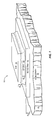
- the placement tool 20 is shown as part of a semiconductor die bonder 22 .
- the placement tool 20 has a head portion for picking and placing the semiconductor die 16 and a shaft extending through a mounting device 24 .
- Ball bearings are provided to enable low-friction movement of the placement tool 20 in relation to the mounting device 24 .
- robotics 28 are provided to enable lateral movement of the die placement system 22 relative to the substrate 12 .
- vertical movement is primarily provided through a reciprocating action of the placement tool 20 relative to the mounting device 24
- the robotics 28 may be configured to move the entire apparatus vertically, including the mounting device 24 and the placement tool 20 .
- the placement tool 20 typically includes a central vacuum chamber 30 extending throughout its length as depicted.
- the vacuum chamber 30 is sufficiently sized to allow a vacuum created in vacuum tubing 32 by vacuum source 34 to move the placement tool 20 up and down, while simultaneously using a portion of the vacuum to pick up and hold the semiconductor die 16 .
- the vacuum chamber 30 is small enough and the vacuum available great enough that the placement tool 20 can be moved up and down without a semiconductor die 16 covering the entrance to the vacuum chamber 30 . Accordingly, the vacuum created in the vacuum chamber 30 is sufficient to pick up and hold the semiconductor die 16 in place during transport.
- the robotics 28 and vacuum source 34 are controlled by a control system 36 having memory 38 with sufficient software and data to control operation of the die bonder 22 .
- the control system 36 will also preferably include a user interface 40 to allow programming, operation, and other control of the die bonder 22 .
- the timed descent for the predefined period of time is preferably triggered by releasing the placement tool 20 to fall toward the bond pad 14 and into epoxy 18 .
- initiation of the timed descent is triggered by instructing the vacuum source 34 to release the vacuum maintained within the vacuum tubing 32 and the vacuum chamber 30 within the placement tool 20 .
- the vacuum when released, decays and allows the placement tool 20 to fall toward the bond pad 14 and into the epoxy 18 in a repeatable fashion.
- the semiconductor die 16 is sufficiently small that surface tension or static electricity will operate to maintain the semiconductor die 16 on the bottom surface of the placement tool 20 from the time the timed descent begins and throughout the time in which the semiconductor die 16 is forced into the epoxy 18 .
- the epoxy 18 will hold the semiconductor die 16 in place as the placement tool 20 is stopped and moved away from the bond pad 14 .
Landscapes
- Engineering & Computer Science (AREA)
- Computer Hardware Design (AREA)
- Microelectronics & Electronic Packaging (AREA)
- Power Engineering (AREA)
- Manufacturing & Machinery (AREA)
- Die Bonding (AREA)
Abstract
Description
Claims (21)
Priority Applications (3)
Application Number | Priority Date | Filing Date | Title |
---|---|---|---|
US09/862,872 US6387733B1 (en) | 2001-05-22 | 2001-05-22 | Time-based semiconductor material attachment |
AU2002305597A AU2002305597A1 (en) | 2001-05-22 | 2002-05-15 | Time-based semiconductor material attachment |
PCT/US2002/015345 WO2002095815A2 (en) | 2001-05-22 | 2002-05-15 | Time-based semiconductor material attachment |
Applications Claiming Priority (1)
Application Number | Priority Date | Filing Date | Title |
---|---|---|---|
US09/862,872 US6387733B1 (en) | 2001-05-22 | 2001-05-22 | Time-based semiconductor material attachment |
Publications (1)
Publication Number | Publication Date |
---|---|
US6387733B1 true US6387733B1 (en) | 2002-05-14 |
Family
ID=25339598
Family Applications (1)
Application Number | Title | Priority Date | Filing Date |
---|---|---|---|
US09/862,872 Expired - Fee Related US6387733B1 (en) | 2001-05-22 | 2001-05-22 | Time-based semiconductor material attachment |
Country Status (3)
Country | Link |
---|---|
US (1) | US6387733B1 (en) |
AU (1) | AU2002305597A1 (en) |
WO (1) | WO2002095815A2 (en) |
Cited By (22)
Publication number | Priority date | Publication date | Assignee | Title |
---|---|---|---|---|
US20040183511A1 (en) * | 2003-03-17 | 2004-09-23 | Rf Micro Devices, Inc. | DC-DC converter with reduced electromagnetic interference |
US20050136640A1 (en) * | 2002-01-07 | 2005-06-23 | Chuan Hu | Die exhibiting an effective coefficient of thermal expansion equivalent to a substrate mounted thereon, and processes of making same |
US20050176209A1 (en) * | 2003-02-14 | 2005-08-11 | Rf Micro Devices, Inc. | Embedded passive components |
US6980039B1 (en) | 2004-03-03 | 2005-12-27 | Rf Micro Devices, Inc. | DC-DC converter with noise spreading to meet spectral mask requirements |
US7033961B1 (en) | 2003-07-15 | 2006-04-25 | Rf Micro Devices, Inc. | Epitaxy/substrate release layer |
US7052942B1 (en) | 2003-09-19 | 2006-05-30 | Rf Micro Devices, Inc. | Surface passivation of GaN devices in epitaxial growth chamber |
US20080153209A1 (en) * | 2002-01-07 | 2008-06-26 | Intel Corporation | Thinned die integrated circuit package |
US8988097B2 (en) | 2012-08-24 | 2015-03-24 | Rf Micro Devices, Inc. | Method for on-wafer high voltage testing of semiconductor devices |
US9070761B2 (en) | 2012-08-27 | 2015-06-30 | Rf Micro Devices, Inc. | Field effect transistor (FET) having fingers with rippled edges |
US9093420B2 (en) | 2012-04-18 | 2015-07-28 | Rf Micro Devices, Inc. | Methods for fabricating high voltage field effect transistor finger terminations |
US9124221B2 (en) | 2012-07-16 | 2015-09-01 | Rf Micro Devices, Inc. | Wide bandwidth radio frequency amplier having dual gate transistors |
US9129802B2 (en) | 2012-08-27 | 2015-09-08 | Rf Micro Devices, Inc. | Lateral semiconductor device with vertical breakdown region |
US9142620B2 (en) | 2012-08-24 | 2015-09-22 | Rf Micro Devices, Inc. | Power device packaging having backmetals couple the plurality of bond pads to the die backside |
US9147632B2 (en) | 2012-08-24 | 2015-09-29 | Rf Micro Devices, Inc. | Semiconductor device having improved heat dissipation |
US9202874B2 (en) | 2012-08-24 | 2015-12-01 | Rf Micro Devices, Inc. | Gallium nitride (GaN) device with leakage current-based over-voltage protection |
US9325281B2 (en) | 2012-10-30 | 2016-04-26 | Rf Micro Devices, Inc. | Power amplifier controller |
US20160148899A1 (en) * | 2013-07-08 | 2016-05-26 | Sony Corporation | Method of determining curing conditions, method of producing circuit device, and circuit device |
US9455327B2 (en) | 2014-06-06 | 2016-09-27 | Qorvo Us, Inc. | Schottky gated transistor with interfacial layer |
US9536803B2 (en) | 2014-09-05 | 2017-01-03 | Qorvo Us, Inc. | Integrated power module with improved isolation and thermal conductivity |
US9917080B2 (en) | 2012-08-24 | 2018-03-13 | Qorvo US. Inc. | Semiconductor device with electrical overstress (EOS) protection |
US10062684B2 (en) | 2015-02-04 | 2018-08-28 | Qorvo Us, Inc. | Transition frequency multiplier semiconductor device |
US10615158B2 (en) | 2015-02-04 | 2020-04-07 | Qorvo Us, Inc. | Transition frequency multiplier semiconductor device |
Citations (22)
Publication number | Priority date | Publication date | Assignee | Title |
---|---|---|---|---|
US4129881A (en) | 1976-03-18 | 1978-12-12 | Ckd Praha, Oborovy Podnik | Heat sink cooled, semiconductor device assembly having liquid metal interface |
US4157273A (en) | 1975-03-20 | 1979-06-05 | Phillips Petroleum Company | Bonding with a poly(arylene sulfide)-polytetrafluoroethylene adhesive |
US4346124A (en) | 1981-05-04 | 1982-08-24 | Laurier Associates, Inc. | Method of applying an adhesive to a circuit chip |
US4545840A (en) | 1983-03-08 | 1985-10-08 | Monolithic Memories, Inc. | Process for controlling thickness of die attach adhesive |
US4749329A (en) | 1982-12-06 | 1988-06-07 | Motorola, Inc. | Die pick mechanism for automatic assembly of semiconductor devices |
US5215608A (en) | 1990-01-24 | 1993-06-01 | Stroud Robert D | Composition and methods for bonding electrical components |
US5336357A (en) | 1993-03-12 | 1994-08-09 | Quantum Materials, Inc. | Manually operable die attach apparatus |
US5765277A (en) | 1995-09-30 | 1998-06-16 | Samsung Electronics Co., Ltd. | Die bonding apparatus with a revolving pick-up tool |
US5882451A (en) | 1996-03-27 | 1999-03-16 | Matsushita Electric Industrial Co., Ltd. | Method and apparatus for applying an electronic component adhesive |
US5994165A (en) | 1997-02-05 | 1999-11-30 | Nec Corporation | Method for mounting a semiconductor chip |
US6037192A (en) | 1998-01-22 | 2000-03-14 | Nortel Networks Corporation | Process of assembling an integrated circuit and a terminal substrate using solder reflow and adhesive cure |
US6051449A (en) | 1997-08-06 | 2000-04-18 | Micron Technology, Inc. | Method and apparatus for Epoxy loc die attachment |
US6077380A (en) | 1995-06-30 | 2000-06-20 | Microfab Technologies, Inc. | Method of forming an adhesive connection |
US6129040A (en) | 1997-09-05 | 2000-10-10 | Esec Sa | Semi-conductor mounting apparatus for applying adhesive to a substrate |
US6135340A (en) | 1997-03-31 | 2000-10-24 | Micron Technology, Inc. | Bonding and inspection system |
US6170736B1 (en) | 1998-05-04 | 2001-01-09 | Motorola, Inc. | Semiconductor die attach method and apparatus therefor |
US6179938B1 (en) | 1997-10-30 | 2001-01-30 | Esec Sa | Method and apparatus for aligning the bonding head of a bonder, in particular a die bonder |
US6206066B1 (en) | 1995-12-15 | 2001-03-27 | Matsushita Electric Industrial Co., Ltd. | Apparatus for mounting an electronic component |
US6309913B1 (en) * | 1996-01-02 | 2001-10-30 | Micron Technology, Inc. | Technique for attaching die to leads |
US6320397B1 (en) * | 1991-06-04 | 2001-11-20 | Micron Technology, Inc. | Molded plastic carrier for testing semiconductor dice |
US6321970B1 (en) * | 1995-12-18 | 2001-11-27 | Micron Technology, Inc. | Wire bonding machine |
US6336974B1 (en) * | 1997-08-05 | 2002-01-08 | Micron Technology, Inc. | Apparatus and method for controlling the depth of immersion of a semiconductor element in an exposed surface of a viscous fluid |
Family Cites Families (4)
Publication number | Priority date | Publication date | Assignee | Title |
---|---|---|---|---|
JP2635889B2 (en) * | 1992-06-24 | 1997-07-30 | 株式会社東芝 | Die bonding equipment |
JP3132496B2 (en) * | 1999-01-25 | 2001-02-05 | 松下電器産業株式会社 | Die bonding equipment |
EP1187181A3 (en) * | 2000-09-12 | 2002-04-10 | Esec Trading S.A. | Method and apparatus for mounting semiconductor chips |
EP1187180A1 (en) * | 2000-09-12 | 2002-03-13 | Esec Trading S.A. | Method and apparatus for mounting semiconductor chips |
-
2001
- 2001-05-22 US US09/862,872 patent/US6387733B1/en not_active Expired - Fee Related
-
2002
- 2002-05-15 WO PCT/US2002/015345 patent/WO2002095815A2/en not_active Application Discontinuation
- 2002-05-15 AU AU2002305597A patent/AU2002305597A1/en not_active Abandoned
Patent Citations (23)
Publication number | Priority date | Publication date | Assignee | Title |
---|---|---|---|---|
US4157273A (en) | 1975-03-20 | 1979-06-05 | Phillips Petroleum Company | Bonding with a poly(arylene sulfide)-polytetrafluoroethylene adhesive |
US4129881A (en) | 1976-03-18 | 1978-12-12 | Ckd Praha, Oborovy Podnik | Heat sink cooled, semiconductor device assembly having liquid metal interface |
US4346124A (en) | 1981-05-04 | 1982-08-24 | Laurier Associates, Inc. | Method of applying an adhesive to a circuit chip |
US4749329A (en) | 1982-12-06 | 1988-06-07 | Motorola, Inc. | Die pick mechanism for automatic assembly of semiconductor devices |
US4545840A (en) | 1983-03-08 | 1985-10-08 | Monolithic Memories, Inc. | Process for controlling thickness of die attach adhesive |
US5215608A (en) | 1990-01-24 | 1993-06-01 | Stroud Robert D | Composition and methods for bonding electrical components |
US6320397B1 (en) * | 1991-06-04 | 2001-11-20 | Micron Technology, Inc. | Molded plastic carrier for testing semiconductor dice |
US5336357A (en) | 1993-03-12 | 1994-08-09 | Quantum Materials, Inc. | Manually operable die attach apparatus |
US6077380A (en) | 1995-06-30 | 2000-06-20 | Microfab Technologies, Inc. | Method of forming an adhesive connection |
US5765277A (en) | 1995-09-30 | 1998-06-16 | Samsung Electronics Co., Ltd. | Die bonding apparatus with a revolving pick-up tool |
US6206066B1 (en) | 1995-12-15 | 2001-03-27 | Matsushita Electric Industrial Co., Ltd. | Apparatus for mounting an electronic component |
US6321970B1 (en) * | 1995-12-18 | 2001-11-27 | Micron Technology, Inc. | Wire bonding machine |
US6309913B1 (en) * | 1996-01-02 | 2001-10-30 | Micron Technology, Inc. | Technique for attaching die to leads |
US5882451A (en) | 1996-03-27 | 1999-03-16 | Matsushita Electric Industrial Co., Ltd. | Method and apparatus for applying an electronic component adhesive |
US5994165A (en) | 1997-02-05 | 1999-11-30 | Nec Corporation | Method for mounting a semiconductor chip |
US6135340A (en) | 1997-03-31 | 2000-10-24 | Micron Technology, Inc. | Bonding and inspection system |
US6336974B1 (en) * | 1997-08-05 | 2002-01-08 | Micron Technology, Inc. | Apparatus and method for controlling the depth of immersion of a semiconductor element in an exposed surface of a viscous fluid |
US6174752B1 (en) | 1997-08-06 | 2001-01-16 | Micron Technology, Inc. | Method and apparatus for epoxy loc die attachment |
US6051449A (en) | 1997-08-06 | 2000-04-18 | Micron Technology, Inc. | Method and apparatus for Epoxy loc die attachment |
US6129040A (en) | 1997-09-05 | 2000-10-10 | Esec Sa | Semi-conductor mounting apparatus for applying adhesive to a substrate |
US6179938B1 (en) | 1997-10-30 | 2001-01-30 | Esec Sa | Method and apparatus for aligning the bonding head of a bonder, in particular a die bonder |
US6037192A (en) | 1998-01-22 | 2000-03-14 | Nortel Networks Corporation | Process of assembling an integrated circuit and a terminal substrate using solder reflow and adhesive cure |
US6170736B1 (en) | 1998-05-04 | 2001-01-09 | Motorola, Inc. | Semiconductor die attach method and apparatus therefor |
Cited By (31)
Publication number | Priority date | Publication date | Assignee | Title |
---|---|---|---|---|
US20080153209A1 (en) * | 2002-01-07 | 2008-06-26 | Intel Corporation | Thinned die integrated circuit package |
US20050136640A1 (en) * | 2002-01-07 | 2005-06-23 | Chuan Hu | Die exhibiting an effective coefficient of thermal expansion equivalent to a substrate mounted thereon, and processes of making same |
US7888183B2 (en) | 2002-01-07 | 2011-02-15 | Intel Corporation | Thinned die integrated circuit package |
US7420273B2 (en) | 2002-01-07 | 2008-09-02 | Intel Corporation | Thinned die integrated circuit package |
US20050176209A1 (en) * | 2003-02-14 | 2005-08-11 | Rf Micro Devices, Inc. | Embedded passive components |
US6969978B2 (en) | 2003-03-17 | 2005-11-29 | Rf Micro Devices, Inc. | DC-DC converter with reduced electromagnetic interference |
US20040183511A1 (en) * | 2003-03-17 | 2004-09-23 | Rf Micro Devices, Inc. | DC-DC converter with reduced electromagnetic interference |
US7033961B1 (en) | 2003-07-15 | 2006-04-25 | Rf Micro Devices, Inc. | Epitaxy/substrate release layer |
US7052942B1 (en) | 2003-09-19 | 2006-05-30 | Rf Micro Devices, Inc. | Surface passivation of GaN devices in epitaxial growth chamber |
US7408182B1 (en) | 2003-09-19 | 2008-08-05 | Rf Micro Devices, Inc. | Surface passivation of GaN devices in epitaxial growth chamber |
US6980039B1 (en) | 2004-03-03 | 2005-12-27 | Rf Micro Devices, Inc. | DC-DC converter with noise spreading to meet spectral mask requirements |
US9564497B2 (en) | 2012-04-18 | 2017-02-07 | Qorvo Us, Inc. | High voltage field effect transitor finger terminations |
US9136341B2 (en) | 2012-04-18 | 2015-09-15 | Rf Micro Devices, Inc. | High voltage field effect transistor finger terminations |
US9093420B2 (en) | 2012-04-18 | 2015-07-28 | Rf Micro Devices, Inc. | Methods for fabricating high voltage field effect transistor finger terminations |
US9124221B2 (en) | 2012-07-16 | 2015-09-01 | Rf Micro Devices, Inc. | Wide bandwidth radio frequency amplier having dual gate transistors |
US8988097B2 (en) | 2012-08-24 | 2015-03-24 | Rf Micro Devices, Inc. | Method for on-wafer high voltage testing of semiconductor devices |
US9142620B2 (en) | 2012-08-24 | 2015-09-22 | Rf Micro Devices, Inc. | Power device packaging having backmetals couple the plurality of bond pads to the die backside |
US9147632B2 (en) | 2012-08-24 | 2015-09-29 | Rf Micro Devices, Inc. | Semiconductor device having improved heat dissipation |
US9202874B2 (en) | 2012-08-24 | 2015-12-01 | Rf Micro Devices, Inc. | Gallium nitride (GaN) device with leakage current-based over-voltage protection |
US9917080B2 (en) | 2012-08-24 | 2018-03-13 | Qorvo US. Inc. | Semiconductor device with electrical overstress (EOS) protection |
US9640632B2 (en) | 2012-08-24 | 2017-05-02 | Qorvo Us, Inc. | Semiconductor device having improved heat dissipation |
US9070761B2 (en) | 2012-08-27 | 2015-06-30 | Rf Micro Devices, Inc. | Field effect transistor (FET) having fingers with rippled edges |
US9129802B2 (en) | 2012-08-27 | 2015-09-08 | Rf Micro Devices, Inc. | Lateral semiconductor device with vertical breakdown region |
US9325281B2 (en) | 2012-10-30 | 2016-04-26 | Rf Micro Devices, Inc. | Power amplifier controller |
US9997491B2 (en) * | 2013-07-08 | 2018-06-12 | Sony Corporation | Method of determining curing conditions, method of producing circuit device, and circuit device |
US20160148899A1 (en) * | 2013-07-08 | 2016-05-26 | Sony Corporation | Method of determining curing conditions, method of producing circuit device, and circuit device |
US10658329B2 (en) | 2013-07-08 | 2020-05-19 | Sony Corporation | Method of determining curing conditions, method of producing circuit device and circuit device |
US9455327B2 (en) | 2014-06-06 | 2016-09-27 | Qorvo Us, Inc. | Schottky gated transistor with interfacial layer |
US9536803B2 (en) | 2014-09-05 | 2017-01-03 | Qorvo Us, Inc. | Integrated power module with improved isolation and thermal conductivity |
US10062684B2 (en) | 2015-02-04 | 2018-08-28 | Qorvo Us, Inc. | Transition frequency multiplier semiconductor device |
US10615158B2 (en) | 2015-02-04 | 2020-04-07 | Qorvo Us, Inc. | Transition frequency multiplier semiconductor device |
Also Published As
Publication number | Publication date |
---|---|
AU2002305597A1 (en) | 2002-12-03 |
WO2002095815A3 (en) | 2003-03-13 |
WO2002095815A2 (en) | 2002-11-28 |
Similar Documents
Publication | Publication Date | Title |
---|---|---|
US6387733B1 (en) | Time-based semiconductor material attachment | |
CN110073478B (en) | Compliant pins for direct delivery of semiconductor devices | |
US5285946A (en) | Apparatus for mounting components | |
US7240822B2 (en) | Ball mounting method | |
US11557567B2 (en) | Methods of attaching die to substrate using compliant die attach system having spring-driven bond tool | |
JPH0613416A (en) | Die bonder | |
TWI270158B (en) | Method and apparatus for the mounting of semiconductor chips | |
US20110315747A1 (en) | Solder ball mounting apparatus, solder ball mounting method, and metal ball mounting apparatus | |
JP3228140B2 (en) | Mounting method of conductive ball | |
JP5191753B2 (en) | Die bonder and die bonding method | |
JP4136692B2 (en) | Pellet conveying device, pellet bonding method and pellet bonding device | |
JPS61234968A (en) | Coating device | |
JP2680773B2 (en) | Pressurizing force control device in component mounting device | |
US6170736B1 (en) | Semiconductor die attach method and apparatus therefor | |
KR0138299Y1 (en) | Die bonding apparatus | |
JP3493984B2 (en) | Transfer method of conductive ball | |
KR20180108178A (en) | Bonding apparatus and method for controlling the same | |
US7407084B2 (en) | Method for mounting a semiconductor chip onto a substrate | |
JP2002118125A (en) | Method and device for mounting semiconductor chip | |
JPH05104349A (en) | Method for controlling impact on component attaching device | |
JP3507704B2 (en) | Method for detecting suction height of micro ball and method for suction of micro ball | |
JPH05337865A (en) | Semiconductor mounting device and mounting method using this device | |
EP1187181A3 (en) | Method and apparatus for mounting semiconductor chips | |
JPH077043A (en) | Inner lead wire bonding device | |
JPS6220337A (en) | Pellet mounting machine |
Legal Events
Date | Code | Title | Description |
---|---|---|---|
AS | Assignment |
Owner name: RF MICRO DEVICES, INC., NORTH CAROLINA Free format text: ASSIGNMENT OF ASSIGNORS INTEREST;ASSIGNORS:HOLYOAK, HOWARD JOSEPH;BAILEY, JOHN CODY;REEL/FRAME:011840/0032 Effective date: 20010518 |
|
AS | Assignment |
Owner name: FIRST UNION NATIONAL BANK, NORTH CAROLINA Free format text: SECURITY INTEREST;ASSIGNOR:RF MICRO DEVICES, INC.;REEL/FRAME:012621/0529 Effective date: 19990813 |
|
AS | Assignment |
Owner name: RF MICRO DEVICES, INC., NORTH CAROLINA Free format text: RELEASE OF SECURITY INTEREST;ASSIGNOR:WACHOVIA BANK, NATIONAL ASSOCIATION, AS ADMINISTRATIVE AGENT;REEL/FRAME:013532/0640 Effective date: 20021119 |
|
REMI | Maintenance fee reminder mailed | ||
LAPS | Lapse for failure to pay maintenance fees | ||
STCH | Information on status: patent discontinuation |
Free format text: PATENT EXPIRED DUE TO NONPAYMENT OF MAINTENANCE FEES UNDER 37 CFR 1.362 |
|
FP | Lapsed due to failure to pay maintenance fee |
Effective date: 20060514 |