US6348159B1 - Method and apparatus for etching coated substrates - Google Patents
Method and apparatus for etching coated substrates Download PDFInfo
- Publication number
- US6348159B1 US6348159B1 US09/250,654 US25065499A US6348159B1 US 6348159 B1 US6348159 B1 US 6348159B1 US 25065499 A US25065499 A US 25065499A US 6348159 B1 US6348159 B1 US 6348159B1
- Authority
- US
- United States
- Prior art keywords
- tank
- etchant
- substrate
- etching
- substrates
- Prior art date
- Legal status (The legal status is an assumption and is not a legal conclusion. Google has not performed a legal analysis and makes no representation as to the accuracy of the status listed.)
- Expired - Lifetime
Links
- 239000000758 substrate Substances 0.000 title claims abstract description 127
- 238000005530 etching Methods 0.000 title claims abstract description 70
- 238000000034 method Methods 0.000 title claims abstract description 58
- 238000000576 coating method Methods 0.000 claims abstract description 137
- 239000011248 coating agent Substances 0.000 claims abstract description 72
- 239000004065 semiconductor Substances 0.000 claims abstract description 28
- 239000000203 mixture Substances 0.000 claims abstract description 19
- XLYOFNOQVPJJNP-UHFFFAOYSA-N water Substances O XLYOFNOQVPJJNP-UHFFFAOYSA-N 0.000 claims description 32
- 239000012530 fluid Substances 0.000 claims description 30
- MARUHZGHZWCEQU-UHFFFAOYSA-N 5-phenyl-2h-tetrazole Chemical compound C1=CC=CC=C1C1=NNN=N1 MARUHZGHZWCEQU-UHFFFAOYSA-N 0.000 claims description 28
- 239000011521 glass Substances 0.000 claims description 17
- XOLBLPGZBRYERU-UHFFFAOYSA-N tin dioxide Chemical compound O=[Sn]=O XOLBLPGZBRYERU-UHFFFAOYSA-N 0.000 claims description 17
- 229910001887 tin oxide Inorganic materials 0.000 claims description 14
- 239000000463 material Substances 0.000 claims description 13
- BDOSMKKIYDKNTQ-UHFFFAOYSA-N cadmium atom Chemical compound [Cd] BDOSMKKIYDKNTQ-UHFFFAOYSA-N 0.000 claims description 12
- 229910052793 cadmium Inorganic materials 0.000 claims description 11
- QAOWNCQODCNURD-UHFFFAOYSA-N Sulfuric acid Chemical compound OS(O)(=O)=O QAOWNCQODCNURD-UHFFFAOYSA-N 0.000 claims description 8
- 239000003929 acidic solution Substances 0.000 claims description 4
- 238000007599 discharging Methods 0.000 claims description 3
- 229920006395 saturated elastomer Polymers 0.000 claims 2
- 239000000243 solution Substances 0.000 claims 2
- 238000005507 spraying Methods 0.000 claims 2
- 238000004891 communication Methods 0.000 description 25
- 238000005086 pumping Methods 0.000 description 19
- WUPHOULIZUERAE-UHFFFAOYSA-N 3-(oxolan-2-yl)propanoic acid Chemical compound OC(=O)CCC1CCCO1 WUPHOULIZUERAE-UHFFFAOYSA-N 0.000 description 15
- 229910052980 cadmium sulfide Inorganic materials 0.000 description 15
- 239000010410 layer Substances 0.000 description 14
- 239000007921 spray Substances 0.000 description 7
- 229910052751 metal Inorganic materials 0.000 description 6
- 239000002184 metal Substances 0.000 description 6
- 230000002950 deficient Effects 0.000 description 5
- 238000000151 deposition Methods 0.000 description 4
- 229910052714 tellurium Inorganic materials 0.000 description 3
- PORWMNRCUJJQNO-UHFFFAOYSA-N tellurium atom Chemical compound [Te] PORWMNRCUJJQNO-UHFFFAOYSA-N 0.000 description 3
- VEXZGXHMUGYJMC-UHFFFAOYSA-N Hydrochloric acid Chemical compound Cl VEXZGXHMUGYJMC-UHFFFAOYSA-N 0.000 description 2
- MHAJPDPJQMAIIY-UHFFFAOYSA-N Hydrogen peroxide Chemical compound OO MHAJPDPJQMAIIY-UHFFFAOYSA-N 0.000 description 2
- NINIDFKCEFEMDL-UHFFFAOYSA-N Sulfur Chemical compound [S] NINIDFKCEFEMDL-UHFFFAOYSA-N 0.000 description 2
- 230000003213 activating effect Effects 0.000 description 2
- 239000008367 deionised water Substances 0.000 description 2
- 230000008021 deposition Effects 0.000 description 2
- 239000005038 ethylene vinyl acetate Substances 0.000 description 2
- 150000002739 metals Chemical class 0.000 description 2
- -1 polyethylene Polymers 0.000 description 2
- PXGOKWXKJXAPGV-UHFFFAOYSA-N Fluorine Chemical compound FF PXGOKWXKJXAPGV-UHFFFAOYSA-N 0.000 description 1
- DGAQECJNVWCQMB-PUAWFVPOSA-M Ilexoside XXIX Chemical compound C[C@@H]1CC[C@@]2(CC[C@@]3(C(=CC[C@H]4[C@]3(CC[C@@H]5[C@@]4(CC[C@@H](C5(C)C)OS(=O)(=O)[O-])C)C)[C@@H]2[C@]1(C)O)C)C(=O)O[C@H]6[C@@H]([C@H]([C@@H]([C@H](O6)CO)O)O)O.[Na+] DGAQECJNVWCQMB-PUAWFVPOSA-M 0.000 description 1
- 229910021578 Iron(III) chloride Inorganic materials 0.000 description 1
- GRYLNZFGIOXLOG-UHFFFAOYSA-N Nitric acid Chemical compound O[N+]([O-])=O GRYLNZFGIOXLOG-UHFFFAOYSA-N 0.000 description 1
- 239000004698 Polyethylene Substances 0.000 description 1
- 239000004743 Polypropylene Substances 0.000 description 1
- BUGBHKTXTAQXES-UHFFFAOYSA-N Selenium Chemical compound [Se] BUGBHKTXTAQXES-UHFFFAOYSA-N 0.000 description 1
- BQCADISMDOOEFD-UHFFFAOYSA-N Silver Chemical compound [Ag] BQCADISMDOOEFD-UHFFFAOYSA-N 0.000 description 1
- QAOWNCQODCNURD-UHFFFAOYSA-L Sulfate Chemical compound [O-]S([O-])(=O)=O QAOWNCQODCNURD-UHFFFAOYSA-L 0.000 description 1
- 229920006362 Teflon® Polymers 0.000 description 1
- 239000002253 acid Substances 0.000 description 1
- 150000007513 acids Chemical class 0.000 description 1
- 239000003945 anionic surfactant Substances 0.000 description 1
- 229910052788 barium Inorganic materials 0.000 description 1
- DSAJWYNOEDNPEQ-UHFFFAOYSA-N barium atom Chemical compound [Ba] DSAJWYNOEDNPEQ-UHFFFAOYSA-N 0.000 description 1
- 229940065285 cadmium compound Drugs 0.000 description 1
- 150000001662 cadmium compounds Chemical class 0.000 description 1
- 239000004020 conductor Substances 0.000 description 1
- HVMJUDPAXRRVQO-UHFFFAOYSA-N copper indium Chemical compound [Cu].[In] HVMJUDPAXRRVQO-UHFFFAOYSA-N 0.000 description 1
- 229910021641 deionized water Inorganic materials 0.000 description 1
- 238000005137 deposition process Methods 0.000 description 1
- 238000005516 engineering process Methods 0.000 description 1
- 229910052731 fluorine Inorganic materials 0.000 description 1
- 239000011737 fluorine Substances 0.000 description 1
- PCHJSUWPFVWCPO-UHFFFAOYSA-N gold Chemical compound [Au] PCHJSUWPFVWCPO-UHFFFAOYSA-N 0.000 description 1
- 229910052737 gold Inorganic materials 0.000 description 1
- 239000010931 gold Substances 0.000 description 1
- 239000002198 insoluble material Substances 0.000 description 1
- RBTARNINKXHZNM-UHFFFAOYSA-K iron trichloride Chemical compound Cl[Fe](Cl)Cl RBTARNINKXHZNM-UHFFFAOYSA-K 0.000 description 1
- 238000004519 manufacturing process Methods 0.000 description 1
- QSHDDOUJBYECFT-UHFFFAOYSA-N mercury Chemical compound [Hg] QSHDDOUJBYECFT-UHFFFAOYSA-N 0.000 description 1
- 229910052753 mercury Inorganic materials 0.000 description 1
- 239000003595 mist Substances 0.000 description 1
- SNICXCGAKADSCV-UHFFFAOYSA-N nicotine Chemical compound CN1CCCC1C1=CC=CN=C1 SNICXCGAKADSCV-UHFFFAOYSA-N 0.000 description 1
- 229910017604 nitric acid Inorganic materials 0.000 description 1
- 230000009972 noncorrosive effect Effects 0.000 description 1
- 239000002245 particle Substances 0.000 description 1
- 239000004033 plastic Substances 0.000 description 1
- 229920003023 plastic Polymers 0.000 description 1
- 229920000573 polyethylene Polymers 0.000 description 1
- 239000013047 polymeric layer Substances 0.000 description 1
- 229920001155 polypropylene Polymers 0.000 description 1
- 239000010453 quartz Substances 0.000 description 1
- 230000000717 retained effect Effects 0.000 description 1
- 229910052711 selenium Inorganic materials 0.000 description 1
- 239000011669 selenium Substances 0.000 description 1
- VYPSYNLAJGMNEJ-UHFFFAOYSA-N silicon dioxide Inorganic materials O=[Si]=O VYPSYNLAJGMNEJ-UHFFFAOYSA-N 0.000 description 1
- 229910052709 silver Inorganic materials 0.000 description 1
- 239000004332 silver Substances 0.000 description 1
- 229910052708 sodium Inorganic materials 0.000 description 1
- 239000011734 sodium Substances 0.000 description 1
- 150000003498 tellurium compounds Chemical class 0.000 description 1
- 239000002023 wood Substances 0.000 description 1
Images


Classifications
-
- H—ELECTRICITY
- H01—ELECTRIC ELEMENTS
- H01L—SEMICONDUCTOR DEVICES NOT COVERED BY CLASS H10
- H01L21/00—Processes or apparatus adapted for the manufacture or treatment of semiconductor or solid state devices or of parts thereof
- H01L21/67—Apparatus specially adapted for handling semiconductor or electric solid state devices during manufacture or treatment thereof; Apparatus specially adapted for handling wafers during manufacture or treatment of semiconductor or electric solid state devices or components ; Apparatus not specifically provided for elsewhere
- H01L21/67005—Apparatus not specifically provided for elsewhere
- H01L21/67011—Apparatus for manufacture or treatment
- H01L21/67017—Apparatus for fluid treatment
- H01L21/67063—Apparatus for fluid treatment for etching
- H01L21/67075—Apparatus for fluid treatment for etching for wet etching
- H01L21/67086—Apparatus for fluid treatment for etching for wet etching with the semiconductor substrates being dipped in baths or vessels
-
- C—CHEMISTRY; METALLURGY
- C03—GLASS; MINERAL OR SLAG WOOL
- C03C—CHEMICAL COMPOSITION OF GLASSES, GLAZES OR VITREOUS ENAMELS; SURFACE TREATMENT OF GLASS; SURFACE TREATMENT OF FIBRES OR FILAMENTS MADE FROM GLASS, MINERALS OR SLAGS; JOINING GLASS TO GLASS OR OTHER MATERIALS
- C03C15/00—Surface treatment of glass, not in the form of fibres or filaments, by etching
-
- C—CHEMISTRY; METALLURGY
- C03—GLASS; MINERAL OR SLAG WOOL
- C03C—CHEMICAL COMPOSITION OF GLASSES, GLAZES OR VITREOUS ENAMELS; SURFACE TREATMENT OF GLASS; SURFACE TREATMENT OF FIBRES OR FILAMENTS MADE FROM GLASS, MINERALS OR SLAGS; JOINING GLASS TO GLASS OR OTHER MATERIALS
- C03C17/00—Surface treatment of glass, not in the form of fibres or filaments, by coating
- C03C17/06—Surface treatment of glass, not in the form of fibres or filaments, by coating with metals
-
- C—CHEMISTRY; METALLURGY
- C03—GLASS; MINERAL OR SLAG WOOL
- C03C—CHEMICAL COMPOSITION OF GLASSES, GLAZES OR VITREOUS ENAMELS; SURFACE TREATMENT OF GLASS; SURFACE TREATMENT OF FIBRES OR FILAMENTS MADE FROM GLASS, MINERALS OR SLAGS; JOINING GLASS TO GLASS OR OTHER MATERIALS
- C03C17/00—Surface treatment of glass, not in the form of fibres or filaments, by coating
- C03C17/22—Surface treatment of glass, not in the form of fibres or filaments, by coating with other inorganic material
-
- C—CHEMISTRY; METALLURGY
- C03—GLASS; MINERAL OR SLAG WOOL
- C03C—CHEMICAL COMPOSITION OF GLASSES, GLAZES OR VITREOUS ENAMELS; SURFACE TREATMENT OF GLASS; SURFACE TREATMENT OF FIBRES OR FILAMENTS MADE FROM GLASS, MINERALS OR SLAGS; JOINING GLASS TO GLASS OR OTHER MATERIALS
- C03C17/00—Surface treatment of glass, not in the form of fibres or filaments, by coating
- C03C17/34—Surface treatment of glass, not in the form of fibres or filaments, by coating with at least two coatings having different compositions
-
- C—CHEMISTRY; METALLURGY
- C23—COATING METALLIC MATERIAL; COATING MATERIAL WITH METALLIC MATERIAL; CHEMICAL SURFACE TREATMENT; DIFFUSION TREATMENT OF METALLIC MATERIAL; COATING BY VACUUM EVAPORATION, BY SPUTTERING, BY ION IMPLANTATION OR BY CHEMICAL VAPOUR DEPOSITION, IN GENERAL; INHIBITING CORROSION OF METALLIC MATERIAL OR INCRUSTATION IN GENERAL
- C23F—NON-MECHANICAL REMOVAL OF METALLIC MATERIAL FROM SURFACE; INHIBITING CORROSION OF METALLIC MATERIAL OR INCRUSTATION IN GENERAL; MULTI-STEP PROCESSES FOR SURFACE TREATMENT OF METALLIC MATERIAL INVOLVING AT LEAST ONE PROCESS PROVIDED FOR IN CLASS C23 AND AT LEAST ONE PROCESS COVERED BY SUBCLASS C21D OR C22F OR CLASS C25
- C23F1/00—Etching metallic material by chemical means
- C23F1/08—Apparatus, e.g. for photomechanical printing surfaces
-
- H—ELECTRICITY
- H01—ELECTRIC ELEMENTS
- H01L—SEMICONDUCTOR DEVICES NOT COVERED BY CLASS H10
- H01L31/00—Semiconductor devices sensitive to infrared radiation, light, electromagnetic radiation of shorter wavelength or corpuscular radiation and specially adapted either for the conversion of the energy of such radiation into electrical energy or for the control of electrical energy by such radiation; Processes or apparatus specially adapted for the manufacture or treatment thereof or of parts thereof; Details thereof
- H01L31/0248—Semiconductor devices sensitive to infrared radiation, light, electromagnetic radiation of shorter wavelength or corpuscular radiation and specially adapted either for the conversion of the energy of such radiation into electrical energy or for the control of electrical energy by such radiation; Processes or apparatus specially adapted for the manufacture or treatment thereof or of parts thereof; Details thereof characterised by their semiconductor bodies
- H01L31/036—Semiconductor devices sensitive to infrared radiation, light, electromagnetic radiation of shorter wavelength or corpuscular radiation and specially adapted either for the conversion of the energy of such radiation into electrical energy or for the control of electrical energy by such radiation; Processes or apparatus specially adapted for the manufacture or treatment thereof or of parts thereof; Details thereof characterised by their semiconductor bodies characterised by their crystalline structure or particular orientation of the crystalline planes
- H01L31/0392—Semiconductor devices sensitive to infrared radiation, light, electromagnetic radiation of shorter wavelength or corpuscular radiation and specially adapted either for the conversion of the energy of such radiation into electrical energy or for the control of electrical energy by such radiation; Processes or apparatus specially adapted for the manufacture or treatment thereof or of parts thereof; Details thereof characterised by their semiconductor bodies characterised by their crystalline structure or particular orientation of the crystalline planes including thin films deposited on metallic or insulating substrates ; characterised by specific substrate materials or substrate features or by the presence of intermediate layers, e.g. barrier layers, on the substrate
- H01L31/03923—Semiconductor devices sensitive to infrared radiation, light, electromagnetic radiation of shorter wavelength or corpuscular radiation and specially adapted either for the conversion of the energy of such radiation into electrical energy or for the control of electrical energy by such radiation; Processes or apparatus specially adapted for the manufacture or treatment thereof or of parts thereof; Details thereof characterised by their semiconductor bodies characterised by their crystalline structure or particular orientation of the crystalline planes including thin films deposited on metallic or insulating substrates ; characterised by specific substrate materials or substrate features or by the presence of intermediate layers, e.g. barrier layers, on the substrate including AIBIIICVI compound materials, e.g. CIS, CIGS
-
- H—ELECTRICITY
- H01—ELECTRIC ELEMENTS
- H01L—SEMICONDUCTOR DEVICES NOT COVERED BY CLASS H10
- H01L31/00—Semiconductor devices sensitive to infrared radiation, light, electromagnetic radiation of shorter wavelength or corpuscular radiation and specially adapted either for the conversion of the energy of such radiation into electrical energy or for the control of electrical energy by such radiation; Processes or apparatus specially adapted for the manufacture or treatment thereof or of parts thereof; Details thereof
- H01L31/0248—Semiconductor devices sensitive to infrared radiation, light, electromagnetic radiation of shorter wavelength or corpuscular radiation and specially adapted either for the conversion of the energy of such radiation into electrical energy or for the control of electrical energy by such radiation; Processes or apparatus specially adapted for the manufacture or treatment thereof or of parts thereof; Details thereof characterised by their semiconductor bodies
- H01L31/036—Semiconductor devices sensitive to infrared radiation, light, electromagnetic radiation of shorter wavelength or corpuscular radiation and specially adapted either for the conversion of the energy of such radiation into electrical energy or for the control of electrical energy by such radiation; Processes or apparatus specially adapted for the manufacture or treatment thereof or of parts thereof; Details thereof characterised by their semiconductor bodies characterised by their crystalline structure or particular orientation of the crystalline planes
- H01L31/0392—Semiconductor devices sensitive to infrared radiation, light, electromagnetic radiation of shorter wavelength or corpuscular radiation and specially adapted either for the conversion of the energy of such radiation into electrical energy or for the control of electrical energy by such radiation; Processes or apparatus specially adapted for the manufacture or treatment thereof or of parts thereof; Details thereof characterised by their semiconductor bodies characterised by their crystalline structure or particular orientation of the crystalline planes including thin films deposited on metallic or insulating substrates ; characterised by specific substrate materials or substrate features or by the presence of intermediate layers, e.g. barrier layers, on the substrate
- H01L31/03925—Semiconductor devices sensitive to infrared radiation, light, electromagnetic radiation of shorter wavelength or corpuscular radiation and specially adapted either for the conversion of the energy of such radiation into electrical energy or for the control of electrical energy by such radiation; Processes or apparatus specially adapted for the manufacture or treatment thereof or of parts thereof; Details thereof characterised by their semiconductor bodies characterised by their crystalline structure or particular orientation of the crystalline planes including thin films deposited on metallic or insulating substrates ; characterised by specific substrate materials or substrate features or by the presence of intermediate layers, e.g. barrier layers, on the substrate including AIIBVI compound materials, e.g. CdTe, CdS
-
- H—ELECTRICITY
- H01—ELECTRIC ELEMENTS
- H01L—SEMICONDUCTOR DEVICES NOT COVERED BY CLASS H10
- H01L31/00—Semiconductor devices sensitive to infrared radiation, light, electromagnetic radiation of shorter wavelength or corpuscular radiation and specially adapted either for the conversion of the energy of such radiation into electrical energy or for the control of electrical energy by such radiation; Processes or apparatus specially adapted for the manufacture or treatment thereof or of parts thereof; Details thereof
- H01L31/18—Processes or apparatus specially adapted for the manufacture or treatment of these devices or of parts thereof
- H01L31/1828—Processes or apparatus specially adapted for the manufacture or treatment of these devices or of parts thereof the active layers comprising only AIIBVI compounds, e.g. CdS, ZnS, CdTe
-
- C—CHEMISTRY; METALLURGY
- C03—GLASS; MINERAL OR SLAG WOOL
- C03C—CHEMICAL COMPOSITION OF GLASSES, GLAZES OR VITREOUS ENAMELS; SURFACE TREATMENT OF GLASS; SURFACE TREATMENT OF FIBRES OR FILAMENTS MADE FROM GLASS, MINERALS OR SLAGS; JOINING GLASS TO GLASS OR OTHER MATERIALS
- C03C2218/00—Methods for coating glass
- C03C2218/30—Aspects of methods for coating glass not covered above
- C03C2218/32—After-treatment
- C03C2218/328—Partly or completely removing a coating
- C03C2218/33—Partly or completely removing a coating by etching
-
- H—ELECTRICITY
- H01—ELECTRIC ELEMENTS
- H01L—SEMICONDUCTOR DEVICES NOT COVERED BY CLASS H10
- H01L21/00—Processes or apparatus adapted for the manufacture or treatment of semiconductor or solid state devices or of parts thereof
- H01L21/02—Manufacture or treatment of semiconductor devices or of parts thereof
- H01L21/04—Manufacture or treatment of semiconductor devices or of parts thereof the devices having at least one potential-jump barrier or surface barrier, e.g. PN junction, depletion layer or carrier concentration layer
- H01L21/18—Manufacture or treatment of semiconductor devices or of parts thereof the devices having at least one potential-jump barrier or surface barrier, e.g. PN junction, depletion layer or carrier concentration layer the devices having semiconductor bodies comprising elements of Group IV of the Periodic System or AIIIBV compounds with or without impurities, e.g. doping materials
- H01L21/30—Treatment of semiconductor bodies using processes or apparatus not provided for in groups H01L21/20 - H01L21/26
- H01L21/302—Treatment of semiconductor bodies using processes or apparatus not provided for in groups H01L21/20 - H01L21/26 to change their surface-physical characteristics or shape, e.g. etching, polishing, cutting
- H01L21/306—Chemical or electrical treatment, e.g. electrolytic etching
- H01L21/30604—Chemical etching
-
- H—ELECTRICITY
- H01—ELECTRIC ELEMENTS
- H01L—SEMICONDUCTOR DEVICES NOT COVERED BY CLASS H10
- H01L21/00—Processes or apparatus adapted for the manufacture or treatment of semiconductor or solid state devices or of parts thereof
- H01L21/02—Manufacture or treatment of semiconductor devices or of parts thereof
- H01L21/04—Manufacture or treatment of semiconductor devices or of parts thereof the devices having at least one potential-jump barrier or surface barrier, e.g. PN junction, depletion layer or carrier concentration layer
- H01L21/18—Manufacture or treatment of semiconductor devices or of parts thereof the devices having at least one potential-jump barrier or surface barrier, e.g. PN junction, depletion layer or carrier concentration layer the devices having semiconductor bodies comprising elements of Group IV of the Periodic System or AIIIBV compounds with or without impurities, e.g. doping materials
- H01L21/30—Treatment of semiconductor bodies using processes or apparatus not provided for in groups H01L21/20 - H01L21/26
- H01L21/31—Treatment of semiconductor bodies using processes or apparatus not provided for in groups H01L21/20 - H01L21/26 to form insulating layers thereon, e.g. for masking or by using photolithographic techniques; After treatment of these layers; Selection of materials for these layers
- H01L21/3105—After-treatment
- H01L21/311—Etching the insulating layers by chemical or physical means
- H01L21/31105—Etching inorganic layers
- H01L21/31111—Etching inorganic layers by chemical means
-
- H—ELECTRICITY
- H01—ELECTRIC ELEMENTS
- H01L—SEMICONDUCTOR DEVICES NOT COVERED BY CLASS H10
- H01L21/00—Processes or apparatus adapted for the manufacture or treatment of semiconductor or solid state devices or of parts thereof
- H01L21/02—Manufacture or treatment of semiconductor devices or of parts thereof
- H01L21/04—Manufacture or treatment of semiconductor devices or of parts thereof the devices having at least one potential-jump barrier or surface barrier, e.g. PN junction, depletion layer or carrier concentration layer
- H01L21/18—Manufacture or treatment of semiconductor devices or of parts thereof the devices having at least one potential-jump barrier or surface barrier, e.g. PN junction, depletion layer or carrier concentration layer the devices having semiconductor bodies comprising elements of Group IV of the Periodic System or AIIIBV compounds with or without impurities, e.g. doping materials
- H01L21/30—Treatment of semiconductor bodies using processes or apparatus not provided for in groups H01L21/20 - H01L21/26
- H01L21/31—Treatment of semiconductor bodies using processes or apparatus not provided for in groups H01L21/20 - H01L21/26 to form insulating layers thereon, e.g. for masking or by using photolithographic techniques; After treatment of these layers; Selection of materials for these layers
- H01L21/3205—Deposition of non-insulating-, e.g. conductive- or resistive-, layers on insulating layers; After-treatment of these layers
- H01L21/321—After treatment
- H01L21/3213—Physical or chemical etching of the layers, e.g. to produce a patterned layer from a pre-deposited extensive layer
- H01L21/32133—Physical or chemical etching of the layers, e.g. to produce a patterned layer from a pre-deposited extensive layer by chemical means only
- H01L21/32134—Physical or chemical etching of the layers, e.g. to produce a patterned layer from a pre-deposited extensive layer by chemical means only by liquid etching only
-
- Y—GENERAL TAGGING OF NEW TECHNOLOGICAL DEVELOPMENTS; GENERAL TAGGING OF CROSS-SECTIONAL TECHNOLOGIES SPANNING OVER SEVERAL SECTIONS OF THE IPC; TECHNICAL SUBJECTS COVERED BY FORMER USPC CROSS-REFERENCE ART COLLECTIONS [XRACs] AND DIGESTS
- Y02—TECHNOLOGIES OR APPLICATIONS FOR MITIGATION OR ADAPTATION AGAINST CLIMATE CHANGE
- Y02E—REDUCTION OF GREENHOUSE GAS [GHG] EMISSIONS, RELATED TO ENERGY GENERATION, TRANSMISSION OR DISTRIBUTION
- Y02E10/00—Energy generation through renewable energy sources
- Y02E10/50—Photovoltaic [PV] energy
- Y02E10/541—CuInSe2 material PV cells
-
- Y—GENERAL TAGGING OF NEW TECHNOLOGICAL DEVELOPMENTS; GENERAL TAGGING OF CROSS-SECTIONAL TECHNOLOGIES SPANNING OVER SEVERAL SECTIONS OF THE IPC; TECHNICAL SUBJECTS COVERED BY FORMER USPC CROSS-REFERENCE ART COLLECTIONS [XRACs] AND DIGESTS
- Y02—TECHNOLOGIES OR APPLICATIONS FOR MITIGATION OR ADAPTATION AGAINST CLIMATE CHANGE
- Y02E—REDUCTION OF GREENHOUSE GAS [GHG] EMISSIONS, RELATED TO ENERGY GENERATION, TRANSMISSION OR DISTRIBUTION
- Y02E10/00—Energy generation through renewable energy sources
- Y02E10/50—Photovoltaic [PV] energy
- Y02E10/543—Solar cells from Group II-VI materials
Definitions
- This invention relates to a method and apparatus for etching substrates having a coating selected from the group consisting of semiconductor coatings, metallic coatings, and mixtures thereof.
- CdTe PV solar cell modules are typically made by providing a base substrate comprising a first glass layer having a coating of tin oxide (SnO 2 ) deposited thereon, depositing a coating of semiconductor cadmium sulfide (CdS) over the tin oxide coating, then depositing a coating of semiconductor cadmium telluride (CdTe) over the cadmium sulfide coating, then adhering a metal contact layer onto the cadmium telluride coating, then adhering a layer of polymeric material, such as ethylene-vinyl acetate (EVA), onto the metal contact layer, followed by adhering a second glass layer onto the polymeric layer.
- a base substrate comprising a first glass layer having a coating of tin oxide (SnO 2 ) deposited thereon, depositing a coating of semiconductor cadmium sulfide (CdS) over the tin oxide coating, then depositing a coating of semiconductor cadmium telluri
- Each coating or layer is built up onto the underlying coating or layer in successive steps. After each coating is deposited, the coating is analyzed to ensure that the coating has been properly deposited. Any solar cell module formed with defective coatings would itself be defective. Processing errors in the deposition of the cadmium sulfide coating or the cadmium telluride coating occur with relative frequency, such as on the order of about 10% of the time. Examples of processing errors include, but are not limited to, improper coating thickness and insufficient coating uniformity.
- substrates which have been improperly coated are often discarded, rather than recycled, because there has not been an inexpensive, convenient, and easy method for removing the improperly deposited coatings while leaving the substrate intact. It would be desirable to provide an inexpensive method for removing improperly deposited conductive coatings without damaging the base substrate intact.
- One object of the present invention is to provide an inexpensive method for removing coatings from substrates having a coating selected from the group consisting of semiconductor coatings, metallic coatings, and mixtures thereof while keeping the substrate intact.
- Another object of the present invention is to provide an apparatus having a small footprint which is capable of removing coatings from substrates having a coating selected from the group consisting of semiconductor coatings, metallic coatings, and mixtures thereof while keeping the substrate intact.
- Yet another object of the present invention is to provide an inexpensive method for removing defective cadmium coatings from cadmium telluride photovoltaic solar cell module subassemblies while leaving the glass substrate intact with the tin oxide coating adhered thereto.
- Still yet another object of the present invention is to provide an apparatus having a relatively small footprint which is capable of removing defective cadmium coatings from cadmium telluride photovoltaic solar cell module subassemblies while leaving the glass substrate intact with the tin oxide coating adhered thereto.
- the present invention provides a method for etching substrates having a coating selected from the group consisting of semiconductor coatings, metallic coatings, and mixtures thereof.
- the method comprises providing at least a first and a second substrate having a coating selected from the group consisting of semiconductor coatings, metallic coatings, and mixtures thereof and introducing at least the first substrate and an etchant into a first tank to etch at least a portion of the coating from the substrate.
- At least the second substrate is introduced into a second tank and the etchant is transferred from the first tank to the second tank to etch at least a portion of the coating from the second substrate.
- the etched first substrate is then removed from the first tank.
- the present invention also provides an apparatus for etching substrates having a coating selected from the group consisting of semiconductor coatings, metallic coatings, and mixtures thereof.
- the apparatus comprises a first tank for receiving a substrate having a coating selected from the group consisting of semiconductor coatings, metallic coatings and mixtures thereof.
- the apparatus also includes a second tank for receiving an etchant, and a pump for pumping the etchant from the second tank to the first tank to etch at least a portion of the coating from the substrate and for thereafter pumping the etchant back to the first tank.
- the present invention further provides a method for etching a substrate having a coating selected from the group consisting of semiconductor coatings, metallic coatings, and mixtures thereof.
- the method comprises introducing the substrate into a first tank.
- An etchant capable of etching the coating from the substrate is introduced into a second tank.
- the etchant is transferred from the second tank to the first tank to provide etching of at least a portion of the coating from the substrate within the first tank.
- the etchant is transferred from the first tank back to the second tank, and the etched substrate is then removed from the first tank.
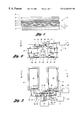
- FIG. 1 is a sectional view of a cadmium telluride photovoltaic solar cell module
- FIG. 2 is an elevational view of an apparatus for use with the method of the present invention
- FIG. 3 is a view taken along line 3 — 3 of FIG. 2;
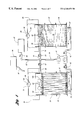
- FIG. 4 is a view taken along line 4 — 4 of FIG. 3 and shown one stage of the method of the present invention
- FIG. 5 is a view similar to FIG. 4 and shows a different stage of the method of the present invention
- FIG. 6 is a view similar to FIG. 5 showing a different stage of the method of the present invention.
- FIG. 7 is a view similar to FIG. 6 showing a differing stage of the method of the present invention.
- FIG. 8 is a view similar to FIG. 7 showing a different stage of the method of the present invention.
- FIG. 9 is a perspective view of an apparatus for use with the present invention.
- the present invention relates to a method for etching, i.e., removing, coatings from at least one substrate having a coating selected from the group consisting of semiconductor coatings, metallic coatings, and mixtures thereof, while keeping the substrate intact.
- the method may vary in dependence upon the article, and in particular, upon the materials which comprise the article.
- the present invention also relates to an apparatus for performing the method of the present invention. The method and the apparatus of the present invention will be described hereinafter in an integrated manner to help facilitate an understanding of the different aspects of the present invention.
- Examples of materials which the substrate may be made of include, but are not limited to, glass, wood and plastic.
- Coatings for which the present invention is useable with are etchable metallic coatings, semiconductor coatings, and mixtures thereof.
- Examples of etchable coatings for which the present invention is useable with include coatings made of, but not limited to, barium, cadmium, lead, mercury, selenium, silver, tellurium, and gold.
- Examples of substrates coated with at least one coating selected from the group consisting of semiconductor coatings, metallic coatings, and mixtures thereof include, but are not limited to, copper indium diselinide photovoltaic solar cell modules, glass mirrors, and plasma flat panel displays.
- the present invention is particularly well suited for removing off-specification semiconductor cadmium coatings from cadmium telluride photovoltaic solar cell module subassemblies, and as such, will be described herein in connection with them, but in doing so is not intended to limit its applicability to just cadmium telluride photovoltaic solar cell module subassemblies.
- the module 10 comprises a first glass substrate 12 .
- the glass substrate 12 has a coating of tin oxide (SnO 2 ) 14 , which is preferably doped with fluorine (SnO 2 :F), adhered thereto and overlying the glass substrate 12 .
- the glass substrate 12 and the tin oxide coating 14 can be provided as a unitary, preformed base substrate 16 from a suitable supplier.
- a semiconductor cadmium sulfide (CdS) coating 18 is adhered to and overlies the tin oxide coating 14 .
- the cadmium sulfide coating 18 is preferably deposited over the tin oxide layer 14 in any suitable manner known in the art.
- a semiconductor cadmium telluride (CdTe) coating 20 is adhered to and overlies the cadmium sulfide coating 18 .
- the cadmium telluride coating 20 is preferably deposited on the cadmium sulfide coating 18 in any suitable manner known in the art.
- the glass substrate 12 , the tin oxide coating 14 , the cadmium sulfide coating 18 and the cadmium telluride coating 20 together form a cadmium telluride photovoltaic solar cell module subassembly 22 .
- a metal contact layer 24 is adhered to and overlies the subassembly 22 , i.e, the cadmium telluride coating 20 .
- a layer of polymeric material 26 preferably ethylene-vinyl acetate (EVA), is adhered to and overlies the metal contact layer 24 .
- EVA ethylene-vinyl acetate
- a second glass substrate 28 is adhered to and overlies the layer of polymeric material 26 .
- the method of the present invention is useful, when it is desirable to remove the cadmium sulfide coating 18 , the cadmium telluride coating 20 , or both, when off-specification coatings have been deposited on the base substrate 16 .
- an etching apparatus 30 which is useable with the method of the present invention, is shown.
- the etching apparatus 30 comprises a first tank 32 and a second tank 34 .
- Each tank 32 and 34 is preferably a tank formed of a non-corrosive material such as polyethylene or polypropylene.
- Each tank 32 and 34 has a chamber 36 and 38 , respectively, which is defined by a base member and a sidewall member extending axially from the base member.
- the etching apparatus 30 also includes a pumping device 42 for transferring fluid, and more particularly an etchant, between the chamber 36 and 38 , and between each chamber 36 , 38 and a reclamation device 43 , as will be explained further below.
- the pumping device 42 is preferably a diaphragm pump, such as a Warren Rupp 1′′ Diaphragm Pump.
- the etchant apparatus 30 also includes a first conduit 44 which extends between, and provides fluid communication between, the first tank 32 and a three-way junction 45 (FIG. 3 ).
- the first conduit 44 has a first end which extends through the base member of the first tank 32 , and a second end which communicates with the three-way junction 45 .
- the three-way junction 45 also communicates with a second conduit 46 .
- the first conduit 44 and the three-way junction 45 thus, extend between, and provide fluid communication between, the first tank 32 and the second conduit 46 .
- the first conduit 44 has a first valve device 48 disposed between the first tank 32 and the second conduit 46 .
- the first valve device 48 has an open condition wherein fluid communication is established between the first tank 32 and the second conduit 46 , and a closed condition wherein fluid communication is prevented between the first tank 32 and the second conduit 46 .
- the second conduit 46 and the three-way junction 45 extend between, and provide fluid communication between, the first conduit 44 and the pumping device 42 .
- the etching apparatus 30 further includes a third conduit 50 which extends between, and provides fluid communication between, the second tank 34 and the three-way junction 45 (FIG. 3 ).
- the third conduit 50 has a first end which extends through the base member of the second tank 34 , and a second end which communicates with the three-way junction 45 .
- the third conduit 50 and the three-way junction 45 thus, extend between, and provide fluid communication between, the second tank 34 and the second conduit 46 .
- the third conduit 50 has a second valve device 52 disposed between the second tank 34 and the second conduit 46 .
- the second valve device 52 has an open condition wherein fluid communication is established between the second tank 34 and the second conduit 46 , and a closed position, wherein fluid communication is prevented between the second tank 34 and the second conduit 46 .
- the second conduit 46 and the three-way junction 45 extend between, and provide fluid communication between, the third conduit 50 and the pumping device 42 .
- the etching apparatus 30 further includes a fourth conduit 54 which extends between, and provides fluid communication between, the first tank 32 and a four-way junction 55 (FIG. 2 ).
- the fourth conduit 54 has a first end which extends through the sidewall member of the first tank 32 , and a second end which communicates with the four-way junction 55 .
- the four-way junction 55 also communicates with a fifth conduit 56 .
- the fourth conduit 54 and the four-way junction 55 thus, extend between, and provide fluid communication between, the first tank 32 and the fifth conduit 56 .
- the fourth conduit 54 has a third valve device 58 disposed between the first tank 32 and the fifth conduit 56 .
- the third valve device 58 has an open condition wherein fluid communication is established between the first tank 32 and the fifth conduit 56 , a closed condition wherein fluid communication is prevented between the first tank 32 and the fifth conduit 56 .
- the fifth conduit 56 and the four-way junction 55 extend between, and provide fluid communication between, the fourth conduit 54 and the pumping device 42 .
- the etchant apparatus 30 further includes a sixth conduit 60 which extends between, and provides fluid communication between, the second tank 34 and the four-way junction 55 .
- the sixth conduit 60 has a first end which extends through the sidewall member of the second tank 34 , and a second end which communicates with the four-way junction 55 .
- the sixth conduit 60 and the four-way junction 55 thus, extend between, and provide fluid communication between, the second tank 34 and the fifth conduit 56 .
- the sixth conduit 60 has a fourth valve device 62 disposed between the second tank 34 and the fifth conduit 56 .
- the fourth valve device 62 has an open condition wherein fluid communication is established between the second tank 34 and the fifth conduit 56 , and a closed condition wherein fluid communication is prevented between the second tank 34 and the fifth conduit 56 .
- the fifth conduit 56 and the four-way junction 55 extend between, and provide fluid communication between, the sixth conduit 60 and the pumping device 42 .
- the etchant apparatus 30 further includes a seventh conduit 66 which extends between, and provides fluid communication between, the reclamation device 43 and the four-way junction 55 .
- the seventh conduit 66 has a first end which communicates with the reclamation device 43 , and a second end which communicates with the four-way junction 55 .
- the seventh conduit 66 and the four-way junction 55 thus, extend between, and provide fluid communication between, the reclamation device 43 and the fifth conduit 56 .
- the seventh conduit 66 has a fifth valve device 68 disposed between the fifth conduit 56 and the reclamation device 43 .
- the fifth valve device 68 has an open position wherein fluid communication is established between the fifth conduit 56 and the reclamation device 43 , and a closed condition wherein fluid communication is prevented between the fifth conduit 56 and the reclamation device 43 .
- the fifth conduit 56 and the four-way junction 55 extend between, and provide fluid communication between, the seventh conduit 66 and the pumping device 42 .
- FIGS. 4-9 the method for removing at least a portion of a coating from at least one substrate having a coating selected from the group consisting of semiconductor coatings, metallic coatings, and mixtures thereof while keeping the substrate intact is disclosed.
- An advantage of the present invention is that the removal of coatings from a plurality of off-specification conductive material coated substrates can be accomplished in a relatively small footprint by the transfer of etchant from one tank to the other tank via the conduit and valve arrangements, as will be discussed below in more detail with reference to FIGS. 4-9.
- each valve device 48 , 52 , 58 , 62 and 68 is in the closed condition and an etchant 76 capable of etching, i.e., dissolving, cadmium telluride and cadmium sulfide is contained in one of the tanks, and is preferably contained in the first tank 32 , as shown in FIG. 4 .
- the etchant 76 is preferably any suitable acidic solution, such as sulfuric acid, nitric acid, or ferric chloride in hydrochloric acid, or mixtures of acids.
- the etchant 76 comprises the following components detailed in Table I below.
- the first tank 32 contains about 400 liters of the etchant 76 described in Table I. It has been determined that 400 liters of etchant 76 can etch about 180-200 module subassemblies 22 before losing effectiveness and requiring a new batch of etchant 76 . It is contemplated that the molar concentration of the sulfuric acid could range from about 1.2 to about 5.5 moles/liter.
- the etchant 76 may be made prior to introduction into the tank 32 , or even more preferably, may be made within the tank 32 .
- a first plurality of module subassemblies 22 a to be etched are loaded in the second tank 34 , as shown in FIG. 4 .
- the second tank 34 initially does not contain any etchant 76 .
- the subassemblies 22 a may be loaded into the second tank 34 either before or after the etchant 76 is loaded into the first tank 32 .
- the subassemblies 22 a are oriented in the first tank 32 in a spaced apart, and parallel, arrangement with respect to each other.
- Each tank 32 and 34 contains a substrate holding device 80 for supporting subassemblies 22 in a spaced apart, and parallel, arrangement.
- the supporting devices 80 may be separate, and thus removable, from the tank 32 and 34 , but are preferably integral with the tanks.
- Each supporting device 80 preferably comprises four rows of ridges 82 (of which, only two are shown) disposed on opposed interior sides of the sidewall members.
- the ridges 82 in each row are spaced apart to help define notches in which subassemblies 22 are received for supporting subassemblies 22 in a spaced apart and parallel arrangement.
- Each tank 32 and 34 is covetable with a removable cover 84 .
- Each cover 84 has a spray ball 86 , which is preferably made of Teflon®, disposed on its underside.
- Each spray ball 86 has a plurality of apertures 89 for discharging water into the chambers 36 and 38 .
- Each spray ball 86 has a water hose connection 88 for receiving a water supply hose 92 .
- the water supply hose 92 is connected to a water supply 94 .
- the water supply hose 92 is adaptable to be selectively connected to either water hose connection 88 on either cover 84 .
- a pair of ultrasonic transducers 100 are supported on the upwardly facing ends of the subassemblies 22 a , i.e., the ends of the subassemblies 22 a that are facing the cover 84 on top of the first tank 32 .
- the transducers 100 when activated, supply ultrasonic vibratory action to the tanks 32 , 34 , and thus to the contents of the tanks.
- the pair of transducers 100 are preferably push-pull ultrasonic transducers from Surftran-Martin Walter Ultrasonic Technology of Sterling Heights, Mich.
- the etchant 76 from the first tank 32 is transferred to the second tank 34 , as shown in FIG. 5 .
- the first valve device 48 and the fourth valve device 62 are activated to their open condition and the pumping device 42 is activated, while the second, third and fifth valves 52 , 58 and 68 , respectively, are retained in their closed condition.
- the pumping device 42 drains the etchant 76 from the first tank 32 into the first conduit 44 , through the second conduit 46 into the pumping device 42 , out through the fifth conduit 56 , and through the sixth conduit 60 into the second tank 34 .
- the etchant apparatus 30 preferably includes a Programmable Logic Controller (PLC) 101 for selectively controlling the operation of the valve devices 48 , 52 , 58 , 62 and 68 and the pumping device 42 . It is important that the etchant 76 fully submerge the transducers 100 to help optimize the etching action on the subassemblies 22 a.
- PLC Programmable Logic Controller
- the first valve device 48 and the fourth valve device 62 are moved to their closed position to retain the etchant 76 in the second tank 34 .
- the etchant 76 when in contact with the subassemblies 22 a in the second tank 34 , etches, i.e., dissolves, the cadmium sulfide coatings 18 and the cadmium telluride coatings 20 from the subassemblies 22 a .
- the transducers 100 are activated to help facilitate the etching of the subassemblies 22 a .
- heat may be supplied to the etchant 76 via a heater 102 housed within each tank 32 and 34 to further facilitate the etching. It is desirable that the temperature of the etchant 76 be maintained at about 20-60° C., and more preferably, at about 40° C.
- the heaters 102 are preferably over the side quartz heaters from Serfilco, Ltd., of Northbrook, Ill. It should be noted that while it is preferred, as described above, to introduce the etchant 76 into the second tank 34 after the subassemblies 22 a have been loaded therein, it is also contemplated that the subassemblies 22 a and the transducers 100 may be loaded in the second tank 34 after the etchant has been introduced therein.
- the etching of the subassemblies 22 a continues in the second tank 34 for a period of time (i.e., the first etching cycle).
- the first etching cycle for about 16 subassemblies 22 a at about 20-60° C. is about 30-120 minutes, and more preferably about 60 minutes.
- a second plurality of subassemblies 22 b are preferably loaded into the first tank 32 , which is essentially free of etchant 76 . It should be noted however that the second plurality of subassemblies 22 b may be loaded in the first tank 32 when etchant 76 is contained therein.
- the etchant 76 is transferred from the second tank 34 to the first tank 32 so that the second plurality of subassemblies 22 b may be etched.
- the etchant 76 is transferred by activating the second valve device 52 and the third valve device 58 to their open condition, and activating the pumping device 42 while maintaining the first, fourth and fifth valve devices, 48 , 62 and 68 , respectively, in the closed condition.
- the pumping device 42 drains the etchant 76 from the second tank 34 into the third conduit 50 , through the second conduit 46 , into the pumping device 42 , out through the fifth conduit 56 , and through the fourth conduit 54 into the first tank 32 .
- the second and third valve devices 52 and 58 are then closed to retain the etchant 76 in the first tank.
- the etchant 76 when in contact with the subassemblies 22 b in the first tank 32 , dissolves (etches) the cadmium sulfide coatings 18 and the cadmium telluride coatings 20 from the subassemblies 22 b.
- the etching of the subassemblies 22 b in the first tank 32 continues for about the same time (i.e., the second etching cycle), and under the same conditions, as the subassemblies 22 a etched in the first etching cycle in the second tank 34 .
- the water supply hose 92 is connected to the water hose connection 88 of the spray ball 86 on the cover 84 of the second tank 34 .
- the water supply 94 is activated to deliver a rinsing fluid, preferably deionized water, through the spray ball 86 to provide a predetermined quantity of a water spray over the subassemblies 22 a .
- the water spray acts as a “preliminary rinse” by knocking down and removing any residue and/or mist from the etchant 76 on the transducers 100 and the subassemblies 22 a .
- the cover 84 can then be removed from the second tank 34 and the transducers 100 can be transferred from the second tank 34 and submerged within the etchant 76 in the first tank 32 , as shown in FIG. 7 .
- Ultrasonic vibratory action from the transducers 100 and/or heat from the heater 102 may be employed, as in the first etching cycle, to help facilitate the etching of the subassemblies 22 b during the second etching cycle.
- the rake 110 includes a hollow base member 112 having an elongate handle 114 connected therewith.
- the base 112 has a nozzle connection 116 for connection with the hose 92 from the water supply 94 .
- the base 112 has a plurality of depending tines 118 , each of which has a plurality of apertures 120 for discharging water from the rake 110 .
- the tines 118 of the rake 110 are placed between adjacent subassemblies 22 a and are moved back and forth across the substrates to deliver a final water rinse to the subassemblies 22 a , as shown in FIG. 7 .
- the cadmium telluride coatings 20 and the cadmium sulfide coatings 18 have been removed from the subassemblies 22 a while leaving a first plurality of intact glass layers 12 with the tin oxide coating 14 thereon (i.e., preformed base substrate 16 ).
- the second tank 34 is then purged of the rinse water from the rinsing steps by conveying the rinse water from the second tank 34 to the reclamation device 43 wherein soluble metals and any insoluble material such as elemental sulfur from the coatings 18 and 20 can be separated from the deionized rinsed water, and further discarded or reused.
- the second valve device 52 and the fifth valve device 68 are opened and the pumping device 42 is activated while the first, third and fourth valve devices, 48 , 58 and 62 are kept closed.
- the pumping device 42 drains the etchant 76 from the second tank 34 into the third conduit 50 , through the second conduit 46 , into the pumping device 42 , out through the fifth conduit 56 , and through the seventh conduit 66 to the reclamation device 43 .
- the second and fifth valve devices 52 and 68 are returned to their closed condition.
- the base substrate 16 are then removed from the second tank 34 as shown by arrow A in FIG. 8 for reuse in preparing modules 10 in a subsequent deposition process.
- a third plurality of subassemblies 22 c can then be loaded into the second tank 34 for etching and rinsing in the same manner as described above with respect to the first set of subassemblies 22 a to yield a third plurality of base substrates 16 .
- the etchant 76 is transferred to the second tank 34 in the same manner as described above, to etch the third set of subassemblies 22 c .
- the second plurality of subassemblies 22 b in the first tank 32 are then rinsed in the same manner as described above in connection with the first plurality of subassemblies 22 a in the second tank 34 to yield a second plurality of preformed base substrates 16 .
- the second plurality of preformed base substrates 16 may then be removed from the first tank 32 and a new set of subassemblies 22 may thereafter be introduced into the first tank for etching and rinsing.
- etching cycles can be repeated as many times as the etchant 76 is able to be effective in etching the cadmium coatings 18 and 22 from subassemblies 22 . If each plurality of subassemblies 22 comprises about 16 subassemblies, the etchant 76 described in Table I is typically effectively for about 40 etching cycles. After the etchant 76 is no longer able to effectively etch the subassemblies 22 , the etchant 76 is transferred from either tank 32 and 34 to the reclamation device 43 so that the soluble metals and any insoluble particles such as elemental sulfur from the semiconductor coatings 18 and 20 in the etchant can be separated from the etchant and further discarded or reused.
- the present invention provides for an inexpensive and high throughput etching of off-specification coated substrates in a compact footprint by having the etching and the rinsing of a set of substrates take place in the same tank, with only one loading and one unloading of the set of substrates.
- an etching cycle can be taking place in the other tank where the etchant is contained.
- cadmium as used above and in the claims, can mean elemental cadmium as well as cadmium compounds.
- tellurium as used above and in the claims, can mean elemental tellurium as well as tellurium compounds.
Abstract
Description
| TABLE I | ||
| Molar | ||
| Concentration | ||
| Material | (Moles/liter) | Weight Percent |
| Sulfuric Acid | 2.72 | 12.6 |
| Hydrogen Peroxide | 0.11 | 0.4 |
| Sodium 2- | 0.02 | 0.4 |
| Ethyhexyl | ||
| Sulfate* | ||
| De-ionized Water | Balance | 86.6 |
| *Trade Name = Niaproff ® Anionic Surfactant 08, manufactured by Niacet Corporation of Niagara Falls, NY. | ||
Claims (30)
Priority Applications (3)
| Application Number | Priority Date | Filing Date | Title |
|---|---|---|---|
| US09/250,654 US6348159B1 (en) | 1999-02-15 | 1999-02-15 | Method and apparatus for etching coated substrates |
| AU32304/00A AU3230400A (en) | 1999-02-15 | 2000-02-11 | Method and apparatus for etching coated substrates |
| PCT/US2000/003666 WO2000047343A1 (en) | 1999-02-15 | 2000-02-11 | Method and apparatus for etching coated substrates |
Applications Claiming Priority (1)
| Application Number | Priority Date | Filing Date | Title |
|---|---|---|---|
| US09/250,654 US6348159B1 (en) | 1999-02-15 | 1999-02-15 | Method and apparatus for etching coated substrates |
Publications (1)
| Publication Number | Publication Date |
|---|---|
| US6348159B1 true US6348159B1 (en) | 2002-02-19 |
Family
ID=22948628
Family Applications (1)
| Application Number | Title | Priority Date | Filing Date |
|---|---|---|---|
| US09/250,654 Expired - Lifetime US6348159B1 (en) | 1999-02-15 | 1999-02-15 | Method and apparatus for etching coated substrates |
Country Status (3)
| Country | Link |
|---|---|
| US (1) | US6348159B1 (en) |
| AU (1) | AU3230400A (en) |
| WO (1) | WO2000047343A1 (en) |
Cited By (7)
| Publication number | Priority date | Publication date | Assignee | Title |
|---|---|---|---|---|
| US6726847B2 (en) * | 2000-12-06 | 2004-04-27 | Northwestern University | Silver stain removal by chemical etching and sonication |
| US20110109027A1 (en) * | 2009-01-29 | 2011-05-12 | Tokai Rubber Industries, Ltd. | Method of manufacturing bushing assembly and vibration damping rubber bushing |
| US20110117696A1 (en) * | 2009-11-19 | 2011-05-19 | Air Liquide Electronics U.S. Lp | CdTe SURFACE TREATMENT FOR STABLE BACK CONTACTS |
| US20110147230A1 (en) * | 2009-12-18 | 2011-06-23 | First Solar, Inc. | Film Removal |
| CN102828184A (en) * | 2011-06-15 | 2012-12-19 | 尚德太阳能电力有限公司 | Fluid infusion apparatus and wet etching system of solar cell chip containing fluid infusion apparatus |
| US8418418B2 (en) | 2009-04-29 | 2013-04-16 | 3Form, Inc. | Architectural panels with organic photovoltaic interlayers and methods of forming the same |
| US11819892B2 (en) | 2018-07-14 | 2023-11-21 | Polyceed Inc. | Recycling of smart windows |
Families Citing this family (1)
| Publication number | Priority date | Publication date | Assignee | Title |
|---|---|---|---|---|
| EP1187224B1 (en) * | 2000-09-11 | 2006-03-22 | ANTEC Solar Energy AG | Recycling method for CdTe/CdS thin film solar cell modules |
Citations (11)
| Publication number | Priority date | Publication date | Assignee | Title |
|---|---|---|---|---|
| US3871914A (en) | 1971-10-18 | 1975-03-18 | Chemcut Corp | Etchant rinse apparatus |
| US4060477A (en) | 1977-01-03 | 1977-11-29 | Benner Philip E | Apparatus for removing ions from an ionized liquid |
| US4097710A (en) | 1975-07-31 | 1978-06-27 | Carel Fouche Languepin | Method and apparatus for electrical machining |
| US4501636A (en) | 1983-12-28 | 1985-02-26 | The United States Of America As Represented By The Secretary Of The Air Force | Apparatus for etching vertical junction solar cell wafers |
| US4540465A (en) * | 1984-06-11 | 1985-09-10 | Mcdonnell Douglas Corporation | Process for continuous recovery of nitric acid/hydrofluoric acid titanium etchant |
| US4555302A (en) * | 1984-08-24 | 1985-11-26 | Urbanik John C | Method and apparatus for ultrasonic etching of printing plates |
| US4595451A (en) | 1983-12-13 | 1986-06-17 | Walter Holzer | Process and apparatus for etching printed circuit boards |
| US4624729A (en) | 1984-10-30 | 1986-11-25 | Vitreal Specchi S.P.A. | Machine for continuously etching a surface of glass sheets |
| US4772357A (en) | 1987-06-08 | 1988-09-20 | Robbins & Craig Welding & Mfg. Co. | System for automatically etching pieces |
| US5344542A (en) | 1986-04-18 | 1994-09-06 | General Signal Corporation | Multiple-processing and contamination-free plasma etching system |
| US5672239A (en) | 1995-05-10 | 1997-09-30 | Tegal Corporation | Integrated semiconductor wafer processing system |
-
1999
- 1999-02-15 US US09/250,654 patent/US6348159B1/en not_active Expired - Lifetime
-
2000
- 2000-02-11 WO PCT/US2000/003666 patent/WO2000047343A1/en active Application Filing
- 2000-02-11 AU AU32304/00A patent/AU3230400A/en not_active Abandoned
Patent Citations (11)
| Publication number | Priority date | Publication date | Assignee | Title |
|---|---|---|---|---|
| US3871914A (en) | 1971-10-18 | 1975-03-18 | Chemcut Corp | Etchant rinse apparatus |
| US4097710A (en) | 1975-07-31 | 1978-06-27 | Carel Fouche Languepin | Method and apparatus for electrical machining |
| US4060477A (en) | 1977-01-03 | 1977-11-29 | Benner Philip E | Apparatus for removing ions from an ionized liquid |
| US4595451A (en) | 1983-12-13 | 1986-06-17 | Walter Holzer | Process and apparatus for etching printed circuit boards |
| US4501636A (en) | 1983-12-28 | 1985-02-26 | The United States Of America As Represented By The Secretary Of The Air Force | Apparatus for etching vertical junction solar cell wafers |
| US4540465A (en) * | 1984-06-11 | 1985-09-10 | Mcdonnell Douglas Corporation | Process for continuous recovery of nitric acid/hydrofluoric acid titanium etchant |
| US4555302A (en) * | 1984-08-24 | 1985-11-26 | Urbanik John C | Method and apparatus for ultrasonic etching of printing plates |
| US4624729A (en) | 1984-10-30 | 1986-11-25 | Vitreal Specchi S.P.A. | Machine for continuously etching a surface of glass sheets |
| US5344542A (en) | 1986-04-18 | 1994-09-06 | General Signal Corporation | Multiple-processing and contamination-free plasma etching system |
| US4772357A (en) | 1987-06-08 | 1988-09-20 | Robbins & Craig Welding & Mfg. Co. | System for automatically etching pieces |
| US5672239A (en) | 1995-05-10 | 1997-09-30 | Tegal Corporation | Integrated semiconductor wafer processing system |
Non-Patent Citations (2)
| Title |
|---|
| John Bohland, Igor Anisimov and Todd Dapkus-Economic Recycline of cdTe Photvoltaic Modules-26th PVSC; Sep. 30-Oct. 3, 1997; Anaheim, CA -pp. 355-358-1997 IEEE. |
| Robert E. Goozner, William F. Drinkard, Mark O. Long and Christi M. Byrd-A Process To Recycle Thin Film PV Materials-26th PVSC; Sep. 30-Oct. 3, 1997, Anaheim, CA-pp. 1161-1163-1997 IEEE. |
Cited By (9)
| Publication number | Priority date | Publication date | Assignee | Title |
|---|---|---|---|---|
| US6726847B2 (en) * | 2000-12-06 | 2004-04-27 | Northwestern University | Silver stain removal by chemical etching and sonication |
| US20110109027A1 (en) * | 2009-01-29 | 2011-05-12 | Tokai Rubber Industries, Ltd. | Method of manufacturing bushing assembly and vibration damping rubber bushing |
| US8418418B2 (en) | 2009-04-29 | 2013-04-16 | 3Form, Inc. | Architectural panels with organic photovoltaic interlayers and methods of forming the same |
| US9076731B2 (en) | 2009-04-29 | 2015-07-07 | 3Form, Llc | Architectural panels with organic photovoltaic interlayers and methods of forming the same |
| US20110117696A1 (en) * | 2009-11-19 | 2011-05-19 | Air Liquide Electronics U.S. Lp | CdTe SURFACE TREATMENT FOR STABLE BACK CONTACTS |
| US20110147230A1 (en) * | 2009-12-18 | 2011-06-23 | First Solar, Inc. | Film Removal |
| WO2011075416A1 (en) * | 2009-12-18 | 2011-06-23 | First Solar, Inc. | Film removal |
| CN102828184A (en) * | 2011-06-15 | 2012-12-19 | 尚德太阳能电力有限公司 | Fluid infusion apparatus and wet etching system of solar cell chip containing fluid infusion apparatus |
| US11819892B2 (en) | 2018-07-14 | 2023-11-21 | Polyceed Inc. | Recycling of smart windows |
Also Published As
| Publication number | Publication date |
|---|---|
| WO2000047343A1 (en) | 2000-08-17 |
| AU3230400A (en) | 2000-08-29 |
Similar Documents
| Publication | Publication Date | Title |
|---|---|---|
| US6799583B2 (en) | Methods for cleaning microelectronic substrates using ultradilute cleaning liquids | |
| US6517697B1 (en) | Anodizing method | |
| US6488037B1 (en) | Programmable physical action during integrated circuit wafer cleanup | |
| US6348159B1 (en) | Method and apparatus for etching coated substrates | |
| KR102529592B1 (en) | Apparatus and method for cleaning semiconductor wafers | |
| WO2012020274A1 (en) | Process and apparatus for texturizing a flat semiconductor substrate | |
| US7730898B2 (en) | Semiconductor wafer lifter | |
| TWI790869B (en) | Substrate treatment apparatus and substrate treatment method | |
| US6037271A (en) | Low haze wafer treatment process | |
| US20020179112A1 (en) | Method of cleaning electronic device | |
| CN207611751U (en) | Equipment for being chemically treated semiconductor substrate and mechanical transfer unit | |
| CN105710066B (en) | A kind of method for removing solar energy single germanium wafer polishing residual medicament | |
| US7674695B1 (en) | Wafer cleaning system | |
| CN210349782U (en) | Drying device and substrate processing apparatus | |
| KR20200138022A (en) | Substrate processing apparatus, substrate processing system and substrate processing method | |
| JPH08195372A (en) | Cleaning device and its method | |
| JP2767165B2 (en) | Wafer cleaning tank | |
| JPH08195373A (en) | Cleaning device and its method | |
| JP3341206B2 (en) | Cleaning treatment apparatus and cleaning treatment method | |
| CN219917083U (en) | Roller cleaning equipment for silicon wafer transmission | |
| JP2002172367A (en) | Substrate cleaning system and its substrate cleaning method | |
| JP3197304B2 (en) | Substrate liquid processing apparatus and substrate liquid processing method | |
| US8377219B2 (en) | Method for cleaning a semiconductor wafer composed of silicon directly after a process of polishing of the semiconductor wafer | |
| JPH08195368A (en) | Cleaning method and device, and transfer device | |
| JPH11265867A (en) | Treatment of substrate and substrate treating device |
Legal Events
| Date | Code | Title | Description |
|---|---|---|---|
| AS | Assignment |
Owner name: SOLAR CELLS, INC., OHIO Free format text: ASSIGNMENT OF ASSIGNORS INTEREST;ASSIGNORS:DAPKUS, TODD J.;BOHLAND, JOHN R.;REEL/FRAME:009791/0398 Effective date: 19990204 |
|
| AS | Assignment |
Owner name: FIRST SOLAR, LLC, OHIO Free format text: ASSIGNMENT OF ASSIGNORS INTEREST;ASSIGNOR:SOLAR CELLS, INC.;REEL/FRAME:010150/0342 Effective date: 19990624 |
|
| STCF | Information on status: patent grant |
Free format text: PATENTED CASE |
|
| AS | Assignment |
Owner name: ENERGY, UNITED STATES DEPARTMENT OF, DISTRICT OF C Free format text: CONFIRMATORY LICENSE;ASSIGNOR:FIRST SOLAR, LLC;REEL/FRAME:013712/0599 Effective date: 20021119 |
|
| FEPP | Fee payment procedure |
Free format text: PAYOR NUMBER ASSIGNED (ORIGINAL EVENT CODE: ASPN); ENTITY STATUS OF PATENT OWNER: LARGE ENTITY |
|
| AS | Assignment |
Owner name: ENERGY, UNITED STATES DEPARTMENT OF, DISTRICT OF C Free format text: CONFIRMATORY LICENSE;ASSIGNOR:FIRST SOLAR, LLC;REEL/FRAME:016352/0536 Effective date: 20041119 |
|
| FPAY | Fee payment |
Year of fee payment: 4 |
|
| AS | Assignment |
Owner name: FIRST SOLAR US MANUFACTURING, LLC, OHIO Free format text: CHANGE OF NAME;ASSIGNOR:FIRST SOLAR, LLC;REEL/FRAME:018087/0024 Effective date: 20060627 |
|
| FEPP | Fee payment procedure |
Free format text: PAT HOLDER NO LONGER CLAIMS SMALL ENTITY STATUS, ENTITY STATUS SET TO UNDISCOUNTED (ORIGINAL EVENT CODE: STOL); ENTITY STATUS OF PATENT OWNER: LARGE ENTITY |
|
| AS | Assignment |
Owner name: FIRST SOLAR, INC., OHIO Free format text: MERGER;ASSIGNOR:FIRST SOLAR US MANUFACTURING, LLC;REEL/FRAME:019605/0311 Effective date: 20070331 Owner name: FIRST SOLAR, INC.,OHIO Free format text: MERGER;ASSIGNOR:FIRST SOLAR US MANUFACTURING, LLC;REEL/FRAME:019605/0311 Effective date: 20070331 |
|
| FPAY | Fee payment |
Year of fee payment: 8 |
|
| AS | Assignment |
Owner name: JPMORGAN CHASE BANK, N.A., ILLINOIS Free format text: SECURITY AGREEMENT;ASSIGNOR:FIRST SOLAR, INC.;REEL/FRAME:030832/0088 Effective date: 20130715 |
|
| FPAY | Fee payment |
Year of fee payment: 12 |
|
| AS | Assignment |
Owner name: JPMORGAN CHASE BANK, N.A., ILLINOIS Free format text: CORRECTIVE ASSIGNMENT TO CORRECT THE PATENT APPLICATION 13/895113 ERRONEOUSLY ASSIGNED BY FIRST SOLAR, INC. TO JPMORGAN CHASE BANK, N.A. ON JULY 19, 2013 PREVIOUSLY RECORDED ON REEL 030832 FRAME 0088. ASSIGNOR(S) HEREBY CONFIRMS THE CORRECT PATENT APPLICATION TO BE ASSIGNED IS 13/633664;ASSIGNOR:FIRST SOLAR, INC.;REEL/FRAME:033779/0081 Effective date: 20130715 |
|
| AS | Assignment |
Owner name: JPMORGAN CHASE BANK, N.A., AS ADMINISTRATIVE AGENT, ILLINOIS Free format text: PATENT SECURITY AGREEMENT;ASSIGNOR:FIRST SOLAR, INC.;REEL/FRAME:043177/0581 Effective date: 20170710 Owner name: JPMORGAN CHASE BANK, N.A., AS ADMINISTRATIVE AGENT Free format text: PATENT SECURITY AGREEMENT;ASSIGNOR:FIRST SOLAR, INC.;REEL/FRAME:043177/0581 Effective date: 20170710 |
|
| AS | Assignment |
Owner name: FIRST SOLAR, INC., ARIZONA Free format text: TERMINATION AND RELEASE OF SECURITY INTEREST IN PATENT RIGHTS;ASSIGNOR:JPMORGAN CHASE BANK, N.A.;REEL/FRAME:058132/0566 Effective date: 20210825 Owner name: FIRST SOLAR, INC., ARIZONA Free format text: TERMINATION AND RELEASE OF SECURITY INTEREST IN PATENT RIGHTS;ASSIGNOR:JPMORGAN CHASE BANK, N.A.;REEL/FRAME:058132/0261 Effective date: 20210825 |