US6336717B1 - Ink jet recording head and ink jet recording apparatus - Google Patents
Ink jet recording head and ink jet recording apparatus Download PDFInfo
- Publication number
- US6336717B1 US6336717B1 US09/326,699 US32669999A US6336717B1 US 6336717 B1 US6336717 B1 US 6336717B1 US 32669999 A US32669999 A US 32669999A US 6336717 B1 US6336717 B1 US 6336717B1
- Authority
- US
- United States
- Prior art keywords
- lower electrode
- ink jet
- jet recording
- recording head
- film
- Prior art date
- Legal status (The legal status is an assumption and is not a legal conclusion. Google has not performed a legal analysis and makes no representation as to the accuracy of the status listed.)
- Expired - Lifetime
Links
- 230000002093 peripheral effect Effects 0.000 claims description 48
- 239000013078 crystal Substances 0.000 claims description 37
- 239000000758 substrate Substances 0.000 claims description 37
- 230000015572 biosynthetic process Effects 0.000 claims description 34
- 238000000034 method Methods 0.000 claims description 32
- 230000003247 decreasing effect Effects 0.000 claims description 19
- 238000005530 etching Methods 0.000 claims description 19
- 238000005192 partition Methods 0.000 claims description 16
- 239000000853 adhesive Substances 0.000 claims description 15
- 230000001070 adhesive effect Effects 0.000 claims description 15
- 239000000463 material Substances 0.000 claims description 14
- XUIMIQQOPSSXEZ-UHFFFAOYSA-N Silicon Chemical compound [Si] XUIMIQQOPSSXEZ-UHFFFAOYSA-N 0.000 claims description 13
- 229910052710 silicon Inorganic materials 0.000 claims description 13
- 239000010703 silicon Substances 0.000 claims description 13
- VYPSYNLAJGMNEJ-UHFFFAOYSA-N Silicium dioxide Chemical compound O=[Si]=O VYPSYNLAJGMNEJ-UHFFFAOYSA-N 0.000 claims description 12
- 238000001459 lithography Methods 0.000 claims description 6
- RVTZCBVAJQQJTK-UHFFFAOYSA-N oxygen(2-);zirconium(4+) Chemical compound [O-2].[O-2].[Zr+4] RVTZCBVAJQQJTK-UHFFFAOYSA-N 0.000 claims description 6
- 235000012239 silicon dioxide Nutrition 0.000 claims description 6
- 239000000377 silicon dioxide Substances 0.000 claims description 6
- 229910001928 zirconium oxide Inorganic materials 0.000 claims description 6
- 239000011810 insulating material Substances 0.000 claims description 5
- 239000002131 composite material Substances 0.000 claims description 4
- 150000004767 nitrides Chemical class 0.000 claims description 3
- 238000009751 slip forming Methods 0.000 claims description 2
- 239000010408 film Substances 0.000 description 490
- 239000010410 layer Substances 0.000 description 117
- 238000009413 insulation Methods 0.000 description 36
- 230000015556 catabolic process Effects 0.000 description 28
- 239000010409 thin film Substances 0.000 description 18
- 238000006073 displacement reaction Methods 0.000 description 12
- 238000000059 patterning Methods 0.000 description 11
- 230000005684 electric field Effects 0.000 description 10
- 238000004519 manufacturing process Methods 0.000 description 8
- 239000011229 interlayer Substances 0.000 description 6
- BASFCYQUMIYNBI-UHFFFAOYSA-N platinum Substances [Pt] BASFCYQUMIYNBI-UHFFFAOYSA-N 0.000 description 6
- 238000004544 sputter deposition Methods 0.000 description 6
- 238000004891 communication Methods 0.000 description 5
- 230000006378 damage Effects 0.000 description 5
- 229910052451 lead zirconate titanate Inorganic materials 0.000 description 5
- 238000003980 solgel method Methods 0.000 description 5
- 239000012670 alkaline solution Substances 0.000 description 3
- 238000009792 diffusion process Methods 0.000 description 3
- 239000002241 glass-ceramic Substances 0.000 description 3
- 230000002159 abnormal effect Effects 0.000 description 2
- QVGXLLKOCUKJST-UHFFFAOYSA-N atomic oxygen Chemical compound [O] QVGXLLKOCUKJST-UHFFFAOYSA-N 0.000 description 2
- 238000010586 diagram Methods 0.000 description 2
- 230000000694 effects Effects 0.000 description 2
- 230000007717 exclusion Effects 0.000 description 2
- 238000009434 installation Methods 0.000 description 2
- 230000002452 interceptive effect Effects 0.000 description 2
- 229910052751 metal Inorganic materials 0.000 description 2
- 239000002184 metal Substances 0.000 description 2
- 230000007935 neutral effect Effects 0.000 description 2
- 230000003647 oxidation Effects 0.000 description 2
- 238000007254 oxidation reaction Methods 0.000 description 2
- 229910052760 oxygen Inorganic materials 0.000 description 2
- 239000001301 oxygen Substances 0.000 description 2
- 229910052697 platinum Inorganic materials 0.000 description 2
- 239000002243 precursor Substances 0.000 description 2
- 239000000126 substance Substances 0.000 description 2
- GWEVSGVZZGPLCZ-UHFFFAOYSA-N Titan oxide Chemical compound O=[Ti]=O GWEVSGVZZGPLCZ-UHFFFAOYSA-N 0.000 description 1
- RTAQQCXQSZGOHL-UHFFFAOYSA-N Titanium Chemical compound [Ti] RTAQQCXQSZGOHL-UHFFFAOYSA-N 0.000 description 1
- QCWXUUIWCKQGHC-UHFFFAOYSA-N Zirconium Chemical compound [Zr] QCWXUUIWCKQGHC-UHFFFAOYSA-N 0.000 description 1
- 229910052782 aluminium Inorganic materials 0.000 description 1
- 238000002425 crystallisation Methods 0.000 description 1
- 230000008025 crystallization Effects 0.000 description 1
- 238000000354 decomposition reaction Methods 0.000 description 1
- 238000006731 degradation reaction Methods 0.000 description 1
- 230000002708 enhancing effect Effects 0.000 description 1
- 230000008020 evaporation Effects 0.000 description 1
- 238000001704 evaporation Methods 0.000 description 1
- 229910052737 gold Inorganic materials 0.000 description 1
- HFGPZNIAWCZYJU-UHFFFAOYSA-N lead zirconate titanate Chemical compound [O-2].[O-2].[O-2].[O-2].[O-2].[Ti+4].[Zr+4].[Pb+2] HFGPZNIAWCZYJU-UHFFFAOYSA-N 0.000 description 1
- 229910044991 metal oxide Inorganic materials 0.000 description 1
- 150000004706 metal oxides Chemical class 0.000 description 1
- 229910052759 nickel Inorganic materials 0.000 description 1
- 238000009931 pascalization Methods 0.000 description 1
- 230000003014 reinforcing effect Effects 0.000 description 1
- 230000035939 shock Effects 0.000 description 1
- 239000002904 solvent Substances 0.000 description 1
- 238000000992 sputter etching Methods 0.000 description 1
- 229910001220 stainless steel Inorganic materials 0.000 description 1
- 239000010935 stainless steel Substances 0.000 description 1
- 229910052719 titanium Inorganic materials 0.000 description 1
- 239000010936 titanium Substances 0.000 description 1
- OGIDPMRJRNCKJF-UHFFFAOYSA-N titanium oxide Inorganic materials [Ti]=O OGIDPMRJRNCKJF-UHFFFAOYSA-N 0.000 description 1
- 229910052726 zirconium Inorganic materials 0.000 description 1
Images


Classifications
-
- B—PERFORMING OPERATIONS; TRANSPORTING
- B41—PRINTING; LINING MACHINES; TYPEWRITERS; STAMPS
- B41J—TYPEWRITERS; SELECTIVE PRINTING MECHANISMS, i.e. MECHANISMS PRINTING OTHERWISE THAN FROM A FORME; CORRECTION OF TYPOGRAPHICAL ERRORS
- B41J2/00—Typewriters or selective printing mechanisms characterised by the printing or marking process for which they are designed
- B41J2/005—Typewriters or selective printing mechanisms characterised by the printing or marking process for which they are designed characterised by bringing liquid or particles selectively into contact with a printing material
- B41J2/01—Ink jet
- B41J2/135—Nozzles
- B41J2/16—Production of nozzles
- B41J2/1621—Manufacturing processes
- B41J2/1626—Manufacturing processes etching
- B41J2/1629—Manufacturing processes etching wet etching
-
- B—PERFORMING OPERATIONS; TRANSPORTING
- B41—PRINTING; LINING MACHINES; TYPEWRITERS; STAMPS
- B41J—TYPEWRITERS; SELECTIVE PRINTING MECHANISMS, i.e. MECHANISMS PRINTING OTHERWISE THAN FROM A FORME; CORRECTION OF TYPOGRAPHICAL ERRORS
- B41J2/00—Typewriters or selective printing mechanisms characterised by the printing or marking process for which they are designed
- B41J2/005—Typewriters or selective printing mechanisms characterised by the printing or marking process for which they are designed characterised by bringing liquid or particles selectively into contact with a printing material
- B41J2/01—Ink jet
- B41J2/135—Nozzles
- B41J2/14—Structure thereof only for on-demand ink jet heads
- B41J2/14201—Structure of print heads with piezoelectric elements
- B41J2/14233—Structure of print heads with piezoelectric elements of film type, deformed by bending and disposed on a diaphragm
-
- B—PERFORMING OPERATIONS; TRANSPORTING
- B41—PRINTING; LINING MACHINES; TYPEWRITERS; STAMPS
- B41J—TYPEWRITERS; SELECTIVE PRINTING MECHANISMS, i.e. MECHANISMS PRINTING OTHERWISE THAN FROM A FORME; CORRECTION OF TYPOGRAPHICAL ERRORS
- B41J2/00—Typewriters or selective printing mechanisms characterised by the printing or marking process for which they are designed
- B41J2/005—Typewriters or selective printing mechanisms characterised by the printing or marking process for which they are designed characterised by bringing liquid or particles selectively into contact with a printing material
- B41J2/01—Ink jet
- B41J2/135—Nozzles
- B41J2/16—Production of nozzles
- B41J2/1607—Production of print heads with piezoelectric elements
- B41J2/161—Production of print heads with piezoelectric elements of film type, deformed by bending and disposed on a diaphragm
-
- B—PERFORMING OPERATIONS; TRANSPORTING
- B41—PRINTING; LINING MACHINES; TYPEWRITERS; STAMPS
- B41J—TYPEWRITERS; SELECTIVE PRINTING MECHANISMS, i.e. MECHANISMS PRINTING OTHERWISE THAN FROM A FORME; CORRECTION OF TYPOGRAPHICAL ERRORS
- B41J2/00—Typewriters or selective printing mechanisms characterised by the printing or marking process for which they are designed
- B41J2/005—Typewriters or selective printing mechanisms characterised by the printing or marking process for which they are designed characterised by bringing liquid or particles selectively into contact with a printing material
- B41J2/01—Ink jet
- B41J2/135—Nozzles
- B41J2/16—Production of nozzles
- B41J2/1621—Manufacturing processes
- B41J2/1623—Manufacturing processes bonding and adhesion
-
- B—PERFORMING OPERATIONS; TRANSPORTING
- B41—PRINTING; LINING MACHINES; TYPEWRITERS; STAMPS
- B41J—TYPEWRITERS; SELECTIVE PRINTING MECHANISMS, i.e. MECHANISMS PRINTING OTHERWISE THAN FROM A FORME; CORRECTION OF TYPOGRAPHICAL ERRORS
- B41J2/00—Typewriters or selective printing mechanisms characterised by the printing or marking process for which they are designed
- B41J2/005—Typewriters or selective printing mechanisms characterised by the printing or marking process for which they are designed characterised by bringing liquid or particles selectively into contact with a printing material
- B41J2/01—Ink jet
- B41J2/135—Nozzles
- B41J2/16—Production of nozzles
- B41J2/1621—Manufacturing processes
- B41J2/1631—Manufacturing processes photolithography
-
- B—PERFORMING OPERATIONS; TRANSPORTING
- B41—PRINTING; LINING MACHINES; TYPEWRITERS; STAMPS
- B41J—TYPEWRITERS; SELECTIVE PRINTING MECHANISMS, i.e. MECHANISMS PRINTING OTHERWISE THAN FROM A FORME; CORRECTION OF TYPOGRAPHICAL ERRORS
- B41J2/00—Typewriters or selective printing mechanisms characterised by the printing or marking process for which they are designed
- B41J2/005—Typewriters or selective printing mechanisms characterised by the printing or marking process for which they are designed characterised by bringing liquid or particles selectively into contact with a printing material
- B41J2/01—Ink jet
- B41J2/135—Nozzles
- B41J2/16—Production of nozzles
- B41J2/1621—Manufacturing processes
- B41J2/1632—Manufacturing processes machining
-
- B—PERFORMING OPERATIONS; TRANSPORTING
- B41—PRINTING; LINING MACHINES; TYPEWRITERS; STAMPS
- B41J—TYPEWRITERS; SELECTIVE PRINTING MECHANISMS, i.e. MECHANISMS PRINTING OTHERWISE THAN FROM A FORME; CORRECTION OF TYPOGRAPHICAL ERRORS
- B41J2/00—Typewriters or selective printing mechanisms characterised by the printing or marking process for which they are designed
- B41J2/005—Typewriters or selective printing mechanisms characterised by the printing or marking process for which they are designed characterised by bringing liquid or particles selectively into contact with a printing material
- B41J2/01—Ink jet
- B41J2/135—Nozzles
- B41J2/16—Production of nozzles
- B41J2/1621—Manufacturing processes
- B41J2/164—Manufacturing processes thin film formation
- B41J2/1645—Manufacturing processes thin film formation thin film formation by spincoating
-
- B—PERFORMING OPERATIONS; TRANSPORTING
- B41—PRINTING; LINING MACHINES; TYPEWRITERS; STAMPS
- B41J—TYPEWRITERS; SELECTIVE PRINTING MECHANISMS, i.e. MECHANISMS PRINTING OTHERWISE THAN FROM A FORME; CORRECTION OF TYPOGRAPHICAL ERRORS
- B41J2/00—Typewriters or selective printing mechanisms characterised by the printing or marking process for which they are designed
- B41J2/005—Typewriters or selective printing mechanisms characterised by the printing or marking process for which they are designed characterised by bringing liquid or particles selectively into contact with a printing material
- B41J2/01—Ink jet
- B41J2/135—Nozzles
- B41J2/16—Production of nozzles
- B41J2/1621—Manufacturing processes
- B41J2/164—Manufacturing processes thin film formation
- B41J2/1646—Manufacturing processes thin film formation thin film formation by sputtering
-
- B—PERFORMING OPERATIONS; TRANSPORTING
- B41—PRINTING; LINING MACHINES; TYPEWRITERS; STAMPS
- B41J—TYPEWRITERS; SELECTIVE PRINTING MECHANISMS, i.e. MECHANISMS PRINTING OTHERWISE THAN FROM A FORME; CORRECTION OF TYPOGRAPHICAL ERRORS
- B41J2/00—Typewriters or selective printing mechanisms characterised by the printing or marking process for which they are designed
- B41J2/005—Typewriters or selective printing mechanisms characterised by the printing or marking process for which they are designed characterised by bringing liquid or particles selectively into contact with a printing material
- B41J2/01—Ink jet
- B41J2/135—Nozzles
- B41J2/14—Structure thereof only for on-demand ink jet heads
- B41J2002/14419—Manifold
-
- B—PERFORMING OPERATIONS; TRANSPORTING
- B41—PRINTING; LINING MACHINES; TYPEWRITERS; STAMPS
- B41J—TYPEWRITERS; SELECTIVE PRINTING MECHANISMS, i.e. MECHANISMS PRINTING OTHERWISE THAN FROM A FORME; CORRECTION OF TYPOGRAPHICAL ERRORS
- B41J2/00—Typewriters or selective printing mechanisms characterised by the printing or marking process for which they are designed
- B41J2/005—Typewriters or selective printing mechanisms characterised by the printing or marking process for which they are designed characterised by bringing liquid or particles selectively into contact with a printing material
- B41J2/01—Ink jet
- B41J2/135—Nozzles
- B41J2/14—Structure thereof only for on-demand ink jet heads
- B41J2002/14491—Electrical connection
-
- B—PERFORMING OPERATIONS; TRANSPORTING
- B41—PRINTING; LINING MACHINES; TYPEWRITERS; STAMPS
- B41J—TYPEWRITERS; SELECTIVE PRINTING MECHANISMS, i.e. MECHANISMS PRINTING OTHERWISE THAN FROM A FORME; CORRECTION OF TYPOGRAPHICAL ERRORS
- B41J2202/00—Embodiments of or processes related to ink-jet or thermal heads
- B41J2202/01—Embodiments of or processes related to ink-jet heads
- B41J2202/03—Specific materials used
-
- B—PERFORMING OPERATIONS; TRANSPORTING
- B41—PRINTING; LINING MACHINES; TYPEWRITERS; STAMPS
- B41J—TYPEWRITERS; SELECTIVE PRINTING MECHANISMS, i.e. MECHANISMS PRINTING OTHERWISE THAN FROM A FORME; CORRECTION OF TYPOGRAPHICAL ERRORS
- B41J2202/00—Embodiments of or processes related to ink-jet or thermal heads
- B41J2202/01—Embodiments of or processes related to ink-jet heads
- B41J2202/11—Embodiments of or processes related to ink-jet heads characterised by specific geometrical characteristics
Definitions
- This invention relates to an ink jet recording head wherein a piezoelectric element is formed via a diaphragm in a part of each of pressure generating chambers communicating with nozzle openings for jetting ink drops and ink drops are jetted by displacement of the piezoelectric element, and an ink jet recording apparatus comprising the ink jet recording head.
- ink jet recording heads each wherein a part of a pressure generating chamber communicating with a nozzle opening for jetting an ink drop is formed of a diaphragm and the diaphragm is deformed by a piezoelectric element for pressurizing ink in the pressure generating chamber for jetting an ink drop through the nozzle opening, are commercially practical:
- the volume of the pressure generating chamber can be changed by abutting an end face of the piezoelectric element against the diaphragm and a head appropriate for high-density printing can be manufactured, but a difficult step of dividing the piezoelectric element like comb teeth matching the arrangement pitch of the nozzle openings and work of positioning and fixing the piezoelectric element divisions in the pressure generating chambers are required and the manufacturing process is complicated.
- the piezoelectric element can be created and attached to the diaphragm by executing a comparatively simple process of putting a green sheet of a piezoelectric material matching the form of the pressure generating chamber and baking it, but a reasonable area is required because deflection vibration is used; high-density arrangement is difficult to make.
- Japanese Patent Publication No. 5-286131A proposes an art wherein an uniform piezoelectric material layer is formed over the entire surface of a diaphragm according to a film formation technique and is divided to a form corresponding to a pressure generating chamber according to a lithography technique for forming a piezoelectric element separately for each pressure generating chamber.
- the piezoelectric element can be created by the lithography method, an accurate and simple technique.
- the piezoelectric element can be thinned and high-speed drive is enabled.
- a piezoelectric layer becomes thinner.
- the strength of the dielectric breakdown on both sidewalls in width direction of the lower electrode becomes lower and thereby the dielectric breakdown occurs easily.
- an ink jet recording head comprising: a pressure generating chamber communicating with a nozzle opening; and a piezoelectric element a lower electrode provided on an area facing the pressure generating chamber via an insulating layer, a piezoelectric layer provided on the lower electrode, and an upper electrode provided on the piezoelectric layer, wherein at least both ends of the lower electrode in a width direction thereof are positioned within the area facing the pressure generating chamber, and the piezoelectric layer covers sides of both ends of the lower electrode in the width direction thereof.
- the both side wall of the lower electrode in the width direction thereof patterned in the pressure generating chamber are covered with the piezoelectric layer, thus the strength of the dielectric breakdown thereon is improved and the insulating layer and the piezoelectric layer are brought into intimate contact with each other, whereby the initial deflection amount of a diaphragm is decreased.
- crystal direction of the piezoelectric layer is preferentially oriented.
- the piezoelectric layer is formed in a thin film process, so that crystal is preferentially oriented.
- the piezoelectric layer has a columnar crystal structure.
- the piezoelectric layer is formed in a thin film process, so that the piezoelectric layer has a columnar crystal structure.
- the insulating layer in the area under the area where the lower electrode is formed is thicker than any other area.
- the piezoelectric layer is at a position distant from the neutral axis of bend caused by drive of the piezoelectric element, so that displacement efficiency is improved.
- the top of the insulating layer in a thickness direction thereof is made of an adhesive insulating layer made of a material having a good adhesion with the piezoelectric layer.
- the adhesive insulating layer is adhered with the piezoelectric layer covering sides of both ends of the lower electrode in the width direction thereof.
- the lower electrode in the area facing the pressure generating chamber is covered completely with the piezoelectric layer and the strength of the dielectric breakdown on the sidewall is furthermore improved.
- the material of the adhesive insulating layer is made of either one of an oxide or a nitride of at least one element selected from composite element of the piezoelectric layer.
- the intimate contact property between the insulating layer and the piezoelectric layer is improved.
- the adhesive insulating layer is made of zirconium oxide.
- the rigidity of the insulating layer is improved and the durability is enhanced.
- the insulating layer is made of the adhesive insulating layer.
- the insulating layer is formed easily and the manufacturing process is simplified.
- the insulating layer is formed directly on a silicon monocrystalline substrate.
- the zirconium oxide film shows sufficient durability even solely.
- the insulating layer is formed on a silicon dioxide film formed on the silicon monocrystalline substrate. The portions of the silicon dioxide film corresponding to the pressure generating chambers are removed.
- the displacement efficiency of an actuator can be enhanced.
- the piezoelectric layer is made of PZT and the adhesive insulating layer is made of zirconium oxide.
- the intimate contact property between the piezoelectric layer and the insulating film is improved.
- both ends of the piezoelectric layer in a width direction thereof are positioned in the area facing the pressure generating chamber.
- the areas corresponding to both sides in the width direction the pressure generating chamber become thin, so that the displacement amount of the diaphragm is increased.
- the piezoelectric layer is extended to the areas corresponding to peripheral walls on both sides in the width direction of the pressure generating chamber and the piezoelectric layer on the lower electrode is thicker than any other area.
- the lower electrode is covered with the piezoelectric layer reliably, so that the strength of the dielectric breakdown on the sidewall is improved and the strength is also increased. Since the end of the piezoelectric layer does not exist in the arm part, initial failure is avoided and durability is also improved.
- the relationship among width W TE of the upper electrode, width W BE of the lower electrode, and thickness T of the piezoelectric layer satisfies:
- the piezoelectric layer sandwiched between the upper and lower electrodes is driven effectively.
- the end of the lower electrode is disposed at one end portion in a longitudinal direction of the pressure generating chamber.
- the piezoelectric layer and the upper electrode are extended to the outside of the end of the lower electrode in the longitudinal direction of the pressure generating chamber.
- the end of the lower electrode constitutes one end of a piezoelectric active part which is a substantial driving part of the piezoelectric layer.
- dielectric breakdown of the piezoelectric layer is prevented without interfering with drive of the piezoelectric active part.
- the end of the piezoelectric active part is positioned inside from the peripheral wall of the pressure generating chamber.
- dielectric breakdown of the piezoelectric layer is prevented without interfering with drive of the piezoelectric active part.
- the end of the lower electrode is disposed at one end portion in a longitudinal direction of the pressure generating chamber.
- An end of the upper electrode is disposed inside from the end of the lower electrode in the longitudinal direction of the pressure generating chamber.
- the piezoelectric layer is extended to the outside of the end of the lower electrode in the longitudinal direction of the pressure generating chamber.
- the end of the upper electrode constitutes one end of a piezoelectric active part which is a substantial drive part of the piezoelectric layer.
- a distance can be kept between the end of the piezoelectric active part and the end of the lower electrode and dielectric breakdown caused by concentration of electric field, etc., at the end of in the longitudinal direction of the piezoelectric active part is prevented.
- a discontinuous lower electrode film discontinuous with the lower electrode is provided in an area facing the boundary between an end and peripheral wall of the pressure generating chamber.
- the rigidity of the diaphragm in the portion where the piezoelectric layer and the upper electrode are drawn to the area outside the pressure generating chamber is held high and destruction of the diaphragm and the piezoelectric layer in the portion is prevented.
- a wiring lower electrode which is made discontinuous with the discontinuous lower electrode and is connected at one end to external wiring is provided for each piezoelectric element.
- wiring can be drawn easily and efficiently from the piezoelectric active part.
- the lower electrode is extended from an opposite end of the piezoelectric active part to the top of the peripheral wall of the pressure generating chamber.
- the piezoelectric elements can be wired easily.
- the lower electrode has a wider part at least wider than the pressure generating chamber in an area facing the proximity of one end of the pressure generating chamber and the wider part is extended from the end in the longitudinal direction of the pressure generating chamber to the top of the peripheral wall.
- the rigidity of the diaphragm in the proximity of the end of the pressure generating chamber is increased and durability is improved.
- the piezoelectric layer, and one of the upper electrode and a lead electrode connected onto the upper electrode are extended from the longitudinal direction of the area facing the pressure generating chamber to the outside thereof.
- connection part of the upper electrode and external wiring can be formed easily in the area facing the peripheral wall of the pressure generating chamber.
- the direction that the lower electrode extends to the top of the peripheral wall differs from the direction that the piezoelectric layer, and one of the upper electrode and the load electrode connected onto the upper electrode extend to the top of the peripheral wall.
- the piezoelectric active part driven by applying a voltage exists in the area facing the pressure generating chamber and wiring can be drawn easily without requiring an inter-layer insulating film or a contact hole.
- the direction that the lower electrode extends to the top of the peripheral wall is the same as the direction that the piezoelectric layer, and one of the upper electrode and the lead electrode connected onto the upper electrode extend to the top of the peripheral wall.
- wiring can be drawn easily without requiring an inter-layer insulating film or a contact hole.
- either one of the lower electrode or the upper electrode is a common electrode.
- the piezoelectric elements can be wired easily.
- the lower electrode is extended from the proximity of at least one end portion in a longitudinal direction of the area facing the pressure generating chamber to the outside in the width direction to form a common electrode.
- wiring can be drawn easily without requiring an inter-layer insulating film or a contact hole.
- the piezoelectric layer and the upper electrode are patterned in batch.
- the piezoelectric elements can be formed comparatively easily and the manufacturing process is simplified.
- both ends of the piezoelectric layer in the longitudinal direction thereof are patterned so as to be in the areas facing the pressure generating chambers and the upper electrode is continuously formed so as to cross the pressure generating chambers crossing in the width direction to form a common electrode.
- wiring can be drawn easily without requiring an inter-layer insulating film or a contact hole.
- a remaining part made of the same layer as the lower electrode is provided on tops of partitions on both sides in the width direction of the pressure generating chamber.
- the lower electrode removal area lessens, so that the piezoelectric layer is formed on the patterned lower electrode in a substantially uniform film thickness.
- a discontinuous lower electrode discontinuous with the lower electrode is provided on the outside of one end portion of the piezoelectric active part and the remaining part is extended continuously from the discontinuous lower electrode.
- the spacing between the lower electrode making up a part of the piezoelectric element and the remaining part can be made narrow and the piezoelectric layer is formed in a uniform film thickness more reliably.
- the remaining part is provided continuously with the lower electrode forming a part of the piezoelectric element.
- the spacing between the lower electrode making up a part of the piezoelectric element and the remaining part can be made comparatively narrow and the piezoelectric layer is formed in a uniform film thickness.
- the spacing between an end face in the width direction of the lower electrode and an end face in a width direction of the remaining part is wider than the thickness of the piezoelectric layer and is narrower than the width of the lower electrode.
- the film thickness of the piezoelectric layer in the width direction thereof becomes substantially uniform and the piezoelectric characteristic is not degraded.
- an end in a longitudinal direction of the piezoelectric layer is disposed in the proximity of the end portion of the pressure generating chamber where the lower electrode is extended to the top of the peripheral wall and the distance from that end to a part where the lower electrode extended to the outside becomes wider is wider than the thickness of the piezoelectric layer and is narrower than the width of the lower electrode.
- the film thickness of the piezoelectric layer in the proximity of the end in the longitudinal direction of the pressure generating chamber becomes uniform and if the piezoelectric layer is patterned, the lower electrode therebelow does not become thin.
- the remaining part has a width which is 50% or more of the width of the partition between the adjacent pressure generating chambers.
- the remaining part is formed in a predetermined width, whereby the piezoelectric layer is formed in a uniform film thickness more reliably.
- the lower electrode and the remaining part are formed in an area of a width of 50% or more of the area corresponding to the pressure generating chambers placed side by side and the partitions on both sides of the pressure generating chambers in the width direction thereof.
- the lower electrode and the remaining part are set to predetermined dimensions, whereby the film thickness of the piezoelectric layer becomes uniform reliably.
- the lower electrode and the remaining part are formed in an area of 50% or more of all area of the flow passage formation substrate.
- the lower electrode and the remaining part are set to predetermined dimensions, whereby the film thickness of the piezoelectric layer becomes uniform reliably.
- the crystalline structure of the piezoelectric layer on the lower electrode is substantially the same as that on the insulating layer.
- the crystalline state of the piezoelectric layer formed on the insulating layer becomes the same as that of the piezoelectric layer formed on the lower electrode, so that cracks do not occur and an abnormal stress does not occur on pattern boundaries either.
- crystal seed as a nucleus of crystal of the piezoelectric layer is formed on a surface of the insulating layer.
- the crystal structure of the piezoelectric layer is aligned in one orientation and is substantially uniformly formed owing to the crystal seed and occurrence of cracks, etc., is prevented.
- the crystal seed is formed like islands.
- the crystal of the piezoelectric layer is grown from the crystal seed formed like islands.
- a second insulating layer is provided on the outside of the end of the lower electrode.
- the piezoelectric layer does not become thin in the proximity of the end of the lower electrode and dielectric breakdown of the piezoelectric layer caused by concentration of electric field is prevented.
- the second insulating layer has substantially the same film thickness as the lower electrode.
- the level difference between the lower electrode and the second insulating layer is small and the piezoelectric layer of a substantially uniform film thickness can be formed thereon.
- the second insulating layer is made of an insulating material different from that of the insulating layer.
- the second insulating layer delivers a function regardless of the type of insulating material.
- a thick film part is provided on the insulating layer on the outside of the end of the lower electrode.
- the piezoelectric layer does not become thin in the proximity of the end of the lower electrode, so that dielectric breakdown of the piezoelectric layer caused by concentration of electric field can be prevented.
- the thick film part has substantially the same film thickness as the lower electrode.
- the level difference between the lower electrode and the thick film part is small and the piezoelectric layer of a substantially uniform film thickness can be formed thereon.
- a film tapering part where film thickness of the lower electrode is gradually decreased toward the outside of the piezoelectric active part is provided at the end of the lower electrode.
- the film tapering part is provided at the end of the lower electrode, thus the piezoelectric layer formed in the proximity of the end of the lower electrode does not become thin and dielectric breakdown in the proximity of the end of the piezoelectric active part is prevented.
- the film tapering part forms a slope where the film thickness of the lower electrode is gradually decreased.
- the piezoelectric layer is formed along the slope of the film tapering part and the piezoelectric layer at the end of the piezoelectric active part does not become thin.
- the film tapering part is a part where the film thickness of the lower electrode is gradually decreased stepwise.
- the piezoelectric layer is formed along the form of the film tapering part and becomes substantially the same film thickness as any other portion.
- the film tapering part forms a slanting curved surface where the film thickness of the lower electrode is gradually decreased continuously.
- the piezoelectric layer is formed along the form of the film tapering part and becomes substantially the same film thickness as any other portion.
- a portion of the piezoelectric layer formed on the film tapering part is thicker than any other portion.
- concentration of electric field, etc., of the piezoelectric layer in the proximity of the end of the piezoelectric active part does not occur and dielectric breakdown is prevented.
- the other end of the piezoelectric active part has a similar structure to that of the one end thereof.
- the other end is also prevented from being destroyed.
- the other end of the piezoelectric active part is formed by the ends of the piezoelectric layer and the upper electrode and is covered with a discontinuous piezoelectric layer discontinuous with the piezoelectric layer.
- the end of the piezoelectric active part is protected by the discontinuous piezoelectric layer and the piezoelectric layer and the upper electrode are prevented from peeling, etc.
- the other end of the piezoelectric active part is formed by the ends of the piezoelectric layer and the upper electrode and is fixed with an adhesive.
- the end of the piezoelectric active part is fixed and the piezoelectric layer and the upper electrode are prevented from peeling, etc.
- the pressure generating chambers are formed by anisotropic etching and the lower electrode, piezoelectric, and upper electrode layers are formed by film formation and lithography method.
- ink jet recording heads each having high-density nozzle openings can be manufactured in large quantities and comparatively easily.
- an ink jet recording apparatus comprising an ink jet recording head of any of the first to fifty-third aspects.
- an ink jet recording apparatus which is improved in the head drive efficiency and can well jet ink can be provided.
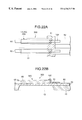
- FIG. 1 is an exploded perspective view of an ink jet recording head according to a first embodiment of the present invention
- FIGS. 2A and 2B are a plan view and a sectional view of the ink jet recording head according to the first embodiment of the present invention shown in FIG. 1;
- FIGS. 3A and 3B are drawings to show modified examples of a seal plate in FIG. 1;
- FIGS. 4A to 4 E are drawings to show a thin film manufacturing process in the first embodiment of the present invention.
- FIG. 5 is a drawing to show the thin film manufacturing process in the first embodiment of the present invention.
- FIGS. 6A and 6B are a plan view and a sectional view of the main part of the ink jet recording head according to the first embodiment of the present invention.
- FIG. 7 is a plan view to show a modified example of the ink jet recording head according to the first embodiment of the present invention.
- FIGS. 8A to 8 C are plan views to show modified examples of the ink jet recording head according to the first embodiment of the present invention.
- FIGS. 9A and 9B are a plan view and a sectional view to show a modified example of the ink jet recording head according to the first embodiment of the present invention.
- FIG. 10 is a sectional view of the main part of an ink, jet recording head according to a second embodiment of the present invention.
- FIGS. 11A to 11 D are drawings to show a thin film manufacturing process in the second embodiment of the present invention.
- FIG. 12 is a sectional view of the main part of an ink jet recording head according to a third embodiment of the present invention.
- FIGS. 13A and 13B are a plan view and a sectional view of the main part of an ink jet recording head according to a fourth embodiment of the present invention.
- FIGS. 14A to 14 C are drawings to show a thin film manufacturing process in the fourth embodiment of the present invention.
- FIGS. 15A and 15B are a plan view and a sectional view of the main part of an ink jet recording head according to a fifth embodiment of the present invention.
- FIG. 16 is a plan view of the main part to show a modified example of the ink jet recording head according to the fifth embodiment of the present invention.
- FIGS. 17A to 17 C are a plan view and sectional views of the main part of an ink jet recording head according to a sixth embodiment of the present invention.
- FIG. 18 is a plan view of the main part of an ink jet recording head according to a seventh embodiment of the present invention.
- FIGS. 19A and 19B are a plan view and a sectional view of the main part of an ink jet recording head according to an eighth embodiment of the present invention.
- FIGS. 20A and 20B are sectional views of the main parts to show modified examples of the ink jet recording head according to the eighth embodiment of the present invention.
- FIGS. 21A and 21B are a plan view and a sectional view of the main part of an ink jet recording head according to a ninth embodiment of the present invention.
- FIGS. 22A and 22B are a plan view and a sectional view of the main part of an ink jet recording head according to a tenth embodiment of the present invention.
- FIGS. 23A and 23B are a plan view and a sectional view of the main part of an ink jet recording head according to an eleventh embodiment of the present invention.
- FIG. 24 is an exploded perspective view to show an ink jet recording head according to another embodiment of the present invention.
- FIG. 25 is a sectional view to show the ink jet recording head shown in FIG. 24.
- FIG. 26 is a schematic diagram to show an ink jet recording apparatus according to one embodiment of the present invention.
- FIG. 1 is an exploded perspective view to show an ink jet recording head according to a first embodiment of the present invention.
- FIG. 2A is a plan view of the ink jet recording head shown in FIG. 1 and
- FIG. 2B is a sectional view to show the sectional structure in a longitudinal direction of one pressure generating chamber.
- a flow passage formation substrate 10 is made of a silicon monocrystalline substrate having ⁇ 110> direction of the crystal surface orientation in the embodiment. Normally, a substrate about 150-300 ⁇ m thick is used as the flow passage formation substrate 10 ; preferably a substrate about 180-280 ⁇ m thick, more preferably a substrate about 220 ⁇ m thick is used because the arrangement density can be made high while the rigidity of a partition between contiguous pressure generating chambers is maintained.
- the flow passage formation substrate 10 is formed on one face with an opening face and on an opposite face with an elastic film 50 of 0.1-2 ⁇ m thick made of silicon dioxide previously formed by thermal oxidation.
- the flow passage formation substrate 10 is formed on the opening face with nozzle openings 11 and pressure generating chambers 12 by anisotropically etching the silicon monocrystalline substrate.
- the anisotropic etching is executed by using the nature that if the silicon monocrystalline substrate is immersed in an alkaline solution such as KOH, it gradually erodes, a first ⁇ 111> plane perpendicular to a ⁇ 110> plane and a second ⁇ 111> plane forming about 70 degrees with the first ⁇ 111> plane and forming about 35 degrees with the ⁇ 110> plane appear, and the etching rate of the ⁇ 111> plane is about ⁇ fraction (1/180) ⁇ that of the ⁇ 110> plane.
- each pressure generating chamber 12 are formed by the first ⁇ 111> planes and the short sides are formed by the second ⁇ 111> planes.
- the pressure generating chambers 12 are formed by etching the silicon monocrystalline substrate to the elastic film 50 .
- the amount of immersing the elastic film 50 in the alkaline solution for etching the silicon monocrystalline substrate is extremely small.
- each nozzle opening 11 communicating with one end of each pressure generating chambers 12 is formed narrower and shallower than the pressure generating chamber 12 . That is, the nozzle openings 11 are made by etching the silicon monocrystalline substrate to an intermediate point in the thickness direction (half etching). The half etching is executed by adjusting the etching time.
- each pressure generating chamber 12 for giving ink drop jet pressure to ink and the size of each nozzle opening 11 for jetting ink drops are optimized in response to the jetted ink drop amount, jet speed, and jet frequency. For example, to record 360 ink drops per inch, the nozzle opening 11 needs to be made with accuracy with a groove width of several ten ⁇ m.
- the pressure generating chambers 12 and a common ink chamber 31 are made to communicate with each other via ink supply communication ports 21 formed at positions of a seal plate 20 (described later) corresponding to one end of the each pressure generating chamber 12 .
- Ink is supplied from the common ink chamber 31 through the ink supply communication ports 21 to the pressure generating chambers 12 .
- the seal plate 20 is made of glass ceramic having a thickness of 0.1-1 mm and a linear expansion coefficient of 2.5-4.5 ⁇ 10 ⁇ 6 [/° C.] at 300° C. or less, for example, formed with the ink supply communication ports 21 corresponding to the pressure generating chambers 12 .
- the ink supply communication ports 21 may be one slit hole 21 A or a plurality of slit holes 21 B crossing the neighborhood of the ink supply side ends of the pressure generating chambers 12 as shown in FIG. 3A or 3 B.
- One face of the seal plate 20 fully covers one face of the flow passage formation substrate 10 , namely, the seal plate 20 also serves as a reinforcing plate for protecting the silicon monocrystalline substrate from shock and external force.
- An opposite face of the seal plate 20 forms one wall face of the common ink chamber 31 .
- a common ink chamber formation substrate 30 forms a peripheral wall of the common ink chamber 31 ; it is made by stamping a stainless steel having a proper thickness responsive to the number of nozzle openings and the ink drop jet frequency.
- the common ink chamber formation substrate 30 is 0.2 mm thick.
- An ink chamber side plate 40 is made of a stainless substrate and one face thereof forms one wall face of the common ink chamber 31 .
- the ink chamber side plate 40 is formed with a thin wall 41 by forming a recess 40 a by half etching a part of an opposite face, and is punched to make an ink introduction port 42 for receiving ink supply from the outside.
- the thin wall 41 is adapted to absorb pressure toward the opposite side to the nozzle openings 11 occurring when ink drops are jetted; it prevents unnecessary positive or negative pressure from being applied to another pressure generating chamber 12 via the common ink chamber 31 .
- the ink chamber side plate 40 is 0.2 mm thick and a part thereof is made the thin wall 41 of 0.02 mm thick.
- the ink chamber side plate 40 may be made 0.02 mm thick from the beginning.
- an insulation film 55 for example, 0.1-2 ⁇ m thick is formed on the elastic film 50 on the opposite side to the opening face of the flow passage formation substrate 10 , and further a lower electrode film 60 , for example, about 0.2-0.5 ⁇ m thick, a piezoelectric film 70 , for example, about 1 ⁇ m thick, and an upper electrode film 80 , for example, about 0.1 ⁇ m thick are deposited on the insulation film 55 by a process described later, making up a piezoelectric element 300 .
- This piezoelectric element 300 refers to the portion containing the lower electrode film 60 , the piezoelectric film 70 , and the upper electrode film 80 .
- one electrode of the piezoelectric element 300 is used as a common electrode and the other electrode and the piezoelectric film 70 are patterned so as to correspond to each pressure generating chamber 12 .
- a portion made up of the patterned electrode and the piezoelectric film 70 where piezoelectric distortion occurs as voltage is applied to both electrodes is referred to as an active part 320 of the piezoelectric element 300 .
- the lower electrode film 60 is used as the common electrode of the piezoelectric element 300 and the upper electrode film 80 is used as a discrete electrode of the piezoelectric element 300 , but the lower electrode film 60 may be used as a discrete electrode and the upper electrode film 80 may be used as the common electrode for convenience of a drive circuit and wiring.
- the piezoelectric active part is formed for each pressure generating chamber 12 .
- the piezoelectric element 300 and the elastic film displaced by drive of the piezoelectric element 300 are collectively called a piezoelectric actuator.
- the lower electrode film 60 is patterned, thus the elastic film 50 and the insulation film 55 act as a diaphragm.
- a process of forming the piezoelectric films 70 , etc., on the flow passage formation substrate 10 made of a silicon monocrystalline substrate will be discussed with reference to FIG. 4 .
- a wafer of a silicon monocrystalline substrate of which the flow passage formation substrate 10 will be made is thermally oxidized in a diffusion furnace at about 1100° C. to form the elastic film 50 made of silicon dioxide.
- the insulation film 55 is formed on the elastic film 50 .
- the insulation film 55 is an intimate-contact insulation film made of a material having a good adhesion with the piezoelectric film 70 ; for example, it is formed of oxide or nitride of at least one element selected from among the elements of the piezoelectric film 70 .
- a zirconium layer is formed on the elastic film 50 , then thermal oxidation is executed in a diffusion furnace at about 500° C.-1200° C., for example, to form the insulation film 55 made of zirconium oxide.
- the lower electrode film 60 is formed by sputtering and is patterned in the areas corresponding to the pressure generating chambers 12 so that at least ends on both sides of each lower electrode film in the width direction thereof are positioned in the area facing the corresponding pressure generating chamber 12 .
- Pt, etc. is preferred as a material of the lower electrode film 60 , because the piezoelectric film 70 (described later) formed by a sputtering method or a sol-gel method needs to be baked and crystallized at a temperature of about 600° C.-1000° C. in air or an oxygen atmosphere after film formation. That is, the material of the lower electrode film 60 must be able to hold electrical conductivity in such a high-temperature, oxygen atmosphere. Particularly if PZT is used as the piezoelectric film 70 , it is desired that change in electrical conductivity caused by diffusion of PbO is less; Pt is preferred for the reasons.
- the piezoelectric film 70 is formed.
- a so-called sol-gel method is used wherein so-called sol including metal organic substance dissolved and dispersed in a solvent is applied and dried to gel and further the gel is baked at a high temperature, thereby providing the piezoelectric film 70 made of metal oxide.
- a lead zirconate titanate (PZT) family material is preferred as a material of the piezoelectric film 70 for use with an ink jet recording head.
- the formation method of the piezoelectric film 70 is not limited; for example, the piezoelectric film 70 may be formed by the sputtering method. In any way, the piezoelectric film 70 thus formed has crystal oriented unlike bulk piezoelectric substance.
- a precursor film of PZT is formed by the sol-gel method, the sputtering method, or the like, it may be crystal-grown at a low temperature by a high-pressure processing method in an alkaline solution.
- crystal direction thereof is preferentially oriented differently from piezoelectric bulk, and the crystal has a columnar structure.
- preferential orientation means a state wherein oriented direction of the crystal is not in disorder but specific crystal faces are almost oriented in a definite direction.
- columnar crystal structure means a state wherein cylindrical crystals are gathering in a surface direction thereof to form a thin film while central axes thereof are substantially coincident with each other in a thickness direction thereof.
- the thin film may be composed with preferentially oriented granular crystals.
- the thickness of the piezoelectric film manufactured by such thin film technique is 0.5-5 ⁇ m in general.
- the upper electrode film 80 is formed.
- the upper electrode film 80 may be made of any material if it has high electrical conductivity; for example, metal of Al, Au, Ni, Pt, etc., conductive oxide, etc., can be used.
- the upper electrode film 80 is formed of Pt by the sputtering method.
- the piezoelectric film 70 and the upper electrode film 80 are etched in batch for patterning the whole and the piezoelectric active parts 320 .
- patterning is executed so that the each piezoelectric film 70 covers at least side faces at both ends of the associated lower electrode film 60 in the width direction thereof and that both ends of the piezoelectric film 70 in the width direction thereof are positioned within an area facing the associated pressure generating chamber 12 .
- FIGS. 6A and 6B are a plan view and a sectional view to show the main part of the ink jet recording head of the embodiment thus formed.
- each of the piezoelectric element 300 consisting of the lower electrode film 60 , the piezoelectric film 70 , and the upper electrode film 80 is placed in an area corresponding to the associated pressure generating chamber 12 and each of the active part 320 of the piezoelectric element 300 consisting of the lower electrode film 60 the piezoelectric film 70 and the upper electrode film 80 is formed in an area facing the associated pressure generating chamber 12 and being out of contact with the peripheral wall.
- the lower electrode film 60 is patterned, thus the stress relaxation amount of the lower electrode film after the pressure generating chamber is formed is lessened and the initial deflection amount can be decreased as compared with the conventional structure wherein the lower electrode film is not patterned at the piezoelectric film formation time.
- Each of the lower electrode film 60 used as one electrode of the piezoelectric element 300 is extended from one end in the longitudinal direction of the associated pressure generating chamber 12 to the top of the peripheral wall thereof and the lower electrode films 60 extended from the respective piezoelectric elements 300 are joined on the top of the peripheral wall as common electrode to the piezoelectric elements 300 , and connected to external wiring in the proximity of the end (not shown).
- Each of the upper electrode film 80 used as the other electrode of the piezoelectric element 300 is extended together with the associated piezoelectric film 70 from one end in the longitudinal direction of the associated pressure generating chamber 12 (in the embodiment, from the end on the opposite side to the extending direction of the lower electrode film 60 ) to the top of the peripheral wall, and external wiring (not shown) is connected in the proximity of the end of the upper electrode film 80 so that voltage can be applied for each active part 320 of the piezoelectric element 300 .
- the lower electrode film 60 and the upper electrode film 80 are extended to the top of the peripheral wall in the opposite directions from the end in the longitudinal direction of the pressure generating chamber 12 , so that wiring can be drawn without using an inter-layer insulating film or a contact hole, and displacement efficiency and durability can be improved.
- the each lower electrode film 60 is formed so that both ends in the width direction are positioned within the area facing the associated pressure generating chamber 12 , and both ends of the lower electrode film 60 in the width direction thereof are covered with the associated piezoelectric film 70 .
- the piezoelectric film 70 covering both ends of the lower electrode film 60 in the width direction thereof and the insulation film 55 are formed so that they are adhered with each other.
- both sides of the lower electrode film 60 vibrated during driving are completely covered with the corresponding piezoelectric film 70 , so that the strength of the dielectric breakdown thereon is improved and thereby the dielectric breakdown of the piezoelectric film 70 can be prevented.
- the strength of the dielectric breakdown is low because the piezoelectric film 70 is manufactured by the thin-film technique so the thickness thereof as to be thin, the strength of the dielectric breakdown of the piezoelectric film 70 can remarkably improved to surely prevent the electric breakdown thereof by adopting such configuration. Further, since the piezoelectric film 70 and the insulation film 55 are brought completely into intimate contact with each other, the initial deflection amount of the diaphragm is decreased.
- the upper electrode film 80 is formed on the piezoelectric film 70 so that the relationship among width W TE of the upper electrode film 80 , width W BE of the lower electrode film 60 , and thickness T of the piezoelectric film 70 becomes
- an electric field produced when a voltage is applied to the part between the upper electrode film 80 and the lower electrode film 60 acts effectively on the piezoelectric film 70 and the active part 320 of the piezoelectric element 300 can be driven effectively.
- both ends of the piezoelectric film 70 in the width direction thereof are positioned in the area facing the pressure generating chamber 12 , but the present invention is not limited to this configuration.
- they may be positioned on the tops of the partitions on both sides in the width direction of the pressure generating chamber 12 .
- the insulation film 55 is formed of one layer of only the intimate-contact insulation film, but the present invention is not limited to this configuration.
- the insulation film 55 may be formed of two or more layers, in which case preferably, the top layer is an intimate-contact insulation film.
- the intimate-contact insulation film may be formed of multiple layers, needless to say.
- each flow passage formation substrate 10 is bonded to the seal plate 20 , the common ink chamber formation substrate 30 , and the ink chamber side plate 40 in order in one piece to form an ink jet recording head.
- ink is taken in through the ink introduction port 42 connected to external ink supplier (not shown) and the inside of the recording head from the common ink chamber 31 to the nozzle openings 11 is filled with ink, then a voltage is applied to the part between the lower electrode film 60 and the upper electrode film 80 according to a record signal from an external drive circuit (not shown) for deflection-deforming the elastic film 50 , the insulation film 55 , the lower electrode film 60 , and the piezoelectric film 70 , thereby raising pressure in the pressure generating chamber 12 and jetting an ink drop through the nozzle opening 11 .
- the lower electrode film 60 is extended from the end in the longitudinal direction of the pressure generating chamber 12 to the top of the peripheral wall, but the present invention is not limited to this configuration.
- a wider portion 60 a wider than the pressure generating chamber 12 may be provided in that area of the each lower electrode film 60 corresponding to the boundary between the pressure generating chamber 12 and the peripheral wall, and the area may be covered therewith.
- the lower electrode films of the adjacent piezoelectric elements are joined by the wider portions 60 a.
- the lower electrode film 60 is used as the common electrode and the upper electrode film 80 and the lower electrode film 60 are extended from the opposite ends in the longitudinal direction, but the present invention is not limited to this configuration.
- the upper electrode film 80 may be used as the common electrode and the upper electrode film 80 and the lower electrode film 60 may be extended from the opposite ends in the longitudinal direction to the top of the peripheral wall as in the embodiment.
- the lower electrode film 60 for example, as the common electrode may be extended from the end in the longitudinal direction of the pressure generating chamber 12 to the top of the outer peripheral wall in the width direction.
- the position at which the lower electrode film 60 crosses the end of the pressure generating chamber 12 is within the dimension of the width thereof from the end in the longitudinal direction of the pressure generating chamber 12 so as not to interface with displacement caused by drive of the active part 320 of the piezoelectric element 300 .
- a voltage is applied to the part between the upper electrode film 80 and the lower electrode film 60 , thereby driving the piezoelectric film 70 in the area sandwiched between the upper electrode film 80 and the lower electrode film 60 in the area facing the pressure generating chamber 12 .
- similar advantages to those described above can also be provided. In fact, only the active part 320 of the piezoelectric element 300 in the area facing the pressure generating chamber 12 is driven, so that the displacement efficiency can be improved.
- the upper electrode film 80 and the lower electrode film 60 may be extended from the same end in the longitudinal direction of the pressure generating chamber 12 to the top of the peripheral wall.
- the lower electrode film 60 , the upper electrode film 80 , and the piezoelectric film 70 making up the active part 320 of the piezoelectric element 300 in the area facing the pressure generating chamber 12 are extended continuously to the area facing the peripheral wall; except this point, however, similar advantages to those described above can be provided.
- the lower electrode film 60 may be used as a discrete electrode and be extended from one end in the longitudinal direction to the top of the peripheral wall of the pressure generating chamber 12 for each active part 320 of the piezoelectric element 300 and the upper electrode film 80 may be formed continuously on the piezoelectric active parts 320 placed side by side in the width direction as the common electrode to the piezoelectric active parts 320 .
- This configuration can be provided by forming the upper electrode film 80 after patterning the piezoelectric film 70 , then patterning only the upper electrode film 80 . According to the configuration, similar advantages to those described above can also be provided.
- the upper electrode film 80 is formed continuously on the piezoelectric active parts 320 placed side by side in the width direction, whereby it is also formed in the area facing so-called diaphragm arm parts on both sides in the width direction of the active part 320 of the piezoelectric element 300 ; the strength of the arm parts is enhanced.
- FIG. 10 is a sectional view of the main part of an ink jet recording head according to a second embodiment of the present invention.
- the second embodiment is the same as the first embodiment except that an insulation thick film portion 55 a thicker than any other area is formed under the formation area of a lower electrode film 60 .
- similar advantages to those of the first embodiment can also be provided. Since a piezoelectric film 70 is positioned apart from the neutral axis of displacement caused by drive of a piezoelectric element 300 , the displacement efficiency is improved and the exclusion volume can be improved.
- a film formation process of the second embodiment will be discussed with reference to FIG. 11 .
- the process of forming an elastic film 50 , an insulation film 55 , and a lower electrode film 60 on a flow passage formation substrate 10 is similar to that of the first embodiment.
- the lower electrode film 60 and the insulation film 55 are etched for patterning.
- the insulation film 55 is etched to an intermediate point in the thickness direction (half etched). That is, the area where the lower electrode film 60 does not exist is made thin to form an insulation thin film portion 55 b , whereby an insulation thick film portion 55 a thicker than any other portion can be formed under the area where the lower electrode film 60 exits.
- a piezoelectric film 70 and an upper electrode film 80 are formed.
- the piezoelectric film 70 and the upper electrode film 80 are etched for patterning the whole and piezoelectric active parts 320 .
- the later steps of the process are similar to those of the first embodiment.
- FIG. 12 is a sectional view to show the main part of an ink jet recording head according to a third embodiment of the present invention.
- the third embodiment is the same as the first embodiment except that an elastic film removal part 350 where an elastic film 50 is removed is provided in the area corresponding to a pressure generating chamber 12 and except that an insulation film 55 and a lower electrode film 60 constitute a diaphragm.
- the formation method of the elastic film removal parts 350 are not limited to a specific process; for example, the elastic film removal parts 350 may be formed by etching, etc., after the pressure generating chambers 12 are formed.
- the elastic film removal parts 350 are provided, the arm parts of the diaphragm are formed only of the insulation film 55 , so that the diaphragm displacement efficiency caused by drive of an active part 320 of the piezoelectric element 300 is improved and the exclusion volume can be improved.
- the elastic film removal parts 350 are made in the elastic film 50 after the pressure generating chambers 12 are formed.
- the present invention is not limited to this configuration; for example, without providing the elastic film 50 from the beginning, the insulation film 55 may be formed directly on a flow passage formation substrate 10 and the diaphragm may be formed only of the insulation film 55 .
- the area of the insulation film 55 facing the lower electrode film may be made thicker than any other portion as in the second embodiment, needless to say.
- FIGS. 13A and 13B are a plan view and a sectional view to show the main part of an ink jet recording head according to a fourth embodiment of the present invention.
- the fourth embodiment is the same as the first embodiment except that a piezoelectric film 70 is provided continuously from the area facing a pressure generating chamber 12 to partitions on both sides in the width direction.
- an active part 320 of the piezoelectric element 300 consisting of a lower electrode film 60 , a piezoelectric thick film part 70 a and an upper electrode film 80 are provided in the area facing each pressure generating chamber 12 and on both sides in the width direction of the active part 320 of the piezoelectric element 300 , a piezoelectric thin film part 70 b thinner than the piezoelectric thick film part 70 a is extended continuously to the outside of the area facing the pressure generating chamber 12 .
- both sides of the lower electrode film 60 vibrated during driving are completely covered with the piezoelectric film 70 , so that strength of the dielectric breakdown is improved remarkably. Since the piezoelectric film 70 b and the insulation film 55 are brought completely into intimate contact with each other, the initial deflection amount of the diaphragm is decreased.
- the piezoelectric film 70 continuously from the pressure generating chamber 12 to the top of a peripheral wall as in the fourth embodiment preferably the crystalline structure of the piezoelectric film 70 on the lower electrode film 60 is the same as that on the insulation film 55 .
- the piezoelectric film 70 is formed as follows:
- crystal seed 75 made of titanium or titanium oxide is formed like islands on the lower electrode film 60 and the insulation film 55 by the sputtering method, then uncrystallized piezoelectric precursor layer 71 is formed as shown in FIG. 14B, then baked for crystallization to form the piezoelectric film 70 as shown in FIG. 14 C.
- the crystal seed on the insulation film 55 may be formed at the same time after the lower electrode film 60 is patterned. Alternatively, after crystal seed on the lower electrode film 60 is formed and patterning is executed, crystal seed may be formed separately on the insulation film 55 only. In the embodiment, the crystal seed is formed like islands, but the present invention is not limited to this configuration; for example, the crystal seed may be formed like a film.
- the lower electrode film 60 used as one electrode of the active part 320 of the piezoelectric element 300 is extended from one end in the longitudinal direction to the top of the peripheral wall of the pressure generating chamber 12 and the lower electrode film 60 extended from each active part 320 of the piezoelectric element 300 is joined on the top of the peripheral wall to form a common electrode to the respective piezoelectric active parts 320 , which is connected to external wiring (not shown) in an installation part 60 c in the proximity of the end of a common part 60 b.
- the piezoelectric film is formed using the sol-gel method in the embodiment, the difference in level on the surface of the piezoelectric film 70 before etching is formed small and the piezoelectric film 70 in the area which becomes the piezoelectric thin film part 70 b after etching becomes comparatively thick. Therefore, if an attempt is made to pattern the piezoelectric film 70 in the area facing the pressure generating chamber 12 , the common portion must be exposed in a separate step; however, the piezoelectric thin film part 70 b is formed, whereby the installation part 60 c in the common portion can also be exposed at the same time.
- FIGS. 15A and 15B are a plan view and a sectional view of the main part of an ink jet recording head according to a fifth embodiment of the present invention.
- the fifth embodiment is an example wherein a discontinuous lower electrode film 61 discontinuous with a lower electrode film 60 is formed below a piezoelectric film 70 in the area facing the boundary between one end and the peripheral wall of a pressure generating chamber 12 . That is, in the embodiment, in the proximity of the end of the side of the pressure generating chamber 12 where the piezoelectric film 70 and an upper electrode film 80 are extended, a lower electrode film removal part 330 where the lower electrode film 60 is removed is provided, for example, like a narrow groove in the direction in which the pressure generating chambers 12 are placed side by side along the form thereof. The lower electrode film in the boundary between the end and the peripheral wall of each pressure generating chamber 12 becomes the discontinuous lower electrode film 61 discontinuous with the lower electrode film 60 of an active part 320 of the piezoelectric element 300 .
- each wiring lower electrode film 62 used as wiring of each active part 320 of the piezoelectric element 300 is provided by patterning the lower electrode film 60 separately for each active part 320 of the piezoelectric element 300 .
- the piezoelectric film 70 and the upper electrode film 80 are extended onto the wiring lower electrode film 62 via the top of the discontinuous lower electrode film 61 , and they are connected by a lead electrode 100 .
- the lower electrode film 60 is formed directly on an elastic film 50 without providing an insulation film 55 on the elastic film 50 .
- the width of the lower electrode film removal part 330 separating the lower electrode film 60 and the discontinuous lower electrode film 61 needs to be a width at least capable of holding the insulating strength between the lower electrode film 60 and the discontinuous lower electrode film 61 ; however, preferably the lower electrode film removal part 330 is made narrow as much as possible for holding the rigidity of a diaphragm.
- the discontinuous lower electrode film 61 becomes a floating electrode not electrically connected to any other parts
- the piezoelectric film 70 and the upper electrode film 80 disposed on the lower electrode film 60 constitute the active part 320 of the piezoelectric element 300 which becomes a substantial drive part
- the piezoelectric film 70 and the upper electrode film 80 on the discontinuous lower electrode film 61 are not strongly driven.
- the boundary between the pressure generating chamber 12 and the peripheral wall is not strongly driven if a voltage is applied to the active part 320 of the piezoelectric element 300 , thus the rigidity of the diaphragm at the end of the longitudinal direction of the pressure generating chamber 12 is high and destruction of the diaphragm or the piezoelectric film 70 or the like in the portion can be prevented.
- the discontinuous lower electrode film 61 is formed over the area in the direction in which the pressure generating chambers 12 are placed side by side, but the present invention is not limited to this configuration.
- separate discontinuous lower electrode films 61 may be provided in a one-to-one correspondence with the piezoelectric active parts 320 , whereby the piezoelectric film 70 and the upper electrode film 80 on the discontinuous lower electrode film 61 are not driven at all and destruction of the diaphragm or the piezoelectric film 70 or the like can be prevented more reliably.
- the discontinuous lower electrode film 61 is a floating electrode not electrically connected to any other parts, but the present invention is not limited to this configuration.
- the discontinuous lower electrode film 61 may be connected to an electrode layer via a resistor having a predetermined resistance value so that time constant for charging becomes larger than the drive pulse of the active part 320 of the piezoelectric element 300 .
- FIGS. 17A to 17 C are a plan view and sectional views of the main part of an ink jet recording head according to a sixth embodiment of the present invention.
- the sixth embodiment is an example wherein a remaining part 63 made of the same layer as a lower electrode film 60 is provided on the top of a partition in the width direction of a pressure generating chamber 12 .
- the remaining part 63 is provided in the longitudinal direction of the pressure generating chamber 12 continuously with the lower electrode film 60 of an active part 320 of the piezoelectric element 300 . That is, lower electrode film removal parts 330 with the lower electrode film 60 removed are provided in the areas facing the boundaries with the partitions on both sides in the width direction of the pressure generating chamber 12 , whereby the remaining part 63 is formed in the area facing the partition.
- spacing h 1 between the side at the end in the width direction of the lower electrode film 60 and the side at the end in the width direction of the remaining part 63 and spacing h 2 between the side at the end in the longitudinal direction of the piezoelectric film 70 and the part where the lower electrode film 60 extended to the top of the peripheral wall becomes wide are wider than the film thickness of the piezoelectric film 70 and narrower than the width of the lower electrode film 60 .
- the width of the remaining part 63 is 50% or more of the width of the partition; more preferably 80% or more. Further, preferably the lower electrode film 60 or the remaining part 63 is formed in the area of at least 50% or more of the area facing the pressure generating chambers 12 placed side by side and the partitions on both sides in the width direction of the pressure generating chambers 12 .
- the lower electrode film 60 is separated by the lower electrode film removal part 330 where the lower electrode film 60 is removed like a narrow groove in the direction in which the pressure generating chambers 12 are placed side by side, and the lower electrode film in the area facing the peripheral wall of each pressure generating chamber 12 becomes a discontinuous lower electrode film 61 discontinuous with the lower electrode film 60 forming a part of the active part 320 of the piezoelectric element 300 .
- the piezoelectric film 70 and the upper electrode film 80 are extended onto the discontinuous lower electrode film 61 and the upper electrode film 80 and external wiring are connected in the proximity of the end (not shown).
- the remaining part 63 is provided in the area facing the partitions on both sides in the width direction of the pressure generating chamber 12 preferably under the above-described condition, so that the lower electrode film 60 removal area very lessens and if the piezoelectric film 70 is formed on the patterned lower electrode film 60 , the film thickness of the piezoelectric film 70 becomes substantially uniform on the whole and the piezoelectric film 70 does not become locally thin.
- the film thickness of the piezoelectric film 70 becomes uniform even in the proximity of the end in the longitudinal direction of the pressure generating chamber 12 .
- a nonselective etching method such as ion milling to etch the piezoelectric film 70 in the proximity of the end of the side of the pressure generating chamber 12 where the lower electrode film 60 is drawn, the lower electrode film 60 below the piezoelectric film 70 is not removed together and does not become thin.
- the rigidity of the lower electrode film 60 in the proximity of the end of the side of the pressure generating chamber 12 is not degraded and the durability is enhanced.
- FIG. 18 is a plan view of the main part of an ink jet recording head according to a seventh embodiment of the present invention.
- the seventh embodiment is the same as the sixth embodiment except that a remaining part 63 provided on the top of a peripheral wall in the width direction of a pressure generating chamber 12 is provided continuously with a discontinuous lower electrode film 61 rather than a lower electrode film 60 forming a part of an active part 320 of the piezoelectric element 300 .
- a piezoelectric film 70 does not become thin and similar advantages to those of the sixth embodiment can be provided.
- the remaining part 63 is provided continuously with the lower electrode film 60 forming a part of a piezoelectric element 300 or the discontinuous lower electrode film 61 , but the present invention is not limited to this configuration.
- the remaining part 63 may be provided independently.
- the remaining part 63 is always left, but the present invention is not limited to this configuration. After the piezoelectric element 300 is formed, the remaining part 63 may be removed. Even in such a configuration, the film thickness of the piezoelectric film 70 is formed substantially uniform, thus similar advantages to those of the above-described embodiment can be provided, of course.
- FIGS. 19A and 19B are a plan view and a sectional view of the main part of an ink jet recording head according to an eighth embodiment of the present invention.
- the eighth embodiment is an example wherein a film tapering part 64 where the film thickness of a lower electrode film 60 is gradually decreased toward the outside of an active part 320 of the piezoelectric element 300 is provided at the end of the lower electrode film 60 forming a part of an active part 320 of the piezoelectric element 300 .
- the form of the film tapering part 64 is not limited to a specific shape; for example, in the embodiment, the film tapering part 64 forms a slope where the film thickness of the lower electrode film 60 is gradually decreased continuously.
- a wiring lower electrode film 62 used as wiring of each active part 320 of the piezoelectric element 300 is provided by patterning the lower electrode film 60 separately for each active part 320 of the piezoelectric element 300 .
- a piezoelectric film 70 and an upper electrode film 80 are patterned in the area facing a pressure generating chamber 12 and the upper electrode film 80 and the wiring lower electrode film 62 are connected by a lead electrode 100 .
- the film tapering part 64 where the film thickness is gradually decreased toward the outside of the active part 320 of the piezoelectric element 300 is provided at the end of the lower electrode film 60 as the end of the active part 320 of the piezoelectric element 300 , thus if the piezoelectric film 70 is formed on the lower electrode film 60 containing the film tapering part 64 , it is formed along the form of the lower electrode film 60 and the whole film thickness becomes substantially uniform. That is, the piezoelectric film 70 at the end of the lower electrode film 60 does not become thin and dielectric breakdown of the piezoelectric film 70 caused by concentration of electric field, etc., in the proximity of the end of the active part 320 of the piezoelectric element 300 can be prevented.
- the film tapering part 64 is made a slope where the film thickness is gradually decreased continuously, but the present invention is not limited to this configuration.
- a film tapering part 64 A may be provided with the film thickness decreased stepwise in cross section.
- the formation method of the film tapering part 64 A is not limited either; for example, a resist is applied more than once and a resist film shaped stepwise substantially the same form as the film tapering part 64 A is formed in the area of the lower electrode film 60 where the film tapering part 64 A is to be formed, then the lower electrode film 60 is patterned, whereby the film tapering part 64 A can be formed.
- a film tapering part 64 B may be provided as a slanting curved surface in cross section.
- the formation method of the film tapering part 64 B is not limited either; for example, the area on the elastic film 50 where the lower electrode film 60 is not formed and the area where the film tapering part 64 B is to be formed are masked and the lower electrode film 60 is formed by so-called mask evaporation, whereby the film tapering part 64 B is formed. That is, the lower electrode film 60 is also formed in a part of the mask area from a mask gap, providing the film tapering part 64 B which is a slanting curved surface in cross section.
- a resist film of substantially the same form as the film tapering part 64 B is formed on the lower electrode film 60 , then the lower electrode film 60 is patterned, whereby the film tapering part 64 B can be formed.
- the piezoelectric film 70 and the upper electrode film 80 are patterned in the area facing the pressure generating chamber 12 , but they may be extended onto the wiring lower electrode film 62 , of course.
- the upper electrode film 80 and the wiring lower electrode film 62 are connected by the lead electrode 100 , but the present invention is not limited to this configuration.
- the piezoelectric film 70 and the upper electrode film 80 may be extended onto the wiring lower electrode film 62 for connecting the upper electrode film 80 and the wiring lower electrode film 62 directly.
- FIGS. 21A and 21B are a plan view and a sectional view of the main part of an ink jet recording head according to a ninth embodiment of the present invention.
- the ninth embodiment is an example wherein an insulating film made of an insulating material is provided on the outside in the longitudinal direction of a lower electrode film 60 . That is, as shown in FIG. 21, the ninth embodiment is similar to the eighth embodiment except that an active part 320 of the piezoelectric element 300 consisting of a lower electrode film 60 , a piezoelectric film 70 and an upper electrode film 80 are formed on an elastic film 50 in the area facing each pressure generating chamber 12 and except that a second insulating film 65 having substantially the same film thickness as the lower electrode film 60 is formed, for example, on the outside of the end of the lower electrode film 60 , which is the end of the active part 320 of the piezoelectric element 300 .
- the material of the second insulating film 65 is not limited; for example, it may be an insulating material different from that of an insulating film 55 .
- the second insulating film 65 is formed on a lower electrode film removal part 330 provided on the outside in one end of the lower electrode film 60 in the longitudinal direction thereof, and the piezoelectric film 70 and the upper electrode film 80 are formed and patterned on the second insulating film 65 , forming the active part 320 of the piezoelectric element 300 , whereby the piezoelectric film 70 does not become thin at the end of the lower electrode film 60 , and dielectric breakdown of the piezoelectric film 70 caused by concentration of electric field, etc., in the portion can be prevented. Even in such a configuration, similar advantages to those of the above-described embodiment can be provided, of course.
- FIGS. 22A and 22B are a plan view and a sectional view of the main part of an ink jet recording head according to a tenth embodiment of the present invention.
- the tenth embodiment is similar to the ninth embodiment except that a thick film part 51 thicker than any other portion of an elastic film 50 (for example, in the embodiment, placed almost at the same height as a lower electrode film 60 ) is provided on the outside of an end of the lower electrode film 60 , which is an end of an active part 320 of the piezoelectric element 300 , in place of a second insulating film 65 .
- a piezoelectric film 70 and an upper electrode film 80 are formed and patterned, thereby forming the active part 320 of the piezoelectric element 300 , whereby the piezoelectric film 70 in the area corresponding to the end of the lower electrode film 60 does not become thinner than any other portion, and dielectric breakdown of the piezoelectric film 70 caused by concentration of electric field, etc., in the portion can be prevented. Even in such a configuration, similar advantages to those of the above-described embodiment can be provided, of course.
- FIGS. 23A and 23B are a plan view and a sectional view of the main part of an ink jet recording head according to an eleventh embodiment of the present invention.
- the eleventh embodiment is an example wherein an end of an upper electrode film 80 is formed inside from an end of a lower electrode film 60 and becomes an end of an active part 320 of the piezoelectric element 300 .
- the piezoelectric film 70 is also formed on the lower electrode film 60 projecting to the outside from the end of the upper electrode film 80 , but this portion constitutes a piezoelectric inactive part 340 not substantially driven.
- a wiring lower electrode film 62 is provided on the top of a peripheral wall of a pressure generating chamber 12 and is connected at one end to an external terminal (not shown) and is connected to the upper electrode film 80 of the active part 320 of the piezoelectric element 300 by a lead electrode 100 extended onto the piezoelectric inactive part 340 .
- the piezoelectric film 70 is not removed and remains and the lower electrode film 60 and the lead electrode 100 are insulated from each other.
- the piezoelectric inactive part 340 is provided continuously, for example, by removing the upper electrode film 80 , whereby the distance between the end of the upper electrode film 80 , which is the end of the active part 320 of the piezoelectric element 300 , and the end of the lower electrode film 60 can be made large.
- the electric field strength at the end of the active part 320 of the piezoelectric element 300 does not grow and dielectric breakdown of the piezoelectric film 70 , etc., can be prevented. Since the thickness of the piezoelectric film 70 of the active part 320 of the piezoelectric element 300 becomes uniform, the piezoelectric characteristic is improved. Even in such a configuration, similar advantages to those of the above-described embodiment can be provided.
- the end of the lower electrode film 60 is the end of the active part 320 of the piezoelectric element 300 and the piezoelectric film 70 and the upper electrode film 80 on the lower electrode film 60 are extended to the outside of the end for preventing destruction of the active part 320 of the piezoelectric element 300 ; at the opposite end, the lower electrode film 60 is drawn to the top of the peripheral wall and the piezoelectric film 70 and the upper electrode film 80 are patterned in the pressure generating chamber 12 , thereby forming the end of the active part 320 of the piezoelectric element 300 .
- peeling, etc., of the piezoelectric film 70 and the upper electrode film 80 may occur at the end.
- the end of the active part 320 of the piezoelectric element 300 may be fixed with an adhesive, etc., or be covered with a discontinuous piezoelectric film discontinuous with the piezoelectric film 70 of the piezoelectric element 300 or the like, whereby it is protected for enhancing durability.
- the structure of the side of one end of the active part 320 of the piezoelectric element 300 is described, but the present invention is not limited to this configuration.
- a similar structure may be adopted for the opposite end of the active part 320 of the piezoelectric element 300 .
- the common ink chamber formation plate 30 may be made of glass ceramic and further the thin wall 41 may be made of glass ceramic as a separate member; the material, structure, etc., can be changed as desired.
- the nozzle openings are made in the end face of the flow passage formation substrate 10 , but may be formed projecting in a direction perpendicular to the plane.
- FIG. 24 is an exploded perspective view of an embodiment of an ink jet recording head having such a configuration
- FIG. 25 is a sectional view to show a flow passage in the ink jet recording head.
- nozzle openings 11 are made in a nozzle substrate 120 opposed to piezoelectric vibrator and nozzle communication ports 22 for allowing the nozzle openings 11 and pressure generating chambers 12 to communicate with each other are placed so as to penetrate a seal plate 20 , a common ink chamber formation plate 30 , a thin plate 41 A, and an ink chamber side plate 40 A.
- the embodiment is basically similar to the above-described embodiments except that the thin plate 41 A and ink chamber side plate 40 A are separate members and except that an opening 40 b is made in the ink chamber side plate 40 A. Parts identical with those previously described with reference to the accompanying drawings are denoted by the same reference numerals in FIGS. 24 and 25 are will not be discussed again.
- the present invention can also be applied to ink jet recording heads of the type wherein a common ink chamber is formed in a flow passage formation substrate.
- Each of the ink jet recording heads of the embodiments forms a part of a recording head unit comprising an ink flow passage communicating with an ink cartridge, etc., and is installed in an ink jet recording apparatus.
- FIG. 26 is a schematic diagram to show an example of the ink jet recording apparatus.
- cartridges 2 A and 2 B forming a ink supply member are detachably placed in recording head units 1 A and 1 B each having an ink jet recording head, and a carriage 3 on which the recording head units 1 A and 1 B are mounted is placed so as to be axially movable on a carriage shaft 5 attached to a recorder main body 4 .
- the recording head units 1 A and 1 B jet a black ink composite and a color ink composite respectively, for example.
- the driving force of a drive motor 6 is transmitted to the carriage 3 via a plurality of gears and a timing belt (not shown), whereby the carriage 3 on which the recording head units 1 A and 1 B are mounted is moved along the carriage shaft 5 .
- the recorder main body 4 is provided with a platen 8 along the carriage shaft 5 and a recording sheet S of a recording medium such as paper fed by a paper feed roller, etc., (not shown) is wrapped around the platen 8 and is transported.
- the lower electrode film is patterned in the areas facing the pressure generating chambers and both ends in the width direction thereof are covered with the piezoelectric layer, so that the strength of the dielectric breakdown on a sidewall is improved.
- the piezoelectric film manufactured by the thin-film technique it is easily occurred the dielectric breakdown because such piezoelectric film has thin thickness.
- the electric breakdown of the piezoelectric film can be surely prevented.
- the initial deflection amount of the diaphragm at the time of forming the pressure generating chamber is decreased. Further, the width of the upper electrode film is formed within the predetermined range, thus lowering of the displacement efficiency of the piezoelectric active part by applying a voltage can be prevented. Therefore, the piezoelectric active part of each diaphragm can be driven efficiently.
- the piezoelectric film can be formed in a substantially uniform film thickness and degradation of the partial piezoelectric characteristic of the piezoelectric film can be suppressed. Further, since the film thickness of the piezoelectric film is substantially uniform, when the piezoelectric film is patterned at the end of the side of the pressure generating chamber where the lower electrode film is drawn, the lower electrode film does not become thin; destruction of the lower electrode film, etc., can be prevented and the durability is enhanced.
- the piezoelectric film in the proximity of the end of the lower electrode film does not become thinner than any other portion, and dielectric breakdown of the piezoelectric film caused by concentration of electric field, etc., can be prevented.
- wiring can be drawn easily without using an inter-layer insulating film or a contact hole, and the displacement efficiency and durability can be improved.
Abstract
An ink jet recording head comprises a pressure generating chamber communicating with a nozzle opening, and a piezoelectric element a lower electrode provided on an area facing the pressure generating chamber via an insulating layer, a piezoelectric layer provided on the lower electrode, and an upper electrode provided on the piezoelectric layer. At least both ends of the lower electrode in a width direction thereof are positioned within the area facing the pressure generating chamber, and the piezoelectric layer covers sides of both ends of the lower electrode in the width direction thereof.
Description
This invention relates to an ink jet recording head wherein a piezoelectric element is formed via a diaphragm in a part of each of pressure generating chambers communicating with nozzle openings for jetting ink drops and ink drops are jetted by displacement of the piezoelectric element, and an ink jet recording apparatus comprising the ink jet recording head.
The following two types of ink jet recording heads, each wherein a part of a pressure generating chamber communicating with a nozzle opening for jetting an ink drop is formed of a diaphragm and the diaphragm is deformed by a piezoelectric element for pressurizing ink in the pressure generating chamber for jetting an ink drop through the nozzle opening, are commercially practical: One uses a piezoelectric actuator in a vertical vibration mode in which the piezoelectric element is expanded and contracted axially and the other uses a piezoelectric actuator in a deflection vibration mode.
With the former, the volume of the pressure generating chamber can be changed by abutting an end face of the piezoelectric element against the diaphragm and a head appropriate for high-density printing can be manufactured, but a difficult step of dividing the piezoelectric element like comb teeth matching the arrangement pitch of the nozzle openings and work of positioning and fixing the piezoelectric element divisions in the pressure generating chambers are required and the manufacturing process is complicated.
In contrast, with the latter, the piezoelectric element can be created and attached to the diaphragm by executing a comparatively simple process of putting a green sheet of a piezoelectric material matching the form of the pressure generating chamber and baking it, but a reasonable area is required because deflection vibration is used; high-density arrangement is difficult to make.
On the other hand, to solve the problem of the latter recording head, Japanese Patent Publication No. 5-286131A proposes an art wherein an uniform piezoelectric material layer is formed over the entire surface of a diaphragm according to a film formation technique and is divided to a form corresponding to a pressure generating chamber according to a lithography technique for forming a piezoelectric element separately for each pressure generating chamber.
This eliminates the need for work of putting the piezoelectric element on the diaphragm and the piezoelectric element can be created by the lithography method, an accurate and simple technique. In addition, the piezoelectric element can be thinned and high-speed drive is enabled.
However, in the manufacturing method according to the thin-film technique and the lithography method described above, after thin film patterning, pressure generating chambers are formed. At the time, a diaphragm is deflected to the pressure generating chamber side by the effect of relaxation of the internal stresses in an upper electrode and piezoelectric layers and the deflection remains as the initial deformation of the diaphragm.
Further, in a piezoelectric vibrator manufactured by the thin-film technique and the lithography method, in which arm portions of a lower electrode are removed by the patterning, a piezoelectric layer becomes thinner. Thus, the strength of the dielectric breakdown on both sidewalls in width direction of the lower electrode becomes lower and thereby the dielectric breakdown occurs easily.
It is therefore an object of the present invention to provide an ink jet recording head, wherein the dielectric breakdown of the piezoelectric layer is prevented and wherein the initial deflection amount of a diaphragm is decreased, and an ink jet recording apparatus comprising the ink jet recording head.
In order to achieve the above object, according to a first aspect of the present invention, there is provided an ink jet recording head comprising: a pressure generating chamber communicating with a nozzle opening; and a piezoelectric element a lower electrode provided on an area facing the pressure generating chamber via an insulating layer, a piezoelectric layer provided on the lower electrode, and an upper electrode provided on the piezoelectric layer, wherein at least both ends of the lower electrode in a width direction thereof are positioned within the area facing the pressure generating chamber, and the piezoelectric layer covers sides of both ends of the lower electrode in the width direction thereof.
In the first aspect, the both side wall of the lower electrode in the width direction thereof patterned in the pressure generating chamber are covered with the piezoelectric layer, thus the strength of the dielectric breakdown thereon is improved and the insulating layer and the piezoelectric layer are brought into intimate contact with each other, whereby the initial deflection amount of a diaphragm is decreased.
According to a second aspect of the present invention, in the ink jet recording head of the first aspect, crystal direction of the piezoelectric layer is preferentially oriented.
In the second aspect, the piezoelectric layer is formed in a thin film process, so that crystal is preferentially oriented.
According to a third aspect of the present invention, in the ink jet recording head of the second aspect, the piezoelectric layer has a columnar crystal structure.
In the third aspect, the piezoelectric layer is formed in a thin film process, so that the piezoelectric layer has a columnar crystal structure.
According to a fourth aspect of the present invention, in the ink jet recording head of the first to third aspect, the insulating layer in the area under the area where the lower electrode is formed is thicker than any other area.
In the fourth aspect, the piezoelectric layer is at a position distant from the neutral axis of bend caused by drive of the piezoelectric element, so that displacement efficiency is improved.
According to a fifth aspect of the present invention, in the ink jet recording head of any of the first to fourth aspects, the top of the insulating layer in a thickness direction thereof is made of an adhesive insulating layer made of a material having a good adhesion with the piezoelectric layer. The adhesive insulating layer is adhered with the piezoelectric layer covering sides of both ends of the lower electrode in the width direction thereof.
In the fifth aspect, the lower electrode in the area facing the pressure generating chamber is covered completely with the piezoelectric layer and the strength of the dielectric breakdown on the sidewall is furthermore improved.
According to a sixth aspect of the present invention, in the ink jet recording head of the fifth aspect, the material of the adhesive insulating layer is made of either one of an oxide or a nitride of at least one element selected from composite element of the piezoelectric layer.
In the sixth aspect, the intimate contact property between the insulating layer and the piezoelectric layer is improved.
According to a seventh aspect of the present invention, in the ink jet recording head of the sixth aspect, the adhesive insulating layer is made of zirconium oxide.
In the seventh aspect, the rigidity of the insulating layer is improved and the durability is enhanced.
According to an eighth aspect of the present invention, in the ink jet recording head of any of the fifth to seventh aspects, the insulating layer is made of the adhesive insulating layer.
In the eighth aspect, the insulating layer is formed easily and the manufacturing process is simplified.
According to a ninth of the present invention, in the ink jet recording head of the eighth aspect, the insulating layer is formed directly on a silicon monocrystalline substrate.
In the ninth aspect, the zirconium oxide film shows sufficient durability even solely.
According to a tenth aspect of the present invention, in the ink jet recording head of the eighth aspect, the insulating layer is formed on a silicon dioxide film formed on the silicon monocrystalline substrate. The portions of the silicon dioxide film corresponding to the pressure generating chambers are removed.
In the tenth aspect, the displacement efficiency of an actuator can be enhanced.
According to an eleventh aspect of the present invention, in the ink jet recording head of any of the fifth to tenth aspects, the piezoelectric layer is made of PZT and the adhesive insulating layer is made of zirconium oxide.
In the eleventh aspect, the intimate contact property between the piezoelectric layer and the insulating film is improved.
According to a twelfth aspect of the present invention, in the ink jet recording head of any of the first to eleventh aspects, both ends of the piezoelectric layer in a width direction thereof are positioned in the area facing the pressure generating chamber.
In the twelfth aspect, the areas corresponding to both sides in the width direction the pressure generating chamber become thin, so that the displacement amount of the diaphragm is increased.
According to a thirteenth aspect of the present invention, in the ink jet recording head of any of the first to eleventh aspects, the piezoelectric layer is extended to the areas corresponding to peripheral walls on both sides in the width direction of the pressure generating chamber and the piezoelectric layer on the lower electrode is thicker than any other area.
In the thirteenth aspect, the lower electrode is covered with the piezoelectric layer reliably, so that the strength of the dielectric breakdown on the sidewall is improved and the strength is also increased. Since the end of the piezoelectric layer does not exist in the arm part, initial failure is avoided and durability is also improved.
According to a fourteenth aspect of the present invention, in the ink jet recording head of any of the first to eleventh aspects, the relationship among width WTE of the upper electrode, width WBE of the lower electrode, and thickness T of the piezoelectric layer satisfies:
In the fourteenth aspect, the piezoelectric layer sandwiched between the upper and lower electrodes is driven effectively.
According to a fifteenth aspect of the present invention, in the ink jet recording head of any of the first to fourteenth aspects, wherein the end of the lower electrode is disposed at one end portion in a longitudinal direction of the pressure generating chamber. The piezoelectric layer and the upper electrode are extended to the outside of the end of the lower electrode in the longitudinal direction of the pressure generating chamber. The end of the lower electrode constitutes one end of a piezoelectric active part which is a substantial driving part of the piezoelectric layer.
In the fifteenth aspect, dielectric breakdown of the piezoelectric layer is prevented without interfering with drive of the piezoelectric active part.
According to a sixteenth aspect of the present invention, in the ink jet recording head of the fifteenth aspect, the end of the piezoelectric active part is positioned inside from the peripheral wall of the pressure generating chamber.
In the sixteenth aspect, dielectric breakdown of the piezoelectric layer is prevented without interfering with drive of the piezoelectric active part.
According to a seventeenth aspect of the present invention, in the ink jet recording head of any of the first to fourteenth aspects, the end of the lower electrode is disposed at one end portion in a longitudinal direction of the pressure generating chamber. An end of the upper electrode is disposed inside from the end of the lower electrode in the longitudinal direction of the pressure generating chamber. The piezoelectric layer is extended to the outside of the end of the lower electrode in the longitudinal direction of the pressure generating chamber. The end of the upper electrode constitutes one end of a piezoelectric active part which is a substantial drive part of the piezoelectric layer.
In the seventeenth aspect, a distance can be kept between the end of the piezoelectric active part and the end of the lower electrode and dielectric breakdown caused by concentration of electric field, etc., at the end of in the longitudinal direction of the piezoelectric active part is prevented.
According to an eighteenth aspect of the present invention, in the ink jet recording head of any of the fifteenth to seventeenth aspects, a discontinuous lower electrode film discontinuous with the lower electrode is provided in an area facing the boundary between an end and peripheral wall of the pressure generating chamber.
In the eighteenth aspect, the rigidity of the diaphragm in the portion where the piezoelectric layer and the upper electrode are drawn to the area outside the pressure generating chamber is held high and destruction of the diaphragm and the piezoelectric layer in the portion is prevented.
According to a nineteenth aspect of the present invention, in the ink jet recording head of the eighteenth aspect, a wiring lower electrode which is made discontinuous with the discontinuous lower electrode and is connected at one end to external wiring is provided for each piezoelectric element.
In the nineteenth aspect, wiring can be drawn easily and efficiently from the piezoelectric active part.
According to a twentieth aspect of the present invention, in the ink jet recording head of any of the fifteenth to eighteenth aspects, the lower electrode is extended from an opposite end of the piezoelectric active part to the top of the peripheral wall of the pressure generating chamber.
In the twentieth aspect, the piezoelectric elements can be wired easily.
According to a twenty-first aspect of the present invention, in the ink jet recording head of the twentieth aspect, the lower electrode has a wider part at least wider than the pressure generating chamber in an area facing the proximity of one end of the pressure generating chamber and the wider part is extended from the end in the longitudinal direction of the pressure generating chamber to the top of the peripheral wall.
In the twenty-first aspect, the rigidity of the diaphragm in the proximity of the end of the pressure generating chamber is increased and durability is improved.
According to a twenty-second aspect of the present invention, in the ink jet recording head of any of the first to twenty-first aspects, the piezoelectric layer, and one of the upper electrode and a lead electrode connected onto the upper electrode are extended from the longitudinal direction of the area facing the pressure generating chamber to the outside thereof.
In the twenty-second aspect, the connection part of the upper electrode and external wiring can be formed easily in the area facing the peripheral wall of the pressure generating chamber.
According to a twenty-third aspect of the present invention, in the ink jet recording head of the twenty-second aspect, the direction that the lower electrode extends to the top of the peripheral wall differs from the direction that the piezoelectric layer, and one of the upper electrode and the load electrode connected onto the upper electrode extend to the top of the peripheral wall.
In the twenty-third aspect, the piezoelectric active part driven by applying a voltage exists in the area facing the pressure generating chamber and wiring can be drawn easily without requiring an inter-layer insulating film or a contact hole.
According to a twenty-fourth aspect of the present invention, in the ink jet recording head of the twenty-second aspect, the direction that the lower electrode extends to the top of the peripheral wall is the same as the direction that the piezoelectric layer, and one of the upper electrode and the lead electrode connected onto the upper electrode extend to the top of the peripheral wall.
In the twenty-fourth aspect, wiring can be drawn easily without requiring an inter-layer insulating film or a contact hole.
According to a twenty-fifth aspect of the present invention, in the ink jet recording head of the twenty-third or twenty-fourth aspect, either one of the lower electrode or the upper electrode is a common electrode.
In the twenty-fifth aspect, the piezoelectric elements can be wired easily.
According to a twenty-sixth aspect of the present invention, in the ink jet recording head of any of the first to twentieth aspects, the lower electrode is extended from the proximity of at least one end portion in a longitudinal direction of the area facing the pressure generating chamber to the outside in the width direction to form a common electrode.
In the twenty-sixth aspect, wiring can be drawn easily without requiring an inter-layer insulating film or a contact hole.
According to a twenty-seventh aspect of the present invention, in the ink jet recording head of any of the first to twenty-sixth aspects, the piezoelectric layer and the upper electrode are patterned in batch.
In the twenty-seventh aspect, the piezoelectric elements can be formed comparatively easily and the manufacturing process is simplified.
According to a twenty-eighth aspect of the present invention, in the ink jet recording head of any of the first to twenty-first aspects, both ends of the piezoelectric layer in the longitudinal direction thereof are patterned so as to be in the areas facing the pressure generating chambers and the upper electrode is continuously formed so as to cross the pressure generating chambers crossing in the width direction to form a common electrode.
In the twenty-eighth aspect, wiring can be drawn easily without requiring an inter-layer insulating film or a contact hole.
According to a twenty-ninth aspect of the present invention, in the ink jet recording head of any of the first to twenty-seventh aspects, a remaining part made of the same layer as the lower electrode is provided on tops of partitions on both sides in the width direction of the pressure generating chamber.
In the twenty-ninth aspect, the lower electrode removal area lessens, so that the piezoelectric layer is formed on the patterned lower electrode in a substantially uniform film thickness.
According to a thirtieth aspect of the present invention, in the ink jet recording head of the twenty-ninth aspect, a discontinuous lower electrode discontinuous with the lower electrode is provided on the outside of one end portion of the piezoelectric active part and the remaining part is extended continuously from the discontinuous lower electrode.
In the thirtieth aspect, the spacing between the lower electrode making up a part of the piezoelectric element and the remaining part can be made narrow and the piezoelectric layer is formed in a uniform film thickness more reliably.
According to a thirty-first aspect of the present invention, in the ink jet recording head of the twenty-ninth aspect, the remaining part is provided continuously with the lower electrode forming a part of the piezoelectric element.
In the thirty-first aspect, the spacing between the lower electrode making up a part of the piezoelectric element and the remaining part can be made comparatively narrow and the piezoelectric layer is formed in a uniform film thickness.
According to a thirty-second aspect of the present invention, in the ink jet recording head of any of the twenty-ninth to thirty-first aspects, the spacing between an end face in the width direction of the lower electrode and an end face in a width direction of the remaining part is wider than the thickness of the piezoelectric layer and is narrower than the width of the lower electrode.
In the thirty-second aspect, the film thickness of the piezoelectric layer in the width direction thereof becomes substantially uniform and the piezoelectric characteristic is not degraded.
According to a thirty-third aspect of the present invention, in the ink jet recording head of any of the twenty-ninth to thirty-second aspects, an end in a longitudinal direction of the piezoelectric layer is disposed in the proximity of the end portion of the pressure generating chamber where the lower electrode is extended to the top of the peripheral wall and the distance from that end to a part where the lower electrode extended to the outside becomes wider is wider than the thickness of the piezoelectric layer and is narrower than the width of the lower electrode.
In the thirty-third aspect, the film thickness of the piezoelectric layer in the proximity of the end in the longitudinal direction of the pressure generating chamber becomes uniform and if the piezoelectric layer is patterned, the lower electrode therebelow does not become thin.
According to a thirty-fourth aspect of the present invention, in the ink jet recording head of any of the twenty-ninth to thirty-third aspects, the remaining part has a width which is 50% or more of the width of the partition between the adjacent pressure generating chambers.
In the thirty-fourth aspect, the remaining part is formed in a predetermined width, whereby the piezoelectric layer is formed in a uniform film thickness more reliably.
According to a thirty-fifth aspect of the present invention, in the ink jet recording head of any of the twenty-ninth to thirty-fourth aspects, the lower electrode and the remaining part are formed in an area of a width of 50% or more of the area corresponding to the pressure generating chambers placed side by side and the partitions on both sides of the pressure generating chambers in the width direction thereof.
In the thirty-fifth aspect, the lower electrode and the remaining part are set to predetermined dimensions, whereby the film thickness of the piezoelectric layer becomes uniform reliably.
According to a thirty-sixth aspect of the present invention, in the ink jet recording head of any of the twenty-ninth to thirty-third aspects, the lower electrode and the remaining part are formed in an area of 50% or more of all area of the flow passage formation substrate.
In the thirty-sixth aspect, the lower electrode and the remaining part are set to predetermined dimensions, whereby the film thickness of the piezoelectric layer becomes uniform reliably.
According to a thirty-seventh aspect of the present invention, in the ink jet recording head of any of the first to thirty-sixth aspects, the crystalline structure of the piezoelectric layer on the lower electrode is substantially the same as that on the insulating layer.
In the thirty-seventh aspect, the crystalline state of the piezoelectric layer formed on the insulating layer becomes the same as that of the piezoelectric layer formed on the lower electrode, so that cracks do not occur and an abnormal stress does not occur on pattern boundaries either.
According to a thirty-eighth aspect of the present invention, in the ink jet recording head of the thirty-seventh aspect, crystal seed as a nucleus of crystal of the piezoelectric layer is formed on a surface of the insulating layer.
In the thirty-eighth aspect, the crystal structure of the piezoelectric layer is aligned in one orientation and is substantially uniformly formed owing to the crystal seed and occurrence of cracks, etc., is prevented.
According to a thirty-ninth aspect of the present invention, in the ink jet recording head of the thirty-eighth aspect, the crystal seed is formed like islands.
In the thirty-ninth aspect, the crystal of the piezoelectric layer is grown from the crystal seed formed like islands.
According to a fortieth aspect of the present invention, in the ink jet recording head of any of the eighteenth to thirty-ninth aspects, a second insulating layer is provided on the outside of the end of the lower electrode.
In the fortieth aspect, the piezoelectric layer does not become thin in the proximity of the end of the lower electrode and dielectric breakdown of the piezoelectric layer caused by concentration of electric field is prevented.
According to a forty-first aspect of the present invention, in the ink jet recording head of the fortieth aspect, the second insulating layer has substantially the same film thickness as the lower electrode.
In the forty-first aspect, the level difference between the lower electrode and the second insulating layer is small and the piezoelectric layer of a substantially uniform film thickness can be formed thereon.
According to a forty-second aspect of the present invention, in the ink jet recording head of the fortieth or forty-first aspect, the second insulating layer is made of an insulating material different from that of the insulating layer.
In the forty-second aspect, the second insulating layer delivers a function regardless of the type of insulating material.
According to a forty-third aspect of the present invention, in the ink jet recording head of any of the eighteenth to thirty-ninth aspects, a thick film part is provided on the insulating layer on the outside of the end of the lower electrode.
In the forty-third aspect, the piezoelectric layer does not become thin in the proximity of the end of the lower electrode, so that dielectric breakdown of the piezoelectric layer caused by concentration of electric field can be prevented.
According to a forty-fourth aspect of the present invention, in the ink jet recording head of the forty-third aspect, the thick film part has substantially the same film thickness as the lower electrode.
In the forty-fourth aspect, the level difference between the lower electrode and the thick film part is small and the piezoelectric layer of a substantially uniform film thickness can be formed thereon.
According to a forty-fifth aspect of the present invention, in the ink jet recording head of any of the eighteenth to thirty-ninth aspects, a film tapering part where film thickness of the lower electrode is gradually decreased toward the outside of the piezoelectric active part is provided at the end of the lower electrode.
In the forty-fifth aspect, the film tapering part is provided at the end of the lower electrode, thus the piezoelectric layer formed in the proximity of the end of the lower electrode does not become thin and dielectric breakdown in the proximity of the end of the piezoelectric active part is prevented.
According to a forty-sixth aspect of the present invention, in the ink jet recording head of the forty-fifth aspect, the film tapering part forms a slope where the film thickness of the lower electrode is gradually decreased.
In the forty-sixth aspect, the piezoelectric layer is formed along the slope of the film tapering part and the piezoelectric layer at the end of the piezoelectric active part does not become thin.
According to a forty-seventh aspect of the present invention, in the ink jet recording head of the forty-fifth aspect, the film tapering part is a part where the film thickness of the lower electrode is gradually decreased stepwise.
In the forty-seventh aspect, the piezoelectric layer is formed along the form of the film tapering part and becomes substantially the same film thickness as any other portion.
According to a forty-eighth aspect of the present invention, in the ink jet recording head of the forty-fifth aspect, the film tapering part forms a slanting curved surface where the film thickness of the lower electrode is gradually decreased continuously.
In the forty-eighth aspect, the piezoelectric layer is formed along the form of the film tapering part and becomes substantially the same film thickness as any other portion.
According to a forty-ninth aspect of the present invention, in the ink jet recording head of any of the forty-fifth to forty-eighth aspects, a portion of the piezoelectric layer formed on the film tapering part is thicker than any other portion.
In the forty-ninth aspect, concentration of electric field, etc., of the piezoelectric layer in the proximity of the end of the piezoelectric active part does not occur and dielectric breakdown is prevented.
According to a fiftieth aspect of the present invention, in the ink jet recording head of any of the eighteenth to forty-ninth aspects, the other end of the piezoelectric active part has a similar structure to that of the one end thereof.
In the fiftieth aspect, like one end of the piezoelectric active part, the other end is also prevented from being destroyed.
According to a fifty-first aspect of the present invention, in the ink jet recording head of any of the eighteenth to forty-ninth aspects, the other end of the piezoelectric active part is formed by the ends of the piezoelectric layer and the upper electrode and is covered with a discontinuous piezoelectric layer discontinuous with the piezoelectric layer.
In the fifty-first aspect, the end of the piezoelectric active part is protected by the discontinuous piezoelectric layer and the piezoelectric layer and the upper electrode are prevented from peeling, etc.
According to a fifty-second aspect of the present invention, in the ink jet recording head of any of the eighteenth to forty-ninth aspects, the other end of the piezoelectric active part is formed by the ends of the piezoelectric layer and the upper electrode and is fixed with an adhesive.
In the fifty-second aspect, the end of the piezoelectric active part is fixed and the piezoelectric layer and the upper electrode are prevented from peeling, etc.
According to a fifty-third aspect of the present invention, in the ink jet recording head of any of the first to fifty-second aspects, the pressure generating chambers are formed by anisotropic etching and the lower electrode, piezoelectric, and upper electrode layers are formed by film formation and lithography method.
In the fifty-third aspect, ink jet recording heads each having high-density nozzle openings can be manufactured in large quantities and comparatively easily.
According to a fifty-fourth aspect of the present invention, there is provided an ink jet recording apparatus comprising an ink jet recording head of any of the first to fifty-third aspects.
In the fifty-third aspect, an ink jet recording apparatus which is improved in the head drive efficiency and can well jet ink can be provided.
In the accompanying drawings:
FIG. 1 is an exploded perspective view of an ink jet recording head according to a first embodiment of the present invention;
FIGS. 2A and 2B are a plan view and a sectional view of the ink jet recording head according to the first embodiment of the present invention shown in FIG. 1;
FIGS. 3A and 3B are drawings to show modified examples of a seal plate in FIG. 1;
FIGS. 4A to 4E are drawings to show a thin film manufacturing process in the first embodiment of the present invention;
FIG. 5 is a drawing to show the thin film manufacturing process in the first embodiment of the present invention;
FIGS. 6A and 6B are a plan view and a sectional view of the main part of the ink jet recording head according to the first embodiment of the present invention;
FIG. 7 is a plan view to show a modified example of the ink jet recording head according to the first embodiment of the present invention;
FIGS. 8A to 8C are plan views to show modified examples of the ink jet recording head according to the first embodiment of the present invention;
FIGS. 9A and 9B are a plan view and a sectional view to show a modified example of the ink jet recording head according to the first embodiment of the present invention;
FIG. 10 is a sectional view of the main part of an ink, jet recording head according to a second embodiment of the present invention;
FIGS. 11A to 11D are drawings to show a thin film manufacturing process in the second embodiment of the present invention;
FIG. 12 is a sectional view of the main part of an ink jet recording head according to a third embodiment of the present invention;
FIGS. 13A and 13B are a plan view and a sectional view of the main part of an ink jet recording head according to a fourth embodiment of the present invention;
FIGS. 14A to 14C are drawings to show a thin film manufacturing process in the fourth embodiment of the present invention;
FIGS. 15A and 15B are a plan view and a sectional view of the main part of an ink jet recording head according to a fifth embodiment of the present invention;
FIG. 16 is a plan view of the main part to show a modified example of the ink jet recording head according to the fifth embodiment of the present invention;
FIGS. 17A to 17C are a plan view and sectional views of the main part of an ink jet recording head according to a sixth embodiment of the present invention;
FIG. 18 is a plan view of the main part of an ink jet recording head according to a seventh embodiment of the present invention;
FIGS. 19A and 19B are a plan view and a sectional view of the main part of an ink jet recording head according to an eighth embodiment of the present invention;
FIGS. 20A and 20B are sectional views of the main parts to show modified examples of the ink jet recording head according to the eighth embodiment of the present invention;
FIGS. 21A and 21B are a plan view and a sectional view of the main part of an ink jet recording head according to a ninth embodiment of the present invention;
FIGS. 22A and 22B are a plan view and a sectional view of the main part of an ink jet recording head according to a tenth embodiment of the present invention;
FIGS. 23A and 23B are a plan view and a sectional view of the main part of an ink jet recording head according to an eleventh embodiment of the present invention;
FIG. 24 is an exploded perspective view to show an ink jet recording head according to another embodiment of the present invention;
FIG. 25 is a sectional view to show the ink jet recording head shown in FIG. 24; and
FIG. 26 is a schematic diagram to show an ink jet recording apparatus according to one embodiment of the present invention.
Referring now to the accompanying drawings, there are shown preferred embodiments of the present invention.
FIG. 1 is an exploded perspective view to show an ink jet recording head according to a first embodiment of the present invention. FIG. 2A is a plan view of the ink jet recording head shown in FIG. 1 and FIG. 2B is a sectional view to show the sectional structure in a longitudinal direction of one pressure generating chamber.
A flow passage formation substrate 10 is made of a silicon monocrystalline substrate having <110> direction of the crystal surface orientation in the embodiment. Normally, a substrate about 150-300 μm thick is used as the flow passage formation substrate 10; preferably a substrate about 180-280 μm thick, more preferably a substrate about 220 μm thick is used because the arrangement density can be made high while the rigidity of a partition between contiguous pressure generating chambers is maintained.
The flow passage formation substrate 10 is formed on one face with an opening face and on an opposite face with an elastic film 50 of 0.1-2 μm thick made of silicon dioxide previously formed by thermal oxidation.
On the other hand, the flow passage formation substrate 10 is formed on the opening face with nozzle openings 11 and pressure generating chambers 12 by anisotropically etching the silicon monocrystalline substrate.
The anisotropic etching is executed by using the nature that if the silicon monocrystalline substrate is immersed in an alkaline solution such as KOH, it gradually erodes, a first <111> plane perpendicular to a <110> plane and a second <111> plane forming about 70 degrees with the first <111> plane and forming about 35 degrees with the <110> plane appear, and the etching rate of the <111> plane is about {fraction (1/180)} that of the <110> plane. By the anisotropic etching, accurate work can be executed based on depth work like a parallelogram formed by the two first <111> planes and the two second <111> planes tilted, and the pressure generating chambers 12 can be arranged at a high density.
In the embodiment, the long sides of each pressure generating chamber 12 are formed by the first <111> planes and the short sides are formed by the second <111> planes. The pressure generating chambers 12 are formed by etching the silicon monocrystalline substrate to the elastic film 50. The amount of immersing the elastic film 50 in the alkaline solution for etching the silicon monocrystalline substrate is extremely small.
On the other hand, each nozzle opening 11 communicating with one end of each pressure generating chambers 12 is formed narrower and shallower than the pressure generating chamber 12. That is, the nozzle openings 11 are made by etching the silicon monocrystalline substrate to an intermediate point in the thickness direction (half etching). The half etching is executed by adjusting the etching time.
The size of each pressure generating chamber 12 for giving ink drop jet pressure to ink and the size of each nozzle opening 11 for jetting ink drops are optimized in response to the jetted ink drop amount, jet speed, and jet frequency. For example, to record 360 ink drops per inch, the nozzle opening 11 needs to be made with accuracy with a groove width of several ten μm.
The pressure generating chambers 12 and a common ink chamber 31 (described later) are made to communicate with each other via ink supply communication ports 21 formed at positions of a seal plate 20 (described later) corresponding to one end of the each pressure generating chamber 12. Ink is supplied from the common ink chamber 31 through the ink supply communication ports 21 to the pressure generating chambers 12.
The seal plate 20 is made of glass ceramic having a thickness of 0.1-1 mm and a linear expansion coefficient of 2.5-4.5×10⁻⁶ [/° C.] at 300° C. or less, for example, formed with the ink supply communication ports 21 corresponding to the pressure generating chambers 12. The ink supply communication ports 21 may be one slit hole 21A or a plurality of slit holes 21B crossing the neighborhood of the ink supply side ends of the pressure generating chambers 12 as shown in FIG. 3A or 3B. One face of the seal plate 20 fully covers one face of the flow passage formation substrate 10, namely, the seal plate 20 also serves as a reinforcing plate for protecting the silicon monocrystalline substrate from shock and external force. An opposite face of the seal plate 20 forms one wall face of the common ink chamber 31.
A common ink chamber formation substrate 30 forms a peripheral wall of the common ink chamber 31; it is made by stamping a stainless steel having a proper thickness responsive to the number of nozzle openings and the ink drop jet frequency. In the embodiment, the common ink chamber formation substrate 30 is 0.2 mm thick.
An ink chamber side plate 40 is made of a stainless substrate and one face thereof forms one wall face of the common ink chamber 31. The ink chamber side plate 40 is formed with a thin wall 41 by forming a recess 40 a by half etching a part of an opposite face, and is punched to make an ink introduction port 42 for receiving ink supply from the outside. The thin wall 41 is adapted to absorb pressure toward the opposite side to the nozzle openings 11 occurring when ink drops are jetted; it prevents unnecessary positive or negative pressure from being applied to another pressure generating chamber 12 via the common ink chamber 31. In the embodiment, considering the rigidity required at the connection time of the ink introduction port 42 and an external ink supplier, etc., the ink chamber side plate 40 is 0.2 mm thick and a part thereof is made the thin wall 41 of 0.02 mm thick. However, to skip formation of the thin wall 41 by half etching, the ink chamber side plate 40 may be made 0.02 mm thick from the beginning.
On the other hand, an insulation film 55, for example, 0.1-2 μm thick is formed on the elastic film 50 on the opposite side to the opening face of the flow passage formation substrate 10, and further a lower electrode film 60, for example, about 0.2-0.5 μm thick, a piezoelectric film 70, for example, about 1 μm thick, and an upper electrode film 80, for example, about 0.1 μm thick are deposited on the insulation film 55 by a process described later, making up a piezoelectric element 300. This piezoelectric element 300 refers to the portion containing the lower electrode film 60, the piezoelectric film 70, and the upper electrode film 80. Generally, one electrode of the piezoelectric element 300 is used as a common electrode and the other electrode and the piezoelectric film 70 are patterned so as to correspond to each pressure generating chamber 12. A portion made up of the patterned electrode and the piezoelectric film 70 where piezoelectric distortion occurs as voltage is applied to both electrodes is referred to as an active part 320 of the piezoelectric element 300. In the embodiment, the lower electrode film 60 is used as the common electrode of the piezoelectric element 300 and the upper electrode film 80 is used as a discrete electrode of the piezoelectric element 300, but the lower electrode film 60 may be used as a discrete electrode and the upper electrode film 80 may be used as the common electrode for convenience of a drive circuit and wiring. In any case, the piezoelectric active part is formed for each pressure generating chamber 12. Here, the piezoelectric element 300 and the elastic film displaced by drive of the piezoelectric element 300 are collectively called a piezoelectric actuator. In the embodiment, as described later, the lower electrode film 60 is patterned, thus the elastic film 50 and the insulation film 55 act as a diaphragm.
A process of forming the piezoelectric films 70, etc., on the flow passage formation substrate 10 made of a silicon monocrystalline substrate will be discussed with reference to FIG. 4.
As shown in FIG. 4A, first a wafer of a silicon monocrystalline substrate of which the flow passage formation substrate 10 will be made is thermally oxidized in a diffusion furnace at about 1100° C. to form the elastic film 50 made of silicon dioxide.
Next, as shown in FIG. 4B, the insulation film 55 is formed on the elastic film 50. Preferably, the insulation film 55 is an intimate-contact insulation film made of a material having a good adhesion with the piezoelectric film 70; for example, it is formed of oxide or nitride of at least one element selected from among the elements of the piezoelectric film 70. In the embodiment, a zirconium layer is formed on the elastic film 50, then thermal oxidation is executed in a diffusion furnace at about 500° C.-1200° C., for example, to form the insulation film 55 made of zirconium oxide.
Next, as shown in FIG. 4C, the lower electrode film 60 is formed by sputtering and is patterned in the areas corresponding to the pressure generating chambers 12 so that at least ends on both sides of each lower electrode film in the width direction thereof are positioned in the area facing the corresponding pressure generating chamber 12. Pt, etc., is preferred as a material of the lower electrode film 60, because the piezoelectric film 70 (described later) formed by a sputtering method or a sol-gel method needs to be baked and crystallized at a temperature of about 600° C.-1000° C. in air or an oxygen atmosphere after film formation. That is, the material of the lower electrode film 60 must be able to hold electrical conductivity in such a high-temperature, oxygen atmosphere. Particularly if PZT is used as the piezoelectric film 70, it is desired that change in electrical conductivity caused by diffusion of PbO is less; Pt is preferred for the reasons.
Next, as shown in FIG. 4D, the piezoelectric film 70 is formed. In the embodiment, to form the piezoelectric film 70, a so-called sol-gel method is used wherein so-called sol including metal organic substance dissolved and dispersed in a solvent is applied and dried to gel and further the gel is baked at a high temperature, thereby providing the piezoelectric film 70 made of metal oxide. A lead zirconate titanate (PZT) family material is preferred as a material of the piezoelectric film 70 for use with an ink jet recording head. The formation method of the piezoelectric film 70 is not limited; for example, the piezoelectric film 70 may be formed by the sputtering method. In any way, the piezoelectric film 70 thus formed has crystal oriented unlike bulk piezoelectric substance.
Further, after a precursor film of PZT is formed by the sol-gel method, the sputtering method, or the like, it may be crystal-grown at a low temperature by a high-pressure processing method in an alkaline solution.
In any case, in the piezoelectric film 70 manufactured thereby, crystal direction thereof is preferentially oriented differently from piezoelectric bulk, and the crystal has a columnar structure. Here, “preferential orientation” means a state wherein oriented direction of the crystal is not in disorder but specific crystal faces are almost oriented in a definite direction. And “columnar crystal structure” means a state wherein cylindrical crystals are gathering in a surface direction thereof to form a thin film while central axes thereof are substantially coincident with each other in a thickness direction thereof. Of course, the thin film may be composed with preferentially oriented granular crystals. The thickness of the piezoelectric film manufactured by such thin film technique is 0.5-5 μm in general.
Next, as shown in FIG. 4E, the upper electrode film 80 is formed. The upper electrode film 80 may be made of any material if it has high electrical conductivity; for example, metal of Al, Au, Ni, Pt, etc., conductive oxide, etc., can be used. In the embodiment, the upper electrode film 80 is formed of Pt by the sputtering method.
Then, as shown in FIG. 5, the piezoelectric film 70 and the upper electrode film 80 are etched in batch for patterning the whole and the piezoelectric active parts 320. In the embodiment, patterning is executed so that the each piezoelectric film 70 covers at least side faces at both ends of the associated lower electrode film 60 in the width direction thereof and that both ends of the piezoelectric film 70 in the width direction thereof are positioned within an area facing the associated pressure generating chamber 12.
FIGS. 6A and 6B are a plan view and a sectional view to show the main part of the ink jet recording head of the embodiment thus formed.
In the ink jet recording head of the embodiment, as shown in FIG. 6A, each of the piezoelectric element 300 consisting of the lower electrode film 60, the piezoelectric film 70, and the upper electrode film 80 is placed in an area corresponding to the associated pressure generating chamber 12 and each of the active part 320 of the piezoelectric element 300 consisting of the lower electrode film 60 the piezoelectric film 70 and the upper electrode film 80 is formed in an area facing the associated pressure generating chamber 12 and being out of contact with the peripheral wall. In the embodiment, the lower electrode film 60 is patterned, thus the stress relaxation amount of the lower electrode film after the pressure generating chamber is formed is lessened and the initial deflection amount can be decreased as compared with the conventional structure wherein the lower electrode film is not patterned at the piezoelectric film formation time.
Each of the lower electrode film 60 used as one electrode of the piezoelectric element 300 is extended from one end in the longitudinal direction of the associated pressure generating chamber 12 to the top of the peripheral wall thereof and the lower electrode films 60 extended from the respective piezoelectric elements 300 are joined on the top of the peripheral wall as common electrode to the piezoelectric elements 300, and connected to external wiring in the proximity of the end (not shown).
Each of the upper electrode film 80 used as the other electrode of the piezoelectric element 300 is extended together with the associated piezoelectric film 70 from one end in the longitudinal direction of the associated pressure generating chamber 12 (in the embodiment, from the end on the opposite side to the extending direction of the lower electrode film 60) to the top of the peripheral wall, and external wiring (not shown) is connected in the proximity of the end of the upper electrode film 80 so that voltage can be applied for each active part 320 of the piezoelectric element 300.
Thus, in the embodiment, the lower electrode film 60 and the upper electrode film 80 are extended to the top of the peripheral wall in the opposite directions from the end in the longitudinal direction of the pressure generating chamber 12, so that wiring can be drawn without using an inter-layer insulating film or a contact hole, and displacement efficiency and durability can be improved.
As shown in FIG. 6B, the each lower electrode film 60 is formed so that both ends in the width direction are positioned within the area facing the associated pressure generating chamber 12, and both ends of the lower electrode film 60 in the width direction thereof are covered with the associated piezoelectric film 70. The piezoelectric film 70 covering both ends of the lower electrode film 60 in the width direction thereof and the insulation film 55 are formed so that they are adhered with each other.
Thus, both sides of the lower electrode film 60 vibrated during driving are completely covered with the corresponding piezoelectric film 70, so that the strength of the dielectric breakdown thereon is improved and thereby the dielectric breakdown of the piezoelectric film 70 can be prevented. In this embodiment, although the strength of the dielectric breakdown is low because the piezoelectric film 70 is manufactured by the thin-film technique so the thickness thereof as to be thin, the strength of the dielectric breakdown of the piezoelectric film 70 can remarkably improved to surely prevent the electric breakdown thereof by adopting such configuration. Further, since the piezoelectric film 70 and the insulation film 55 are brought completely into intimate contact with each other, the initial deflection amount of the diaphragm is decreased.
The upper electrode film 80 is formed on the piezoelectric film 70 so that the relationship among width WTE of the upper electrode film 80, width WBE of the lower electrode film 60, and thickness T of the piezoelectric film 70 becomes
Therefore, in the configuration, an electric field produced when a voltage is applied to the part between the upper electrode film 80 and the lower electrode film 60 acts effectively on the piezoelectric film 70 and the active part 320 of the piezoelectric element 300 can be driven effectively.
In the embodiment, both ends of the piezoelectric film 70 in the width direction thereof are positioned in the area facing the pressure generating chamber 12, but the present invention is not limited to this configuration. For example, they may be positioned on the tops of the partitions on both sides in the width direction of the pressure generating chamber 12.
In the embodiment, the insulation film 55 is formed of one layer of only the intimate-contact insulation film, but the present invention is not limited to this configuration. For example, the insulation film 55 may be formed of two or more layers, in which case preferably, the top layer is an intimate-contact insulation film. The intimate-contact insulation film may be formed of multiple layers, needless to say.
In the film formation and anisotropic etching sequence described the above, a large number of chips are formed on one wafer at the same time and after the process terminates, they are separated for each flow passage formation substrate 10 of one chip size as shown in FIG. 1. Each flow passage formation substrate 10 is bonded to the seal plate 20, the common ink chamber formation substrate 30, and the ink chamber side plate 40 in order in one piece to form an ink jet recording head.
With the described ink jet recording head, ink is taken in through the ink introduction port 42 connected to external ink supplier (not shown) and the inside of the recording head from the common ink chamber 31 to the nozzle openings 11 is filled with ink, then a voltage is applied to the part between the lower electrode film 60 and the upper electrode film 80 according to a record signal from an external drive circuit (not shown) for deflection-deforming the elastic film 50, the insulation film 55, the lower electrode film 60, and the piezoelectric film 70, thereby raising pressure in the pressure generating chamber 12 and jetting an ink drop through the nozzle opening 11.
In the embodiment, the lower electrode film 60 is extended from the end in the longitudinal direction of the pressure generating chamber 12 to the top of the peripheral wall, but the present invention is not limited to this configuration. For example, as shown in FIG. 7, a wider portion 60 a wider than the pressure generating chamber 12 may be provided in that area of the each lower electrode film 60 corresponding to the boundary between the pressure generating chamber 12 and the peripheral wall, and the area may be covered therewith. In the embodiment, the lower electrode films of the adjacent piezoelectric elements are joined by the wider portions 60 a.
In the embodiment, the lower electrode film 60 is used as the common electrode and the upper electrode film 80 and the lower electrode film 60 are extended from the opposite ends in the longitudinal direction, but the present invention is not limited to this configuration.
For example, as shown in FIG. 8A, the upper electrode film 80 may be used as the common electrode and the upper electrode film 80 and the lower electrode film 60 may be extended from the opposite ends in the longitudinal direction to the top of the peripheral wall as in the embodiment.
For example, as shown in FIG. 8B, the lower electrode film 60, for example, as the common electrode may be extended from the end in the longitudinal direction of the pressure generating chamber 12 to the top of the outer peripheral wall in the width direction. At this time, preferably, the position at which the lower electrode film 60 crosses the end of the pressure generating chamber 12 is within the dimension of the width thereof from the end in the longitudinal direction of the pressure generating chamber 12 so as not to interface with displacement caused by drive of the active part 320 of the piezoelectric element 300. In such a configuration, a voltage is applied to the part between the upper electrode film 80 and the lower electrode film 60, thereby driving the piezoelectric film 70 in the area sandwiched between the upper electrode film 80 and the lower electrode film 60 in the area facing the pressure generating chamber 12. According to the configurations, similar advantages to those described above can also be provided. In fact, only the active part 320 of the piezoelectric element 300 in the area facing the pressure generating chamber 12 is driven, so that the displacement efficiency can be improved.
For example, as shown in FIG. 8C, the upper electrode film 80 and the lower electrode film 60 may be extended from the same end in the longitudinal direction of the pressure generating chamber 12 to the top of the peripheral wall. In this case, the lower electrode film 60, the upper electrode film 80, and the piezoelectric film 70 making up the active part 320 of the piezoelectric element 300 in the area facing the pressure generating chamber 12 are extended continuously to the area facing the peripheral wall; except this point, however, similar advantages to those described above can be provided.
Further, for example, as shown in FIG. 9, the lower electrode film 60 may be used as a discrete electrode and be extended from one end in the longitudinal direction to the top of the peripheral wall of the pressure generating chamber 12 for each active part 320 of the piezoelectric element 300 and the upper electrode film 80 may be formed continuously on the piezoelectric active parts 320 placed side by side in the width direction as the common electrode to the piezoelectric active parts 320. This configuration can be provided by forming the upper electrode film 80 after patterning the piezoelectric film 70, then patterning only the upper electrode film 80. According to the configuration, similar advantages to those described above can also be provided. The upper electrode film 80 is formed continuously on the piezoelectric active parts 320 placed side by side in the width direction, whereby it is also formed in the area facing so-called diaphragm arm parts on both sides in the width direction of the active part 320 of the piezoelectric element 300; the strength of the arm parts is enhanced.
Second Embodiment
FIG. 10 is a sectional view of the main part of an ink jet recording head according to a second embodiment of the present invention.
As shown in FIG. 10, the second embodiment is the same as the first embodiment except that an insulation thick film portion 55 a thicker than any other area is formed under the formation area of a lower electrode film 60. According to the configuration, similar advantages to those of the first embodiment can also be provided. Since a piezoelectric film 70 is positioned apart from the neutral axis of displacement caused by drive of a piezoelectric element 300, the displacement efficiency is improved and the exclusion volume can be improved.
A film formation process of the second embodiment will be discussed with reference to FIG. 11.
The process of forming an elastic film 50, an insulation film 55, and a lower electrode film 60 on a flow passage formation substrate 10 is similar to that of the first embodiment. After this, as shown in FIG. 11A, the lower electrode film 60 and the insulation film 55 are etched for patterning. At this time, the insulation film 55 is etched to an intermediate point in the thickness direction (half etched). That is, the area where the lower electrode film 60 does not exist is made thin to form an insulation thin film portion 55 b, whereby an insulation thick film portion 55 a thicker than any other portion can be formed under the area where the lower electrode film 60 exits.
Next, as shown in FIGS. 11B and 11C, a piezoelectric film 70 and an upper electrode film 80 are formed.
Then, as shown in FIG. 11D, the piezoelectric film 70 and the upper electrode film 80 are etched for patterning the whole and piezoelectric active parts 320. The later steps of the process are similar to those of the first embodiment.
FIG. 12 is a sectional view to show the main part of an ink jet recording head according to a third embodiment of the present invention.
As shown in FIG. 12, the third embodiment is the same as the first embodiment except that an elastic film removal part 350 where an elastic film 50 is removed is provided in the area corresponding to a pressure generating chamber 12 and except that an insulation film 55 and a lower electrode film 60 constitute a diaphragm.
The formation method of the elastic film removal parts 350 are not limited to a specific process; for example, the elastic film removal parts 350 may be formed by etching, etc., after the pressure generating chambers 12 are formed.
According to the configuration, similar advantages to those of the first embodiment can also be provided. Since the elastic film removal parts 350 are provided, the arm parts of the diaphragm are formed only of the insulation film 55, so that the diaphragm displacement efficiency caused by drive of an active part 320 of the piezoelectric element 300 is improved and the exclusion volume can be improved.
In the embodiment, the elastic film removal parts 350 are made in the elastic film 50 after the pressure generating chambers 12 are formed. However, the present invention is not limited to this configuration; for example, without providing the elastic film 50 from the beginning, the insulation film 55 may be formed directly on a flow passage formation substrate 10 and the diaphragm may be formed only of the insulation film 55. The area of the insulation film 55 facing the lower electrode film may be made thicker than any other portion as in the second embodiment, needless to say.
FIGS. 13A and 13B are a plan view and a sectional view to show the main part of an ink jet recording head according to a fourth embodiment of the present invention.
As shown in FIG. 13, the fourth embodiment is the same as the first embodiment except that a piezoelectric film 70 is provided continuously from the area facing a pressure generating chamber 12 to partitions on both sides in the width direction.
That is, in the embodiment, an active part 320 of the piezoelectric element 300 consisting of a lower electrode film 60, a piezoelectric thick film part 70 a and an upper electrode film 80 are provided in the area facing each pressure generating chamber 12 and on both sides in the width direction of the active part 320 of the piezoelectric element 300, a piezoelectric thin film part 70 b thinner than the piezoelectric thick film part 70 a is extended continuously to the outside of the area facing the pressure generating chamber 12.
According to the configuration, both sides of the lower electrode film 60 vibrated during driving are completely covered with the piezoelectric film 70, so that strength of the dielectric breakdown is improved remarkably. Since the piezoelectric film 70 b and the insulation film 55 are brought completely into intimate contact with each other, the initial deflection amount of the diaphragm is decreased. To form the piezoelectric film 70 continuously from the pressure generating chamber 12 to the top of a peripheral wall as in the fourth embodiment, preferably the crystalline structure of the piezoelectric film 70 on the lower electrode film 60 is the same as that on the insulation film 55. Thus, in the embodiment, the piezoelectric film 70 is formed as follows:
In the embodiment, as shown in FIG. 14A, before piezoelectric film 70 is formed, crystal seed 75 made of titanium or titanium oxide is formed like islands on the lower electrode film 60 and the insulation film 55 by the sputtering method, then uncrystallized piezoelectric precursor layer 71 is formed as shown in FIG. 14B, then baked for crystallization to form the piezoelectric film 70 as shown in FIG. 14C.
An art of forming crystal seed and aligning crystal substantially in one orientation to form a piezoelectric film 70 on a lower electrode film 60 of platinum, etc., is known. However, in a special structure wherein piezoelectric film 70 is formed after lower electrode film 60 is patterned as in the embodiment, even if crystal seed is previously formed on the lower electrode film 60, a different crystal structure results on insulation film 55 and a crack easily occurs. Then, in the embodiment, crystal seed 75 is also formed on the insulation film 55, whereby the crystal structure of the piezoelectric film 70 is made almost the same on the lower electrode film 60 and the insulation film 55, thereby preventing cracks and an abnormal stress from occurring. The crystal seed on the insulation film 55 may be formed at the same time after the lower electrode film 60 is patterned. Alternatively, after crystal seed on the lower electrode film 60 is formed and patterning is executed, crystal seed may be formed separately on the insulation film 55 only. In the embodiment, the crystal seed is formed like islands, but the present invention is not limited to this configuration; for example, the crystal seed may be formed like a film.
In the embodiment, as in the above-described embodiment, the lower electrode film 60 used as one electrode of the active part 320 of the piezoelectric element 300 is extended from one end in the longitudinal direction to the top of the peripheral wall of the pressure generating chamber 12 and the lower electrode film 60 extended from each active part 320 of the piezoelectric element 300 is joined on the top of the peripheral wall to form a common electrode to the respective piezoelectric active parts 320, which is connected to external wiring (not shown) in an installation part 60 c in the proximity of the end of a common part 60 b.
Since the piezoelectric film is formed using the sol-gel method in the embodiment, the difference in level on the surface of the piezoelectric film 70 before etching is formed small and the piezoelectric film 70 in the area which becomes the piezoelectric thin film part 70 b after etching becomes comparatively thick. Therefore, if an attempt is made to pattern the piezoelectric film 70 in the area facing the pressure generating chamber 12, the common portion must be exposed in a separate step; however, the piezoelectric thin film part 70 b is formed, whereby the installation part 60 c in the common portion can also be exposed at the same time.
FIGS. 15A and 15B are a plan view and a sectional view of the main part of an ink jet recording head according to a fifth embodiment of the present invention.
As shown in FIG. 15, the fifth embodiment is an example wherein a discontinuous lower electrode film 61 discontinuous with a lower electrode film 60 is formed below a piezoelectric film 70 in the area facing the boundary between one end and the peripheral wall of a pressure generating chamber 12. That is, in the embodiment, in the proximity of the end of the side of the pressure generating chamber 12 where the piezoelectric film 70 and an upper electrode film 80 are extended, a lower electrode film removal part 330 where the lower electrode film 60 is removed is provided, for example, like a narrow groove in the direction in which the pressure generating chambers 12 are placed side by side along the form thereof. The lower electrode film in the boundary between the end and the peripheral wall of each pressure generating chamber 12 becomes the discontinuous lower electrode film 61 discontinuous with the lower electrode film 60 of an active part 320 of the piezoelectric element 300.
In the embodiment, on the top of a peripheral wall on the outside of the discontinuous lower electrode film 61, each wiring lower electrode film 62 used as wiring of each active part 320 of the piezoelectric element 300 is provided by patterning the lower electrode film 60 separately for each active part 320 of the piezoelectric element 300. The piezoelectric film 70 and the upper electrode film 80 are extended onto the wiring lower electrode film 62 via the top of the discontinuous lower electrode film 61, and they are connected by a lead electrode 100. In the embodiment, the lower electrode film 60 is formed directly on an elastic film 50 without providing an insulation film 55 on the elastic film 50.
The width of the lower electrode film removal part 330 separating the lower electrode film 60 and the discontinuous lower electrode film 61 needs to be a width at least capable of holding the insulating strength between the lower electrode film 60 and the discontinuous lower electrode film 61; however, preferably the lower electrode film removal part 330 is made narrow as much as possible for holding the rigidity of a diaphragm.
In the configuration, the discontinuous lower electrode film 61 becomes a floating electrode not electrically connected to any other parts, the piezoelectric film 70 and the upper electrode film 80 disposed on the lower electrode film 60 constitute the active part 320 of the piezoelectric element 300 which becomes a substantial drive part, and the piezoelectric film 70 and the upper electrode film 80 on the discontinuous lower electrode film 61 are not strongly driven.
Therefore, the boundary between the pressure generating chamber 12 and the peripheral wall is not strongly driven if a voltage is applied to the active part 320 of the piezoelectric element 300, thus the rigidity of the diaphragm at the end of the longitudinal direction of the pressure generating chamber 12 is high and destruction of the diaphragm or the piezoelectric film 70 or the like in the portion can be prevented.
In the embodiment, the discontinuous lower electrode film 61 is formed over the area in the direction in which the pressure generating chambers 12 are placed side by side, but the present invention is not limited to this configuration. For example, as shown in FIG. 16, separate discontinuous lower electrode films 61 may be provided in a one-to-one correspondence with the piezoelectric active parts 320, whereby the piezoelectric film 70 and the upper electrode film 80 on the discontinuous lower electrode film 61 are not driven at all and destruction of the diaphragm or the piezoelectric film 70 or the like can be prevented more reliably.
In the embodiment, the discontinuous lower electrode film 61 is a floating electrode not electrically connected to any other parts, but the present invention is not limited to this configuration. For example, the discontinuous lower electrode film 61 may be connected to an electrode layer via a resistor having a predetermined resistance value so that time constant for charging becomes larger than the drive pulse of the active part 320 of the piezoelectric element 300.
FIGS. 17A to 17C are a plan view and sectional views of the main part of an ink jet recording head according to a sixth embodiment of the present invention.
As shown in FIG. 17, the sixth embodiment is an example wherein a remaining part 63 made of the same layer as a lower electrode film 60 is provided on the top of a partition in the width direction of a pressure generating chamber 12. In the embodiment, the remaining part 63 is provided in the longitudinal direction of the pressure generating chamber 12 continuously with the lower electrode film 60 of an active part 320 of the piezoelectric element 300. That is, lower electrode film removal parts 330 with the lower electrode film 60 removed are provided in the areas facing the boundaries with the partitions on both sides in the width direction of the pressure generating chamber 12, whereby the remaining part 63 is formed in the area facing the partition.
Preferably, spacing h1 between the side at the end in the width direction of the lower electrode film 60 and the side at the end in the width direction of the remaining part 63 and spacing h2 between the side at the end in the longitudinal direction of the piezoelectric film 70 and the part where the lower electrode film 60 extended to the top of the peripheral wall becomes wide are wider than the film thickness of the piezoelectric film 70 and narrower than the width of the lower electrode film 60.
Preferably, the width of the remaining part 63 is 50% or more of the width of the partition; more preferably 80% or more. Further, preferably the lower electrode film 60 or the remaining part 63 is formed in the area of at least 50% or more of the area facing the pressure generating chambers 12 placed side by side and the partitions on both sides in the width direction of the pressure generating chambers 12.
In the embodiment, in the proximity of the end of the side of the pressure generating chamber 12 where the piezoelectric film 70 and the upper electrode film 80 are extended, the lower electrode film 60 is separated by the lower electrode film removal part 330 where the lower electrode film 60 is removed like a narrow groove in the direction in which the pressure generating chambers 12 are placed side by side, and the lower electrode film in the area facing the peripheral wall of each pressure generating chamber 12 becomes a discontinuous lower electrode film 61 discontinuous with the lower electrode film 60 forming a part of the active part 320 of the piezoelectric element 300. The piezoelectric film 70 and the upper electrode film 80 are extended onto the discontinuous lower electrode film 61 and the upper electrode film 80 and external wiring are connected in the proximity of the end (not shown).
Thus, in the embodiment, the remaining part 63 is provided in the area facing the partitions on both sides in the width direction of the pressure generating chamber 12 preferably under the above-described condition, so that the lower electrode film 60 removal area very lessens and if the piezoelectric film 70 is formed on the patterned lower electrode film 60, the film thickness of the piezoelectric film 70 becomes substantially uniform on the whole and the piezoelectric film 70 does not become locally thin.
Since the distance between the side at the end in the longitudinal direction of the piezoelectric film 70 and the part where the lower electrode film 60 extended to the top of the peripheral wall becomes wide is made comparatively narrow, the film thickness of the piezoelectric film 70 becomes uniform even in the proximity of the end in the longitudinal direction of the pressure generating chamber 12. Thus, to use a nonselective etching method such as ion milling to etch the piezoelectric film 70 in the proximity of the end of the side of the pressure generating chamber 12 where the lower electrode film 60 is drawn, the lower electrode film 60 below the piezoelectric film 70 is not removed together and does not become thin. Therefore, the rigidity of the lower electrode film 60 in the proximity of the end of the side of the pressure generating chamber 12 is not degraded and the durability is enhanced. The effect appears remarkably particularly if the piezoelectric film 70 is formed by a spin coat method such as the sol-gel method as described above; in addition, the piezoelectric film 70 may be formed by an MOD method (metal-organic decomposition method), etc., for example.
FIG. 18 is a plan view of the main part of an ink jet recording head according to a seventh embodiment of the present invention.
As shown in FIG. 18, the seventh embodiment is the same as the sixth embodiment except that a remaining part 63 provided on the top of a peripheral wall in the width direction of a pressure generating chamber 12 is provided continuously with a discontinuous lower electrode film 61 rather than a lower electrode film 60 forming a part of an active part 320 of the piezoelectric element 300.
According to such a configuration, a piezoelectric film 70 does not become thin and similar advantages to those of the sixth embodiment can be provided.
In the sixth and seventh embodiments, the remaining part 63 is provided continuously with the lower electrode film 60 forming a part of a piezoelectric element 300 or the discontinuous lower electrode film 61, but the present invention is not limited to this configuration. For example, the remaining part 63 may be provided independently.
The remaining part 63 is always left, but the present invention is not limited to this configuration. After the piezoelectric element 300 is formed, the remaining part 63 may be removed. Even in such a configuration, the film thickness of the piezoelectric film 70 is formed substantially uniform, thus similar advantages to those of the above-described embodiment can be provided, of course.
FIGS. 19A and 19B are a plan view and a sectional view of the main part of an ink jet recording head according to an eighth embodiment of the present invention.
As shown in FIG. 19, the eighth embodiment is an example wherein a film tapering part 64 where the film thickness of a lower electrode film 60 is gradually decreased toward the outside of an active part 320 of the piezoelectric element 300 is provided at the end of the lower electrode film 60 forming a part of an active part 320 of the piezoelectric element 300. The form of the film tapering part 64 is not limited to a specific shape; for example, in the embodiment, the film tapering part 64 forms a slope where the film thickness of the lower electrode film 60 is gradually decreased continuously.
In the embodiment, on the top of a peripheral wall on the outside of the film tapering part 64, a wiring lower electrode film 62 used as wiring of each active part 320 of the piezoelectric element 300 is provided by patterning the lower electrode film 60 separately for each active part 320 of the piezoelectric element 300. A piezoelectric film 70 and an upper electrode film 80 are patterned in the area facing a pressure generating chamber 12 and the upper electrode film 80 and the wiring lower electrode film 62 are connected by a lead electrode 100.
In the configuration of the embodiment, the film tapering part 64 where the film thickness is gradually decreased toward the outside of the active part 320 of the piezoelectric element 300 is provided at the end of the lower electrode film 60 as the end of the active part 320 of the piezoelectric element 300, thus if the piezoelectric film 70 is formed on the lower electrode film 60 containing the film tapering part 64, it is formed along the form of the lower electrode film 60 and the whole film thickness becomes substantially uniform. That is, the piezoelectric film 70 at the end of the lower electrode film 60 does not become thin and dielectric breakdown of the piezoelectric film 70 caused by concentration of electric field, etc., in the proximity of the end of the active part 320 of the piezoelectric element 300 can be prevented.
In the embodiment, the film tapering part 64 is made a slope where the film thickness is gradually decreased continuously, but the present invention is not limited to this configuration. For example, as shown in FIG. 20A, a film tapering part 64A may be provided with the film thickness decreased stepwise in cross section. The formation method of the film tapering part 64A is not limited either; for example, a resist is applied more than once and a resist film shaped stepwise substantially the same form as the film tapering part 64A is formed in the area of the lower electrode film 60 where the film tapering part 64A is to be formed, then the lower electrode film 60 is patterned, whereby the film tapering part 64A can be formed.
For example, as shown in FIG. 20B, a film tapering part 64B may be provided as a slanting curved surface in cross section. The formation method of the film tapering part 64B is not limited either; for example, the area on the elastic film 50 where the lower electrode film 60 is not formed and the area where the film tapering part 64B is to be formed are masked and the lower electrode film 60 is formed by so-called mask evaporation, whereby the film tapering part 64B is formed. That is, the lower electrode film 60 is also formed in a part of the mask area from a mask gap, providing the film tapering part 64B which is a slanting curved surface in cross section. Of course, as described above, a resist film of substantially the same form as the film tapering part 64B is formed on the lower electrode film 60, then the lower electrode film 60 is patterned, whereby the film tapering part 64B can be formed.
In the embodiment, the piezoelectric film 70 and the upper electrode film 80 are patterned in the area facing the pressure generating chamber 12, but they may be extended onto the wiring lower electrode film 62, of course.
Further, in the embodiment, the upper electrode film 80 and the wiring lower electrode film 62 are connected by the lead electrode 100, but the present invention is not limited to this configuration. For example, the piezoelectric film 70 and the upper electrode film 80 may be extended onto the wiring lower electrode film 62 for connecting the upper electrode film 80 and the wiring lower electrode film 62 directly.
FIGS. 21A and 21B are a plan view and a sectional view of the main part of an ink jet recording head according to a ninth embodiment of the present invention.
The ninth embodiment is an example wherein an insulating film made of an insulating material is provided on the outside in the longitudinal direction of a lower electrode film 60. That is, as shown in FIG. 21, the ninth embodiment is similar to the eighth embodiment except that an active part 320 of the piezoelectric element 300 consisting of a lower electrode film 60, a piezoelectric film 70 and an upper electrode film 80 are formed on an elastic film 50 in the area facing each pressure generating chamber 12 and except that a second insulating film 65 having substantially the same film thickness as the lower electrode film 60 is formed, for example, on the outside of the end of the lower electrode film 60, which is the end of the active part 320 of the piezoelectric element 300. The material of the second insulating film 65 is not limited; for example, it may be an insulating material different from that of an insulating film 55.
In the ninth embodiment, after the lower electrode film 60 is patterned, the second insulating film 65 is formed on a lower electrode film removal part 330 provided on the outside in one end of the lower electrode film 60 in the longitudinal direction thereof, and the piezoelectric film 70 and the upper electrode film 80 are formed and patterned on the second insulating film 65, forming the active part 320 of the piezoelectric element 300, whereby the piezoelectric film 70 does not become thin at the end of the lower electrode film 60, and dielectric breakdown of the piezoelectric film 70 caused by concentration of electric field, etc., in the portion can be prevented. Even in such a configuration, similar advantages to those of the above-described embodiment can be provided, of course.
FIGS. 22A and 22B are a plan view and a sectional view of the main part of an ink jet recording head according to a tenth embodiment of the present invention.
As shown in FIG. 22, the tenth embodiment is similar to the ninth embodiment except that a thick film part 51 thicker than any other portion of an elastic film 50 (for example, in the embodiment, placed almost at the same height as a lower electrode film 60) is provided on the outside of an end of the lower electrode film 60, which is an end of an active part 320 of the piezoelectric element 300, in place of a second insulating film 65.
In the tenth embodiment, after an elastic film 50 is patterned to form a thick film part 51 at a predetermined position, a piezoelectric film 70 and an upper electrode film 80 are formed and patterned, thereby forming the active part 320 of the piezoelectric element 300, whereby the piezoelectric film 70 in the area corresponding to the end of the lower electrode film 60 does not become thinner than any other portion, and dielectric breakdown of the piezoelectric film 70 caused by concentration of electric field, etc., in the portion can be prevented. Even in such a configuration, similar advantages to those of the above-described embodiment can be provided, of course.
FIGS. 23A and 23B are a plan view and a sectional view of the main part of an ink jet recording head according to an eleventh embodiment of the present invention.
As shown in FIGS. 23A and 23B, the eleventh embodiment is an example wherein an end of an upper electrode film 80 is formed inside from an end of a lower electrode film 60 and becomes an end of an active part 320 of the piezoelectric element 300. For example, in the embodiment, the piezoelectric film 70 is also formed on the lower electrode film 60 projecting to the outside from the end of the upper electrode film 80, but this portion constitutes a piezoelectric inactive part 340 not substantially driven.
As in the eighth embodiment, etc., described above, a wiring lower electrode film 62 is provided on the top of a peripheral wall of a pressure generating chamber 12 and is connected at one end to an external terminal (not shown) and is connected to the upper electrode film 80 of the active part 320 of the piezoelectric element 300 by a lead electrode 100 extended onto the piezoelectric inactive part 340.
In a lower electrode film removal part 330 where the lower electrode film 60 is removed between the wiring lower electrode film 62 and the lower electrode film 60, in the embodiment, the piezoelectric film 70 is not removed and remains and the lower electrode film 60 and the lead electrode 100 are insulated from each other.
Thus, in the embodiment, on the outside of the end of the side of the active part 320 of the piezoelectric element 300 where the lead electrode 100 is drawn, the piezoelectric inactive part 340 is provided continuously, for example, by removing the upper electrode film 80, whereby the distance between the end of the upper electrode film 80, which is the end of the active part 320 of the piezoelectric element 300, and the end of the lower electrode film 60 can be made large. Thus, if a voltage is applied to the active part 320 of the piezoelectric element 300, the electric field strength at the end of the active part 320 of the piezoelectric element 300 does not grow and dielectric breakdown of the piezoelectric film 70, etc., can be prevented. Since the thickness of the piezoelectric film 70 of the active part 320 of the piezoelectric element 300 becomes uniform, the piezoelectric characteristic is improved. Even in such a configuration, similar advantages to those of the above-described embodiment can be provided.
The embodiments of the present invention have been described, but the basic configuration of the ink jet recording head is not limited to the configurations described above.
For example, in the above-described embodiments, the end of the lower electrode film 60 is the end of the active part 320 of the piezoelectric element 300 and the piezoelectric film 70 and the upper electrode film 80 on the lower electrode film 60 are extended to the outside of the end for preventing destruction of the active part 320 of the piezoelectric element 300; at the opposite end, the lower electrode film 60 is drawn to the top of the peripheral wall and the piezoelectric film 70 and the upper electrode film 80 are patterned in the pressure generating chamber 12, thereby forming the end of the active part 320 of the piezoelectric element 300. There is a possibility that peeling, etc., of the piezoelectric film 70 and the upper electrode film 80 may occur at the end. However, for example, the end of the active part 320 of the piezoelectric element 300 may be fixed with an adhesive, etc., or be covered with a discontinuous piezoelectric film discontinuous with the piezoelectric film 70 of the piezoelectric element 300 or the like, whereby it is protected for enhancing durability.
For example, in the above-described embodiments, the structure of the side of one end of the active part 320 of the piezoelectric element 300 is described, but the present invention is not limited to this configuration. Of course, a similar structure may be adopted for the opposite end of the active part 320 of the piezoelectric element 300.
For example, in addition to the above-described seal plate 20, the common ink chamber formation plate 30 may be made of glass ceramic and further the thin wall 41 may be made of glass ceramic as a separate member; the material, structure, etc., can be changed as desired.
In the embodiments, the nozzle openings are made in the end face of the flow passage formation substrate 10, but may be formed projecting in a direction perpendicular to the plane.
FIG. 24 is an exploded perspective view of an embodiment of an ink jet recording head having such a configuration and FIG. 25 is a sectional view to show a flow passage in the ink jet recording head. In the embodiment, nozzle openings 11 are made in a nozzle substrate 120 opposed to piezoelectric vibrator and nozzle communication ports 22 for allowing the nozzle openings 11 and pressure generating chambers 12 to communicate with each other are placed so as to penetrate a seal plate 20, a common ink chamber formation plate 30, a thin plate 41A, and an ink chamber side plate 40A.
The embodiment is basically similar to the above-described embodiments except that the thin plate 41A and ink chamber side plate 40A are separate members and except that an opening 40 b is made in the ink chamber side plate 40A. Parts identical with those previously described with reference to the accompanying drawings are denoted by the same reference numerals in FIGS. 24 and 25 are will not be discussed again.
Of course, the present invention can also be applied to ink jet recording heads of the type wherein a common ink chamber is formed in a flow passage formation substrate.
Thus, the present invention can be applied to ink jet recording heads of various structures without departing from the spirit and the scope of the present invention.
Each of the ink jet recording heads of the embodiments forms a part of a recording head unit comprising an ink flow passage communicating with an ink cartridge, etc., and is installed in an ink jet recording apparatus. FIG. 26 is a schematic diagram to show an example of the ink jet recording apparatus.
As shown in FIG. 26, cartridges 2A and 2B forming a ink supply member are detachably placed in recording head units 1A and 1B each having an ink jet recording head, and a carriage 3 on which the recording head units 1A and 1B are mounted is placed so as to be axially movable on a carriage shaft 5 attached to a recorder main body 4. The recording head units 1A and 1B jet a black ink composite and a color ink composite respectively, for example.
The driving force of a drive motor 6 is transmitted to the carriage 3 via a plurality of gears and a timing belt (not shown), whereby the carriage 3 on which the recording head units 1A and 1B are mounted is moved along the carriage shaft 5. On the other hand, the recorder main body 4 is provided with a platen 8 along the carriage shaft 5 and a recording sheet S of a recording medium such as paper fed by a paper feed roller, etc., (not shown) is wrapped around the platen 8 and is transported.
Thus, in the embodiments of the present invention, the lower electrode film is patterned in the areas facing the pressure generating chambers and both ends in the width direction thereof are covered with the piezoelectric layer, so that the strength of the dielectric breakdown on a sidewall is improved. Especially, in the piezoelectric film manufactured by the thin-film technique, it is easily occurred the dielectric breakdown because such piezoelectric film has thin thickness. However, adopting such a configuration, the electric breakdown of the piezoelectric film can be surely prevented.
Further, since the piezoelectric film and the insulation film are brought into intimate contact with each other, the initial deflection amount of the diaphragm at the time of forming the pressure generating chamber is decreased. Further, the width of the upper electrode film is formed within the predetermined range, thus lowering of the displacement efficiency of the piezoelectric active part by applying a voltage can be prevented. Therefore, the piezoelectric active part of each diaphragm can be driven efficiently.
If the remaining part made of the same layer as the lower electrode film is provided on the tops of the partitions on both sides in the width direction of the pressure generating chamber and the area of the lower electrode film removal part is made small, the piezoelectric film can be formed in a substantially uniform film thickness and degradation of the partial piezoelectric characteristic of the piezoelectric film can be suppressed. Further, since the film thickness of the piezoelectric film is substantially uniform, when the piezoelectric film is patterned at the end of the side of the pressure generating chamber where the lower electrode film is drawn, the lower electrode film does not become thin; destruction of the lower electrode film, etc., can be prevented and the durability is enhanced.
If the second insulating film, thick film part, or the like is provided on the outside of the end of the lower electrode film, which becomes the end of the piezoelectric active part, and the piezoelectric film and the upper electrode film are formed and patterned thereon, the piezoelectric film in the proximity of the end of the lower electrode film does not become thinner than any other portion, and dielectric breakdown of the piezoelectric film caused by concentration of electric field, etc., can be prevented.
Further, wiring can be drawn easily without using an inter-layer insulating film or a contact hole, and the displacement efficiency and durability can be improved.
Claims (54)
1. An ink jet recording head, comprising:
a pressure generating chamber communicating with a nozzle opening; and
a piezoelectric element comprising a lower electrode provided on an area facing the pressure generating chamber via an insulating layer, a piezoelectric layer provided on the lower electrode, and an upper electrode provided on the piezoelectric layer,
wherein at least both ends of the lower electrode in a width direction thereof are positioned within the area facing the pressure generating chamber, and the piezoelectric layer covers sides of both ends of the lower electrode in the width direction thereof,
wherein the end of the lower electrode is disposed at one end portion in a longitudinal direction of the pressure generating chamber,
wherein an end of the upper electrode is disposed inside from the end of the lower electrode in the longitudinal direction of the pressure generating chamber,
wherein the piezoelectric layer is extended to the outside of the end of the lower electrode in the longitudinal direction of the pressure generating chamber, and
wherein the end of the upper electrode constitutes one end of a active part of the piezoelectric element which is a substantial driving part of the piezoelectric layer.
2. An ink jet recording head comprising:
a pressure generating chamber communicating with a nozzle opening; and
a piezoelectric element comprising a lower electrode provided on an area facing the pressure generating chamber via an insulating layer, a piezoelectric layer provided on the lower electrode, and an upper electrode provided on the piezoelectric layer,
wherein at least both ends of the lower electrode in a width direction thereof are positioned within the area facing the pressure generating chamber, and the piezoelectric layer covers sides of both ends of the lower electrode in the width direction thereof,
wherein the end of the lower electrode is disposed at one end portion in a longitudinal direction of the pressure generating chamber,
wherein the piezoelectric layer and the upper electrode are extended to the outside of the end of the lower electrode in the longitudinal direction of the pressure generating chamber, and
wherein the end of the lower electrode constitutes one end of a active part of the piezoelectric element which is a substantial drive part of the piezoelectric layer.
3. The ink jet recording head as set forth in claim 2 , wherein crystal direction of the piezoelectric layer is preferentially oriented.
4. The ink jet recording head as set forth in claim 3 , wherein the piezoelectric layer has a columnar crystal structure.
5. The ink jet recording head as set forth in claim 2 , wherein the insulating layer in the area under the area where the lower electrode is formed is thicker than any other area.
6. The ink jet recording head as set forth in claim 2 , wherein the top of the insulating layer in a thickness direction thereof is made of an adhesive insulating layer made of a material having a good adhesion with the piezoelectric layer, and
wherein the adhesive insulating layer is adhered with the piezoelectric layer covering sides of both ends of the lower electrode in the width direction thereof.
7. The ink jet recording head as set forth in claim 6 , wherein the material of the adhesive insulating layer is made of either one of an oxide or a nitride of at least one element selected from composite element of the piezoelectric layer.
8. The ink jet recording head as set forth in claim 7 , wherein the adhesive insulating layer is made of zirconium oxide.
9. The ink jet recording head as set forth in claim 6 , wherein the insulating layer is made of the adhesive insulating layer.
10. The ink jet recording head as set forth in claim 9 , wherein the insulating layer is formed directly on a silicon monocrystalline substrate.
11. The ink jet recording head as set forth in claim 9 , wherein the insulating layer is formed on a silicon dioxide film formed on the silicon monocrystalline substrate, and
wherein the portions of the silicon dioxide film corresponding to the pressure generating chambers are removed.
12. The ink jet recording head as set forth in claim 6 , wherein the piezoelectric layer is made of PZT and the adhesive insulating layer is made of zirconium oxide.
13. The ink jet recording head as set forth in claim 2 , wherein both ends of the piezoelectric layer in a width direction thereof are positioned in the area facing the pressure generating chamber.
14. The ink jet recording head as set forth in claim 2 , wherein the piezoelectric layer is extended to areas corresponding to peripheral walls on both sides in the width direction of the pressure generating chamber, and
wherein a portion of the piezoelectric layer on the lower electrode is thicker than any other area thereof.
15. The ink jet recording head as set forth in claim 2 , wherein relationship among width WTE of the upper electrode, width WBE of the lower electrode, and thickness T of the piezoelectric layer satisfies
16. The ink jet recording head as set forth in claim 2 , wherein the end of the active part of the piezoelectric element is positioned inside from the peripheral wall of the pressure generating chamber.
17. The ink jet recording head as set forth in claim 2 , wherein a discontinuous lower electrode film discontinuous with the lower electrode is provided in an area facing the boundary between an end and peripheral wall of the pressure generating chamber.
18. The ink jet recording head as set forth in claim 17 , wherein a wiring lower electrode, which is made discontinuous with the discontinuous lower electrode and is connected at one end to external wiring, is provided for each piezoelectric element.
19. The ink jet recording head as set forth in claim 17 , wherein a second insulating layer is provided on the outside of the end of the lower electrode.
20. The ink jet recording head as set forth in claim 19 , wherein the second insulating layer has substantially the same film thickness as the lower electrode.
21. The ink jet recording head as set forth in claim 19 , wherein the second insulating layer is made of an insulating material different from that of the insulating layer.
22. The ink jet recording head as set forth in claim 17 , wherein a thick film part is provided on the insulating layer on the outside of the end of the lower electrode.
23. The ink jet recording head as set forth in claim 22 , wherein the thick film part has substantially the same film thickness as the lower electrode.
24. The ink jet recording head as set forth in claim 17 , wherein a film tapering part where film thickness of the lower electrode is gradually decreased toward the outside of the active part of the piezoelectric element is provided at the end of the lower electrode.
25. The ink jet recording head as set forth in claim 24 , wherein the film tapering part forms a slope where the film thickness of the lower electrode is gradually decreased.
26. The ink jet recording head as set forth in claim 24 , wherein the film tapering part is a part where the film thickness of the lower electrode is gradually decreased stepwise.
27. The ink jet recording head as set forth in claim 24 , wherein the film tapering part forms a slanting curved surface where the film thickness of the lower electrode is gradually decreased continuously.
28. The ink jet recording head as set forth in claim 24 , wherein the piezoelectric layer formed on the film tapering part is thicker than any other portion.
29. The ink jet recording head as set forth in claim 17 , wherein the other end of the active part of the piezoelectric element has a similar structure to that of the one end thereof.
30. The ink jet recording head as set forth in claim 17 , wherein the other end of the active part of the piezoelectric element is formed by the ends of the piezoelectric layer and the upper electrode and is covered with a discontinuous piezoelectric layer discontinuous with the piezoelectric layer.
31. The ink jet recording head as set forth in claim 17 , wherein the other end of the active part of the piezoelectric element is formed by the ends of the piezoelectric layer and the upper electrode and is fixed with an adhesive.
32. The ink jet recording head as set forth in claim 2 , wherein the lower electrode is extended from the other end of the active part of the piezoelectric element to the top of the peripheral wall of the pressure generating chamber.
33. The ink jet recording head as set forth in claim 32 , wherein the lower electrode has a wider part at least wider than the pressure generating chamber in an area facing the proximity of one end portion of the pressure generating chamber, and
wherein the wider part is extended from the end portion in the longitudinal direction of the pressure generating chamber to the top of the peripheral wall thereof.
34. The ink jet recording head as set forth in claim 2 , wherein the piezoelectric layer, and one of the upper electrode and a lead electrode connected onto the upper electrode are extended from the longitudinal direction of the area facing the pressure generating chamber to the outside thereof.
35. The ink jet recording head as set forth in claim 34 , wherein the direction that the lower electrode extends to the top of the peripheral wall differs from the direction that the piezoelectric layer, and one of the upper electrode and the lead electrode connected onto the upper electrode extend to the top of the peripheral wall.
36. The ink jet recording head as set forth in claim 35 , wherein either one of the lower electrode or the upper electrode is a common electrode.
37. The ink jet recording head as set forth in claim 34 , wherein the direction that the lower electrode extends to the top of the peripheral wall is the same as the direction that the piezoelectric layer, and one of the upper electrode and the lead electrode connected onto the upper electrode extend to the top of the peripheral wall.
38. The ink jet recording head as set forth in claim 37 , wherein one of the lower electrode and the upper electrode is a common electrode.
39. The ink jet recording head as set forth in claim 2 , wherein the lower electrode is extended from the proximity of at least one end portion in a longitudinal direction of the area facing the pressure generating chamber to the outside in the width direction thereof to form a common electrode.
40. The ink jet recording head as set forth in claim 2 , wherein the piezoelectric layer and the upper electrode are patterned in batch.
41. The ink jet recording head as set forth in claim 2 , wherein both ends of the piezoelectric layer in the longitudinal direction thereof are patterned so as to be in the areas facing the pressure generating chambers, and
wherein the upper electrode is continuously formed so as to cross the pressure generating chambers in the width direction to form a common electrode.
42. The ink jet recording head as set forth in claim 2 , wherein a remaining part made of the same layer as the lower electrode is provided on tops of partitions on both sides in the width direction of the pressure generating chamber.
43. The ink jet recording head as set forth in claim 42 , wherein a discontinuous lower electrode discontinuous with the lower electrode is provided on the outside of one end portion of the active part of the piezoelectric element, and
wherein the remaining part is continuously extended from the discontinuous lower electrode.
44. The ink jet recording head as set forth in claim 42 , wherein the remaining part is provided continuously with the lower electrode forming a part of the piezoelectric element.
45. The ink jet recording head as set forth in claim 42 , wherein spacing between an end face in the width direction of the lower electrode and an end face in a width direction of the remaining part is wider than the thickness of the piezoelectric layer and is narrower than the width of the lower electrode.
46. The ink jet recording head as set forth in claim 42 , wherein an end in a longitudinal direction of the piezoelectric layer is disposed in the proximity of the end portion of the pressure generating chamber where the lower electrode is extended to the top of the peripheral wall, and
wherein the distance from that end to a part where the lower electrode extended to the outside becomes wider is wider than the thickness of the piezoelectric layer and is narrower than the width of the lower electrode.
47. The ink jet recording head as set forth in claim 42 , wherein the remaining part has a width which is not less than 50% of the width of the partition between the adjacent pressure generating chambers.
48. The ink jet recording head as set forth in claim 42 , wherein the lower electrode and the remaining part are formed in an area of a width of not less than 50% of the area corresponding to the pressure generating chambers and the partitions.
49. The ink jet recording head as set forth in claim 42 , wherein the lower electrode and the remaining part are formed in an area of not less than 50% of all area of a flow passage formation substrate.
50. The ink jet recording head as set forth in claim 2 , wherein the crystalline structure of the piezoelectric layer on the lower electrode is substantially the same as that on the insulating layer.
51. The ink jet recording head as set forth in claim 50 , wherein crystal seed as a nucleus of crystal of the piezoelectric layer is formed on a surface of the insulating layer.
52. The ink jet recording head as set forth in claim 51 , wherein the crystal seed is formed like islands.
53. The ink jet recording head as set forth in claim 2 , wherein the pressure generating chambers are formed by anisotropic etching and the lower electrode, piezoelectric, and upper electrode layers are formed by film formation and lithography method.
54. An ink jet recording apparatus comprising an ink jet recording head as set forth in any of claims 2 to 15 and 16 to 53.
Applications Claiming Priority (24)
| Application Number | Priority Date | Filing Date | Title |
|---|---|---|---|
| JP15932798 | 1998-06-08 | ||
| JP21156298 | 1998-07-27 | ||
| JP21419398 | 1998-07-29 | ||
| JP23923798 | 1998-08-25 | ||
| JP31365998 | 1998-11-04 | ||
| JP1767399A JP3543933B2 (en) | 1999-01-26 | 1999-01-26 | Ink jet recording head and ink jet recording apparatus |
| JP11-017673 | 1999-01-26 | ||
| JP10-313659 | 1999-03-18 | ||
| JP10-239237 | 1999-03-18 | ||
| JP11-073305 | 1999-03-18 | ||
| JP7302599 | 1999-03-18 | ||
| JP11-073025 | 1999-03-18 | ||
| JP7330599A JP2000263785A (en) | 1999-03-18 | 1999-03-18 | Actuator apparatus and its manufacture and ink jet type recording head and ink jet type recording apparatus |
| JP10-214193 | 1999-03-18 | ||
| JP10-211562 | 1999-03-18 | ||
| JP10-159327 | 1999-03-18 | ||
| JP7989499A JP3769415B2 (en) | 1999-03-24 | 1999-03-24 | Actuator device, manufacturing method thereof, ink jet recording head, and ink jet recording device |
| JP11-079944 | 1999-03-24 | ||
| JP7993499A JP2000272125A (en) | 1999-03-24 | 1999-03-24 | Actuator device and its manufacture and ink jet type recording head and ink jet type recording apparatus |
| JP11-079934 | 1999-03-24 | ||
| JP7994499A JP2000272126A (en) | 1999-03-24 | 1999-03-24 | Actuator device and its manufacture and ink jet type recording head and ink jet type recording apparatus |
| JP11-079894 | 1999-03-24 | ||
| JP13489899A JP3102481B1 (en) | 1998-06-08 | 1999-05-14 | Ink jet recording head and ink jet recording apparatus |
| JP11-134898 | 1999-05-14 |
Publications (1)
| Publication Number | Publication Date |
|---|---|
| US6336717B1 true US6336717B1 (en) | 2002-01-08 |
Family
ID=27583191
Family Applications (1)
| Application Number | Title | Priority Date | Filing Date |
|---|---|---|---|
| US09/326,699 Expired - Lifetime US6336717B1 (en) | 1998-06-08 | 1999-06-07 | Ink jet recording head and ink jet recording apparatus |
Country Status (3)
| Country | Link |
|---|---|
| US (1) | US6336717B1 (en) |
| EP (1) | EP0963846B1 (en) |
| AT (1) | ATE303250T1 (en) |
Cited By (42)
| Publication number | Priority date | Publication date | Assignee | Title |
|---|---|---|---|---|
| US6604817B2 (en) * | 2000-03-07 | 2003-08-12 | Brother Kogyo Kabushiki Kaisha | Print head for piezoelectric ink jet printer, piezoelectric actuator therefor, and process for producing piezoelectric actuator |
| WO2004001870A1 (en) * | 2002-06-24 | 2003-12-31 | Seiko Epson Corporation | Piezoelectric element and head for jetting liquid and method for manufacturing them |
| US6676248B1 (en) * | 1999-08-27 | 2004-01-13 | Oce-Technologies B.V. | Channel structure for an ink jet printhead |
| US20040246313A1 (en) * | 2003-03-20 | 2004-12-09 | Seung-Mo Lim | Piezoelectric actuator of an ink-jet printhead and method for forming the same |
| US20050012784A1 (en) * | 2002-08-01 | 2005-01-20 | Seiko Epson Corporation | Liquid-jet head and liquid-jet apparatus |
| US20050018021A1 (en) * | 2000-03-31 | 2005-01-27 | Fuji Photo Film Co., Ltd. | Multi-nozzle ink jet head |
| US20050052504A1 (en) * | 2002-09-17 | 2005-03-10 | Seiko Epson Corporation | Piezoelectric element, liquid ejection head and process for manufacturing them |
| US20050190241A1 (en) * | 2004-02-27 | 2005-09-01 | Hwa-Sun Lee | Piezoelectric actuator for an ink-jet printhead and method of forming the same |
| US20050236929A1 (en) * | 2004-01-23 | 2005-10-27 | Seiko Epson Corporation | Piezoelectric element, method of manufacturing the same, and liquid jet head |
| US20070002092A1 (en) * | 2005-06-16 | 2007-01-04 | Canon Kabushiki Kaisha | Liquid discharge head and recording device |
| US20070046156A1 (en) * | 2005-08-24 | 2007-03-01 | Motohiro Yasui | Method Of Producing Composite Material, Method Of Producing Piezoelectric Actuator, Method Of Producing Ink-Jet Head, And Piezoelectric Actuator |
| US20070103518A1 (en) * | 2000-03-31 | 2007-05-10 | Fuji Photo Film Co., Ltd. | Multi-nozzle ink jet head |
| US20070165081A1 (en) * | 2006-01-17 | 2007-07-19 | Canon Kabushiki Kaisha | Liquid discharge head and manufacturing method of the same |
| US20070214622A1 (en) * | 2002-07-24 | 2007-09-20 | Murata Manufacturing Co., Ltd. | Surface acoustic wave apparatus and manufacturing method therefor |
| US20080018204A1 (en) * | 2006-07-18 | 2008-01-24 | Brother Kogyo Kabushiki Kaisha | Piezoelectric actuator, liquid transporting apparatus, and liquid-droplet jetting apparatus |
| US20080170107A1 (en) * | 2007-01-15 | 2008-07-17 | Seiko Epson Corporation | Actuator device and liquid ejecting head including the same |
| US20080284825A1 (en) * | 2007-04-02 | 2008-11-20 | Fuji Xerox Co., Ltd. | Liquid droplet ejecting head and image forming device |
| US20090109262A1 (en) * | 2007-10-30 | 2009-04-30 | Cruz-Uribe Tony S | Fluid ejection device |
| US20090207214A1 (en) * | 2008-02-20 | 2009-08-20 | Fuji Xerox Co., Ltd. | Piezoelectric element substrate, liquid droplet ejecting head, liquid droplet ejecting device, and piezoelectric element substrate manufacturing method |
| US20090284568A1 (en) * | 2008-01-24 | 2009-11-19 | Seiko Epson Corporation | Liquid jet head and a liquid jet apparatus |
| CN101246948B (en) * | 2002-06-24 | 2010-10-13 | 精工爱普生株式会社 | Piezoelectric element and head for jetting liquid |
| US20110043575A1 (en) * | 2009-08-21 | 2011-02-24 | Seiko Epson Corporation | Piezoelectric element, piezoelectric actuator, liquid ejecting head, liquid ejecting apparatus, and method for producing piezoelectric element |
| US20110141200A1 (en) * | 2009-12-15 | 2011-06-16 | Seiko Epson Corporation | Piezoelectric device, piezoelectric actuator, droplet ejecting head, and droplet ejecting apparatus |
| US20110193916A1 (en) * | 2010-02-10 | 2011-08-11 | Seiko Epson Corporation | Actuator, liquid droplet ejecting head, and manufacturing method thereof, and liquid droplet ejecting apparatus |
| US20110205310A1 (en) * | 2010-02-25 | 2011-08-25 | Seiko Epson Corporation | Piezoelectric device, liquid ejecting head, and liquid ejecting apparatus |
| US20110228013A1 (en) * | 2010-03-16 | 2011-09-22 | Seiko Epson Corporation | Piezoelectric element, piezoelectric actuator, droplet-ejecting head, droplet-ejecting apparatus, and method for manufacturing piezoelectric element |
| US20110234708A1 (en) * | 2010-03-26 | 2011-09-29 | Seiko Epson Corporation | Piezoelectric element, method for manufacturing the same, piezoelectric actuator, liquid ejecting head, and liquid ejecting apparatus |
| US20120026250A1 (en) * | 2008-02-25 | 2012-02-02 | Seiko Epson Corporation | Method of manufacturing a liquid jet head and a liquid jet apparatus |
| US20130265370A1 (en) * | 2012-04-05 | 2013-10-10 | Rohm Co., Ltd. | Ink jet print head and fabrication method thereof |
| CN101544114B (en) * | 2008-03-27 | 2014-07-16 | 精工爱普生株式会社 | Liquid ejecting head, liquid ejecting apparatus, and actuator |
| US20150246538A1 (en) * | 2014-02-28 | 2015-09-03 | Seiko Epson Corporation | Liquid ejecting head and liquid ejecting apparatus |
| US20150283812A1 (en) * | 2012-08-07 | 2015-10-08 | Seiko Epson Corporation | Liquid Ejecting Head and Liquid Ejecting Apparatus |
| EP3002126A3 (en) * | 2014-10-02 | 2016-07-06 | Seiko Epson Corporation | Liquid ejecting head, liquid ejecting apparatus, and piezoelectric device |
| US9527283B2 (en) * | 2015-01-29 | 2016-12-27 | Seiko Epson Corporation | Liquid ejection head and liquid ejection apparatus |
| US20170217180A1 (en) * | 2016-02-03 | 2017-08-03 | Seiko Epson Corporation | Piezoelectric element, liquid ejecting head, and piezoelectric element device |
| US9821554B2 (en) | 2013-07-29 | 2017-11-21 | Seiko Epson Corporation | Liquid ejecting head and liquid ejecting apparatus |
| US9897799B2 (en) | 2014-04-15 | 2018-02-20 | Denso Corporation | Piezoelectric element |
| US10207502B2 (en) | 2012-10-25 | 2019-02-19 | Seiko Epson Corporation | Liquid ejecting head, liquid ejecting apparatus, and piezoelectric element |
| US10252528B2 (en) | 2017-01-06 | 2019-04-09 | Kabushiki Kaisha Toshiba | Inkjet recording head |
| US10357971B2 (en) | 2014-09-08 | 2019-07-23 | Brother Kogyo Kabushiki Kaisha | Method for manufacturing liquid jetting apparatus and liquid jetting apparatus |
| CN110091603A (en) * | 2018-01-31 | 2019-08-06 | 精工爱普生株式会社 | Piezoelectric device, liquid ejecting head and liquid injection apparatus |
| US11400713B2 (en) * | 2019-09-30 | 2022-08-02 | Seiko Epson Corporation | Liquid ejecting head and liquid ejecting apparatus |
Families Citing this family (12)
| Publication number | Priority date | Publication date | Assignee | Title |
|---|---|---|---|---|
| JP2002103618A (en) * | 2000-01-17 | 2002-04-09 | Seiko Epson Corp | Ink jet recording head and its manufacturing method and ink jet recorder |
| WO2001060621A1 (en) | 2000-02-18 | 2001-08-23 | Fujitsu Limited | Ink-jet recording head and method for manufacturing the same |
| EP1199171A3 (en) | 2000-10-16 | 2003-04-09 | Seiko Epson Corporation | Ink-jet recording head and ink-jet recording apparatus |
| JP3491688B2 (en) | 2000-10-16 | 2004-01-26 | セイコーエプソン株式会社 | Ink jet recording head |
| JP4340048B2 (en) * | 2001-08-28 | 2009-10-07 | セイコーエプソン株式会社 | Liquid ejecting head and liquid ejecting apparatus |
| CN100345320C (en) * | 2001-12-18 | 2007-10-24 | 松下电器产业株式会社 | Piezoelectric element, ink-jet head, angular velocity sensor and manufacturing method thereof, ink-jet recording apparatus |
| JP3951119B2 (en) | 2002-06-26 | 2007-08-01 | ブラザー工業株式会社 | Inkjet printer head |
| JP3555682B2 (en) * | 2002-07-09 | 2004-08-18 | セイコーエプソン株式会社 | Liquid ejection head |
| JP2012016900A (en) * | 2010-07-08 | 2012-01-26 | Seiko Epson Corp | Liquid droplet ejecting head and liquid droplet ejecting apparatus |
| JP6158822B2 (en) | 2011-11-30 | 2017-07-05 | オセ−テクノロジーズ ビーブイ | Ink jet print head and manufacturing method thereof |
| JP6790366B2 (en) | 2016-01-29 | 2020-11-25 | ブラザー工業株式会社 | Liquid discharge device and manufacturing method of liquid discharge device |
| CN112810318B (en) * | 2019-11-18 | 2023-09-08 | 精工爱普生株式会社 | Liquid ejection head and method of manufacturing liquid ejection head |
Citations (11)
| Publication number | Priority date | Publication date | Assignee | Title |
|---|---|---|---|---|
| US4584590A (en) * | 1982-05-28 | 1986-04-22 | Xerox Corporation | Shear mode transducer for drop-on-demand liquid ejector |
| EP0561616A2 (en) | 1992-03-17 | 1993-09-22 | Ngk Insulators, Ltd. | Piezoelectric/electrostrictive element having auxiliary electrode disposed between piezoelectric/electrostrictive layer and substrate |
| JPH05286131A (en) | 1992-04-15 | 1993-11-02 | Rohm Co Ltd | Ink jet print head and production thereof |
| EP0615294A1 (en) | 1993-03-08 | 1994-09-14 | Ngk Insulators, Ltd. | Piezoelectric device |
| GB2282992A (en) | 1993-08-23 | 1995-04-26 | Seiko Epson Corp | Ink jet recording head and method of manufacturing the same. |
| EP0755791A2 (en) | 1995-07-24 | 1997-01-29 | Seiko Epson Corporation | Actuator unit for an ink jet recording head and method of fabricating same |
| EP0799700A2 (en) | 1996-04-05 | 1997-10-08 | Seiko Epson Corporation | Ink jet recording head, its fabricating method and ink jet recording apparatus |
| EP0839653A2 (en) | 1996-10-29 | 1998-05-06 | Matsushita Electric Industrial Co., Ltd. | Ink jet recording apparatus and its manufacturing method |
| JPH10226068A (en) | 1997-02-17 | 1998-08-25 | Minolta Co Ltd | Ink jet head |
| JPH10296974A (en) | 1997-04-24 | 1998-11-10 | Ricoh Co Ltd | Ink jet recording head and its manufacture |
| JPH11188867A (en) | 1997-12-26 | 1999-07-13 | Ricoh Co Ltd | Ink jet printing head |
-
1999
- 1999-06-07 AT AT99110876T patent/ATE303250T1/en not_active IP Right Cessation
- 1999-06-07 US US09/326,699 patent/US6336717B1/en not_active Expired - Lifetime
- 1999-06-07 EP EP99110876A patent/EP0963846B1/en not_active Expired - Lifetime
Patent Citations (13)
| Publication number | Priority date | Publication date | Assignee | Title |
|---|---|---|---|---|
| US4584590A (en) * | 1982-05-28 | 1986-04-22 | Xerox Corporation | Shear mode transducer for drop-on-demand liquid ejector |
| EP0561616A2 (en) | 1992-03-17 | 1993-09-22 | Ngk Insulators, Ltd. | Piezoelectric/electrostrictive element having auxiliary electrode disposed between piezoelectric/electrostrictive layer and substrate |
| JPH05267742A (en) | 1992-03-17 | 1993-10-15 | Ngk Insulators Ltd | Piezoelectric/electrostrictive film element |
| JPH05286131A (en) | 1992-04-15 | 1993-11-02 | Rohm Co Ltd | Ink jet print head and production thereof |
| EP0615294A1 (en) | 1993-03-08 | 1994-09-14 | Ngk Insulators, Ltd. | Piezoelectric device |
| US5376857A (en) * | 1993-03-08 | 1994-12-27 | Ngk Insulators, Ltd. | Piezoelectric device |
| GB2282992A (en) | 1993-08-23 | 1995-04-26 | Seiko Epson Corp | Ink jet recording head and method of manufacturing the same. |
| EP0755791A2 (en) | 1995-07-24 | 1997-01-29 | Seiko Epson Corporation | Actuator unit for an ink jet recording head and method of fabricating same |
| EP0799700A2 (en) | 1996-04-05 | 1997-10-08 | Seiko Epson Corporation | Ink jet recording head, its fabricating method and ink jet recording apparatus |
| EP0839653A2 (en) | 1996-10-29 | 1998-05-06 | Matsushita Electric Industrial Co., Ltd. | Ink jet recording apparatus and its manufacturing method |
| JPH10226068A (en) | 1997-02-17 | 1998-08-25 | Minolta Co Ltd | Ink jet head |
| JPH10296974A (en) | 1997-04-24 | 1998-11-10 | Ricoh Co Ltd | Ink jet recording head and its manufacture |
| JPH11188867A (en) | 1997-12-26 | 1999-07-13 | Ricoh Co Ltd | Ink jet printing head |
Non-Patent Citations (1)
| Title |
|---|
| Two (2) Communications from Foreign Patent Offices. |
Cited By (92)
| Publication number | Priority date | Publication date | Assignee | Title |
|---|---|---|---|---|
| US6676248B1 (en) * | 1999-08-27 | 2004-01-13 | Oce-Technologies B.V. | Channel structure for an ink jet printhead |
| US6604817B2 (en) * | 2000-03-07 | 2003-08-12 | Brother Kogyo Kabushiki Kaisha | Print head for piezoelectric ink jet printer, piezoelectric actuator therefor, and process for producing piezoelectric actuator |
| US6988792B2 (en) * | 2000-03-31 | 2006-01-24 | Fuji Photo Film Co., Ltd. | Multi-nozzle ink jet head |
| US20070103518A1 (en) * | 2000-03-31 | 2007-05-10 | Fuji Photo Film Co., Ltd. | Multi-nozzle ink jet head |
| US7159971B2 (en) | 2000-03-31 | 2007-01-09 | Fuji Photo Film Co., Ltd. | Multi-nozzle ink jet head |
| US20050018021A1 (en) * | 2000-03-31 | 2005-01-27 | Fuji Photo Film Co., Ltd. | Multi-nozzle ink jet head |
| US7611232B2 (en) * | 2000-03-31 | 2009-11-03 | Fuji Photo Film Co., Ltd. | Multi-nozzle ink jet head |
| US20060066693A1 (en) * | 2000-03-31 | 2006-03-30 | Fuji Photo Film Co., Ltd. | Multi-nozzle ink jet head |
| US7291520B2 (en) | 2002-06-24 | 2007-11-06 | Seiko Epson Corporation | Piezoelectric element and liquid jet head using the piezoelectric element |
| CN101246948B (en) * | 2002-06-24 | 2010-10-13 | 精工爱普生株式会社 | Piezoelectric element and head for jetting liquid |
| US20060051913A1 (en) * | 2002-06-24 | 2006-03-09 | Masami Murai | Piezoelectric element and head for jetting liquid and method for manufacturing them |
| CN100385698C (en) * | 2002-06-24 | 2008-04-30 | 精工爱普生株式会社 | Piezoelectric element and head for jetting liquid and method for manufacturing them |
| WO2004001870A1 (en) * | 2002-06-24 | 2003-12-31 | Seiko Epson Corporation | Piezoelectric element and head for jetting liquid and method for manufacturing them |
| US7418772B2 (en) * | 2002-07-24 | 2008-09-02 | Murata Manufacturing Co., Ltd. | Method for manufacturing a surface acoustic wave |
| US20070214622A1 (en) * | 2002-07-24 | 2007-09-20 | Murata Manufacturing Co., Ltd. | Surface acoustic wave apparatus and manufacturing method therefor |
| US20050012784A1 (en) * | 2002-08-01 | 2005-01-20 | Seiko Epson Corporation | Liquid-jet head and liquid-jet apparatus |
| US20050052504A1 (en) * | 2002-09-17 | 2005-03-10 | Seiko Epson Corporation | Piezoelectric element, liquid ejection head and process for manufacturing them |
| US7226151B2 (en) | 2002-09-17 | 2007-06-05 | Seiko Epson Corporation | Piezoelectric element, liquid ejection head and process for manufacturing them |
| US7364275B2 (en) * | 2003-03-20 | 2008-04-29 | Samsung Electronics Co., Ltd. | Piezoelectric actuator of an ink-jet printhead and method for forming the same |
| US20040246313A1 (en) * | 2003-03-20 | 2004-12-09 | Seung-Mo Lim | Piezoelectric actuator of an ink-jet printhead and method for forming the same |
| US20050236929A1 (en) * | 2004-01-23 | 2005-10-27 | Seiko Epson Corporation | Piezoelectric element, method of manufacturing the same, and liquid jet head |
| US7343654B2 (en) * | 2004-01-23 | 2008-03-18 | Seiko Epson Corporation | Method of manufacturing a piezoelectric element and a liquid ink jet head |
| US20050190241A1 (en) * | 2004-02-27 | 2005-09-01 | Hwa-Sun Lee | Piezoelectric actuator for an ink-jet printhead and method of forming the same |
| US7681989B2 (en) * | 2004-02-27 | 2010-03-23 | Samsung Electro-Mechanics Co., Ltd. | Piezoelectric actuator for an ink-jet printhead and method of forming the same |
| US8033653B2 (en) | 2005-06-16 | 2011-10-11 | Canon Kabushiki Kaisha | Liquid discharge head and recording device |
| US20070002092A1 (en) * | 2005-06-16 | 2007-01-04 | Canon Kabushiki Kaisha | Liquid discharge head and recording device |
| US7625073B2 (en) | 2005-06-16 | 2009-12-01 | Canon Kabushiki Kaisha | Liquid discharge head and recording device |
| US7771780B2 (en) * | 2005-08-24 | 2010-08-10 | Brother Kogyo Kabushiki Kaisha | Method of producing composite material, method of producing piezoelectric actuator, method of producing ink-jet head, and piezoelectric actuator |
| US20070046156A1 (en) * | 2005-08-24 | 2007-03-01 | Motohiro Yasui | Method Of Producing Composite Material, Method Of Producing Piezoelectric Actuator, Method Of Producing Ink-Jet Head, And Piezoelectric Actuator |
| US20070165081A1 (en) * | 2006-01-17 | 2007-07-19 | Canon Kabushiki Kaisha | Liquid discharge head and manufacturing method of the same |
| US7654651B2 (en) | 2006-01-17 | 2010-02-02 | Canon Kabushiki Kaisha | Liquid discharge head and manufacturing method of the same |
| US20080018204A1 (en) * | 2006-07-18 | 2008-01-24 | Brother Kogyo Kabushiki Kaisha | Piezoelectric actuator, liquid transporting apparatus, and liquid-droplet jetting apparatus |
| US7608983B2 (en) | 2006-07-18 | 2009-10-27 | Brother Kogyo Kabushiki Kaisha | Piezoelectric actuator, liquid transporting apparatus, and liquid-droplet jetting apparatus |
| US20110205311A1 (en) * | 2007-01-15 | 2011-08-25 | Seiko Epson Corporation | Actuator device and liquid ejecting head including the same |
| US8197035B2 (en) | 2007-01-15 | 2012-06-12 | Seiko Epson Corporation | Actuator device and liquid ejecting head including the same |
| US20080170107A1 (en) * | 2007-01-15 | 2008-07-17 | Seiko Epson Corporation | Actuator device and liquid ejecting head including the same |
| US7950783B2 (en) * | 2007-01-15 | 2011-05-31 | Seiko Epson Corporation | Actuator device and liquid ejecting head including the same |
| US20080284825A1 (en) * | 2007-04-02 | 2008-11-20 | Fuji Xerox Co., Ltd. | Liquid droplet ejecting head and image forming device |
| US7845770B2 (en) * | 2007-04-02 | 2010-12-07 | Fuji Xerox Co., Ltd. | Liquid droplet ejecting head and image forming device |
| US7854497B2 (en) * | 2007-10-30 | 2010-12-21 | Hewlett-Packard Development Company, L.P. | Fluid ejection device |
| CN101842238B (en) * | 2007-10-30 | 2014-07-02 | 惠普开发有限公司 | Fluid ejection device |
| WO2009058644A3 (en) * | 2007-10-30 | 2009-07-23 | Hewlett Packard Development Co | Fluid ejection device |
| US20090109262A1 (en) * | 2007-10-30 | 2009-04-30 | Cruz-Uribe Tony S | Fluid ejection device |
| US8608292B2 (en) * | 2008-01-24 | 2013-12-17 | Seiko Epson Corporation | Liquid jet head and a liquid jet apparatus |
| US8029109B2 (en) * | 2008-01-24 | 2011-10-04 | Seiko Epson Corporation | Liquid jet head and a liquid jet apparatus |
| US20110316938A1 (en) * | 2008-01-24 | 2011-12-29 | Seiko Epson Corporation | Liquid jet head and a liquid jet apparatus |
| US20090284568A1 (en) * | 2008-01-24 | 2009-11-19 | Seiko Epson Corporation | Liquid jet head and a liquid jet apparatus |
| US9533501B2 (en) | 2008-01-24 | 2017-01-03 | Seiko Epson Corporation | Liquid jet head and a liquid jet apparatus including a piezoelectric material having an upper electrode and a lower electrode |
| US8002390B2 (en) * | 2008-02-20 | 2011-08-23 | Fuji Xerox Co., Ltd. | Piezoelectric element substrate, liquid droplet ejecting head, liquid droplet ejecting device, and piezoelectric element substrate manufacturing method |
| US20090207214A1 (en) * | 2008-02-20 | 2009-08-20 | Fuji Xerox Co., Ltd. | Piezoelectric element substrate, liquid droplet ejecting head, liquid droplet ejecting device, and piezoelectric element substrate manufacturing method |
| US8991985B2 (en) | 2008-02-25 | 2015-03-31 | Seiko Epson Corporation | Method of manufacturing a liquid jet head and a liquid jet apparatus |
| US20120026250A1 (en) * | 2008-02-25 | 2012-02-02 | Seiko Epson Corporation | Method of manufacturing a liquid jet head and a liquid jet apparatus |
| US8613498B2 (en) * | 2008-02-25 | 2013-12-24 | Seiko Epson Corporation | Method of manufacturing a liquid jet head and a liquid jet apparatus |
| CN101544114B (en) * | 2008-03-27 | 2014-07-16 | 精工爱普生株式会社 | Liquid ejecting head, liquid ejecting apparatus, and actuator |
| US20130300806A1 (en) * | 2009-08-21 | 2013-11-14 | Seiko Epson Corporation | Piezoelectric element, piezoelectric actuator, liquid ejecting head, liquid ejecting apparatus, and method for producing piezoelectric element |
| US8801152B2 (en) * | 2009-08-21 | 2014-08-12 | Seiko Epson Corporation | Piezoelectric element, piezoelectric actuator, liquid ejecting head, liquid ejecting apparatus, and method for producing piezoelectric element |
| US20110043575A1 (en) * | 2009-08-21 | 2011-02-24 | Seiko Epson Corporation | Piezoelectric element, piezoelectric actuator, liquid ejecting head, liquid ejecting apparatus, and method for producing piezoelectric element |
| CN101997080A (en) * | 2009-08-21 | 2011-03-30 | 精工爱普生株式会社 | Piezoelectric element and method for producing the same, piezoelectric actuator and liquid ejecting head and device |
| US8567918B2 (en) * | 2009-08-21 | 2013-10-29 | Seiko Epson Corporation | Piezoelectric element, piezoelectric actuator, liquid ejecting head, liquid ejecting apparatus, and method for producing piezoelectric element |
| US20110141200A1 (en) * | 2009-12-15 | 2011-06-16 | Seiko Epson Corporation | Piezoelectric device, piezoelectric actuator, droplet ejecting head, and droplet ejecting apparatus |
| US9233538B2 (en) | 2009-12-15 | 2016-01-12 | Seiko Epson Corporation | Piezoelectric device, piezoelectric actuator, droplet ejecting head, and droplet ejecting apparatus |
| US8313177B2 (en) * | 2010-02-10 | 2012-11-20 | Seiko Epson Corporation | Actuator, liquid droplet ejecting head, and manufacturing method thereof, and liquid droplet ejecting apparatus |
| US20110193916A1 (en) * | 2010-02-10 | 2011-08-11 | Seiko Epson Corporation | Actuator, liquid droplet ejecting head, and manufacturing method thereof, and liquid droplet ejecting apparatus |
| US20110205310A1 (en) * | 2010-02-25 | 2011-08-25 | Seiko Epson Corporation | Piezoelectric device, liquid ejecting head, and liquid ejecting apparatus |
| US8672455B2 (en) | 2010-03-16 | 2014-03-18 | Seiko Epson Corporation | Piezoelectric element, piezoelectric actuator, droplet-ejecting head, droplet-ejecting apparatus, and method for manufacturing piezoelectric element |
| US20110228013A1 (en) * | 2010-03-16 | 2011-09-22 | Seiko Epson Corporation | Piezoelectric element, piezoelectric actuator, droplet-ejecting head, droplet-ejecting apparatus, and method for manufacturing piezoelectric element |
| US8678566B2 (en) * | 2010-03-26 | 2014-03-25 | Seiko Epson Corporation | Piezoelectric element, method for manufacturing the same, piezoelectric actuator, liquid ejecting head, and liquid ejecting apparatus |
| CN102222762A (en) * | 2010-03-26 | 2011-10-19 | 精工爱普生株式会社 | Piezoelectric element, method for manufacturing the same, piezoelectric actuator and liquid ejecting head |
| US20110234708A1 (en) * | 2010-03-26 | 2011-09-29 | Seiko Epson Corporation | Piezoelectric element, method for manufacturing the same, piezoelectric actuator, liquid ejecting head, and liquid ejecting apparatus |
| US8939554B2 (en) * | 2012-04-05 | 2015-01-27 | Rohm Co., Ltd. | Ink jet print head and fabrication method thereof |
| US20130265370A1 (en) * | 2012-04-05 | 2013-10-10 | Rohm Co., Ltd. | Ink jet print head and fabrication method thereof |
| US20150283812A1 (en) * | 2012-08-07 | 2015-10-08 | Seiko Epson Corporation | Liquid Ejecting Head and Liquid Ejecting Apparatus |
| US9457567B2 (en) * | 2012-08-07 | 2016-10-04 | Seiko Epson Corporation | Liquid ejecting head and liquid ejecting apparatus |
| US10207502B2 (en) | 2012-10-25 | 2019-02-19 | Seiko Epson Corporation | Liquid ejecting head, liquid ejecting apparatus, and piezoelectric element |
| US9821554B2 (en) | 2013-07-29 | 2017-11-21 | Seiko Epson Corporation | Liquid ejecting head and liquid ejecting apparatus |
| US20150246538A1 (en) * | 2014-02-28 | 2015-09-03 | Seiko Epson Corporation | Liquid ejecting head and liquid ejecting apparatus |
| US9266327B2 (en) * | 2014-02-28 | 2016-02-23 | Seiko Epson Corporation | Liquid ejecting head and liquid ejecting apparatus |
| US9897799B2 (en) | 2014-04-15 | 2018-02-20 | Denso Corporation | Piezoelectric element |
| US10357971B2 (en) | 2014-09-08 | 2019-07-23 | Brother Kogyo Kabushiki Kaisha | Method for manufacturing liquid jetting apparatus and liquid jetting apparatus |
| US9994021B2 (en) | 2014-10-02 | 2018-06-12 | Seiko Epson Corporation | Liquid ejecting head, liquid ejecting apparatus, and piezoelectric device |
| EP3002126A3 (en) * | 2014-10-02 | 2016-07-06 | Seiko Epson Corporation | Liquid ejecting head, liquid ejecting apparatus, and piezoelectric device |
| US9878538B2 (en) | 2014-10-02 | 2018-01-30 | Seiko Epson Corporation | Liquid ejecting head, liquid ejecting apparatus, and piezoelectric device |
| TWI571310B (en) * | 2014-10-02 | 2017-02-21 | 精工愛普生股份有限公司 | Liquid ejecting head, liquid ejecting apparatus, and piezoelectric device |
| US9475289B2 (en) | 2014-10-02 | 2016-10-25 | Seiko Epson Corporation | Liquid ejecting head, liquid ejecting apparatus, and piezoelectric device |
| US9527283B2 (en) * | 2015-01-29 | 2016-12-27 | Seiko Epson Corporation | Liquid ejection head and liquid ejection apparatus |
| US20170217180A1 (en) * | 2016-02-03 | 2017-08-03 | Seiko Epson Corporation | Piezoelectric element, liquid ejecting head, and piezoelectric element device |
| US9950514B2 (en) * | 2016-02-03 | 2018-04-24 | Seiko Epson Corporation | Piezoelectric element, liquid ejecting head, and piezoelectric element device |
| US10252528B2 (en) | 2017-01-06 | 2019-04-09 | Kabushiki Kaisha Toshiba | Inkjet recording head |
| CN110091603A (en) * | 2018-01-31 | 2019-08-06 | 精工爱普生株式会社 | Piezoelectric device, liquid ejecting head and liquid injection apparatus |
| EP3521037A1 (en) * | 2018-01-31 | 2019-08-07 | Seiko Epson Corporation | Piezoelectric device, liquid ejecting head, and liquid ejecting apparatus |
| US10668724B2 (en) | 2018-01-31 | 2020-06-02 | Seiko Epson Corporation | Piezoelectric device, liquid ejecting head, and liquid ejecting apparatus |
| US11400713B2 (en) * | 2019-09-30 | 2022-08-02 | Seiko Epson Corporation | Liquid ejecting head and liquid ejecting apparatus |
Also Published As
| Publication number | Publication date |
|---|---|
| EP0963846B1 (en) | 2005-08-31 |
| ATE303250T1 (en) | 2005-09-15 |
| EP0963846A3 (en) | 2000-05-10 |
| EP0963846A2 (en) | 1999-12-15 |
Similar Documents
| Publication | Publication Date | Title |
|---|---|---|
| US6336717B1 (en) | Ink jet recording head and ink jet recording apparatus | |
| US6502928B1 (en) | Ink jet recording head and ink jet recording apparatus comprising the same | |
| JP3102481B1 (en) | Ink jet recording head and ink jet recording apparatus | |
| US7101026B2 (en) | Ink jet recording head and ink jet recorder having a compression film with a compressive stress and removal part incorporated therein | |
| US7559631B2 (en) | Liquid-jet head, method for manufacturing the same, and liquid-jet apparatus | |
| US6382781B2 (en) | Micro device, ink-jet printing head, method of manufacturing them and ink-jet recording device | |
| US6109738A (en) | Ink jet print head and a method of manufacturing the same | |
| US6923528B2 (en) | Liquid-jet head and liquid-jet apparatus | |
| US6315400B1 (en) | Ink jet recording head and ink jet recorder | |
| JP3725390B2 (en) | Inkjet recording head and inkjet recording apparatus | |
| JP2000246888A (en) | Ink jet recording head and ink jet recorder | |
| US6309055B1 (en) | Ink jet printing head having a reduced width piezoelectric activating portion | |
| US6959490B2 (en) | Method of manufacturing silicon device, method of manufacturing liquid jet head and liquid jet head | |
| JP3114808B2 (en) | Ink jet recording head and ink jet recording apparatus | |
| JP2000211134A (en) | Ink-jet recording head and ink-jet recording apparatus | |
| JP3551748B2 (en) | Ink jet recording head | |
| JPH11138809A (en) | Actuator and ink-jet type recording head | |
| JP3384294B2 (en) | Ink jet recording head | |
| JPH11157070A (en) | Ink jet recording head | |
| JPH11105281A (en) | Actuator and ink jet recording head | |
| JPH11300961A (en) | Ink jet recording head and its production | |
| JP3365486B2 (en) | Ink jet recording head, method of manufacturing the same, and ink jet recording apparatus | |
| JP3557891B2 (en) | Ink jet recording head | |
| JPH11115185A (en) | Ink-jet recording head | |
| JPH11138810A (en) | Ink-jet type recording head |
Legal Events
| Date | Code | Title | Description |
|---|---|---|---|
| AS | Assignment |
Owner name: SEIKO EPSON CORPORATION, JAPAN Free format text: ASSIGNMENT OF ASSIGNORS INTEREST;ASSIGNORS:SHIMADA, MASATO;SAKAI, SHINRI;MORIYA, SOUICHI;AND OTHERS;REEL/FRAME:010201/0768;SIGNING DATES FROM 19990713 TO 19990714 |
|
| STCF | Information on status: patent grant |
Free format text: PATENTED CASE |
|
| FPAY | Fee payment |
Year of fee payment: 4 |
|
| FPAY | Fee payment |
Year of fee payment: 8 |
|
| FPAY | Fee payment |
Year of fee payment: 12 |