US6327007B1 - Liquid crystal display active matrix with multiple repair lines having rectangular closed loops - Google Patents
Liquid crystal display active matrix with multiple repair lines having rectangular closed loops Download PDFInfo
- Publication number
- US6327007B1 US6327007B1 US09/434,119 US43411999A US6327007B1 US 6327007 B1 US6327007 B1 US 6327007B1 US 43411999 A US43411999 A US 43411999A US 6327007 B1 US6327007 B1 US 6327007B1
- Authority
- US
- United States
- Prior art keywords
- lines
- repair
- line
- gate
- data
- Prior art date
- Legal status (The legal status is an assumption and is not a legal conclusion. Google has not performed a legal analysis and makes no representation as to the accuracy of the status listed.)
- Expired - Lifetime
Links
Images


Classifications
-
- G—PHYSICS
- G02—OPTICS
- G02F—OPTICAL DEVICES OR ARRANGEMENTS FOR THE CONTROL OF LIGHT BY MODIFICATION OF THE OPTICAL PROPERTIES OF THE MEDIA OF THE ELEMENTS INVOLVED THEREIN; NON-LINEAR OPTICS; FREQUENCY-CHANGING OF LIGHT; OPTICAL LOGIC ELEMENTS; OPTICAL ANALOGUE/DIGITAL CONVERTERS
- G02F1/00—Devices or arrangements for the control of the intensity, colour, phase, polarisation or direction of light arriving from an independent light source, e.g. switching, gating or modulating; Non-linear optics
- G02F1/01—Devices or arrangements for the control of the intensity, colour, phase, polarisation or direction of light arriving from an independent light source, e.g. switching, gating or modulating; Non-linear optics for the control of the intensity, phase, polarisation or colour
- G02F1/13—Devices or arrangements for the control of the intensity, colour, phase, polarisation or direction of light arriving from an independent light source, e.g. switching, gating or modulating; Non-linear optics for the control of the intensity, phase, polarisation or colour based on liquid crystals, e.g. single liquid crystal display cells
- G02F1/1306—Details
- G02F1/1309—Repairing; Testing
-
- G—PHYSICS
- G02—OPTICS
- G02F—OPTICAL DEVICES OR ARRANGEMENTS FOR THE CONTROL OF LIGHT BY MODIFICATION OF THE OPTICAL PROPERTIES OF THE MEDIA OF THE ELEMENTS INVOLVED THEREIN; NON-LINEAR OPTICS; FREQUENCY-CHANGING OF LIGHT; OPTICAL LOGIC ELEMENTS; OPTICAL ANALOGUE/DIGITAL CONVERTERS
- G02F1/00—Devices or arrangements for the control of the intensity, colour, phase, polarisation or direction of light arriving from an independent light source, e.g. switching, gating or modulating; Non-linear optics
- G02F1/01—Devices or arrangements for the control of the intensity, colour, phase, polarisation or direction of light arriving from an independent light source, e.g. switching, gating or modulating; Non-linear optics for the control of the intensity, phase, polarisation or colour
- G02F1/13—Devices or arrangements for the control of the intensity, colour, phase, polarisation or direction of light arriving from an independent light source, e.g. switching, gating or modulating; Non-linear optics for the control of the intensity, phase, polarisation or colour based on liquid crystals, e.g. single liquid crystal display cells
- G02F1/133—Constructional arrangements; Operation of liquid crystal cells; Circuit arrangements
- G02F1/1333—Constructional arrangements; Manufacturing methods
- G02F1/1343—Electrodes
-
- G—PHYSICS
- G02—OPTICS
- G02F—OPTICAL DEVICES OR ARRANGEMENTS FOR THE CONTROL OF LIGHT BY MODIFICATION OF THE OPTICAL PROPERTIES OF THE MEDIA OF THE ELEMENTS INVOLVED THEREIN; NON-LINEAR OPTICS; FREQUENCY-CHANGING OF LIGHT; OPTICAL LOGIC ELEMENTS; OPTICAL ANALOGUE/DIGITAL CONVERTERS
- G02F1/00—Devices or arrangements for the control of the intensity, colour, phase, polarisation or direction of light arriving from an independent light source, e.g. switching, gating or modulating; Non-linear optics
- G02F1/01—Devices or arrangements for the control of the intensity, colour, phase, polarisation or direction of light arriving from an independent light source, e.g. switching, gating or modulating; Non-linear optics for the control of the intensity, phase, polarisation or colour
- G02F1/13—Devices or arrangements for the control of the intensity, colour, phase, polarisation or direction of light arriving from an independent light source, e.g. switching, gating or modulating; Non-linear optics for the control of the intensity, phase, polarisation or colour based on liquid crystals, e.g. single liquid crystal display cells
- G02F1/133—Constructional arrangements; Operation of liquid crystal cells; Circuit arrangements
- G02F1/136—Liquid crystal cells structurally associated with a semi-conducting layer or substrate, e.g. cells forming part of an integrated circuit
- G02F1/1362—Active matrix addressed cells
- G02F1/136259—Repairing; Defects
- G02F1/136263—Line defects
Definitions
- the present invention relates to a liquid crystal display (LCD) device, and more particularly, to an array panel of the LCD device with a repair structure.
- LCD liquid crystal display
- a liquid crystal display (LCD) device displays an image using a plurality of pixels.
- the LCD device having a thin film transistor (TFT) as a switching element is typically called a thin film transistor liquid crystal display (TFT-LCD) device.
- TFT thin film transistor
- the TFT as the switching element has a gate electrode, a source electrode and a drain electrode.
- the gate and source electrodes of the TFT are connected to gate and data lines, respectively. Through the gate line, a pulse voltage is applied to operate the gate electrode, and through the data line, a signal voltage is transmitted to operate the source electrode.
- the LCD device has a plurality of pixels, each of which is operated by a corresponding switching element that is driven by the gate and data lines.
- the plurality of pixels and the TFTs are formed in a microstructure, and it is very important to form the gate and data lines and other components of the TFTs uniformly. In a display device, therefore, even a small particle may cause a point defect such as a pixel defect and a line defect such as an open gate and/or data lines.
- FIG. 1 shows a conventional repair structure for a line defect of a TFT-LCD device.
- An active display region 17 with a plurality of pixels is located on a substrate of a liquid crystal display (LCD) device.
- a plurality of gate lines 11 are arranged in a transverse direction and a plurality of data lines 13 are arranged in a longitudinal direction.
- a repair line 15 is located outside the active display region 17 in order to repair an open data line. When one of the data lines 13 is opened, the repair line 15 is connected to the open line at two cross points SP 1 and SP 2 . Then, the data signal flows toward a source electrode along a path in the repair line 15 .
- FIG. 2 shows a modified conventional repair structure of FIG. 1
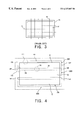
- FIG. 3 shows another conventional repair structure.
- the same method as in FIG. 1 is used to repair the line defect.
- the conventional repair structures have the following disadvantages. Since the repair line 15 is formed outside the active display region 17 in FIGS. 1, 2 and 3 , the length of the path of the repair line 15 along which the gate or data signals must flow is long. Thus, a resistance of the repair line 15 increases causing signal loss and signal delay. In addition, crosstalk at the affected area of the LCD device resulting from a parasitic capacitance generated at a crossing portion of the repair line and the gate or data line is large.
- the present invention is directed to a liquid crystal display array panel having a repair structure that substantially obviates one or more of the problems due to limitations and disadvantages of the related art.
- An object of the present invention is to provide a repair structure having a reduced or minimum length of the path in repairing opened gate or data lines.
- a liquid crystal display array panel includes a substrate; a plurality of gate lines on the substrate; a plurality of data lines on the substrate extending transverse to the plurality of gate lines; an active display region having a plurality of pixels defined by the plurality of gate lines and data lines; at least two repair lines partially positioned on the active display region and separated from each other; and wherein the repair lines cross some of the plurality of gate lines and all the data lines.
- the repair lines are in the form of a rectangular closed loop, each having first and second transverse lines spaced from each other, and first and second longitudinal lines for connecting the first and second transverse lines.
- the rectangular closed loop repair lines are spaced from and parallel to each other.
- At least one of the transverse lines of the repair line is positioned under one of the plurality of gate lines with a first insulating layer therebetween.
- the transverse line under the gate line has a protrusion in a first region under the data line other than a second region where the gate line covers.
- a liquid crystal display array panel includes a connection bar extending over corresponding longitudinal lines of the adjacent repair lines while a second insulating layer lies between the connection bar and the repair lines.
- FIG. 1 is a plan view illustrating a repair structure for an LCD device according to the prior art
- FIG. 2 shows a modified repair structure of FIG. 1
- FIG. 3 is a plan view illustrating another repair structure according to the prior art
- FIG. 4 is a plan view illustrating a repair structure according to an embodiment of the present invention.
- FIG. 5 is an enlarged view of portion “(1)” of FIG. 4;
- FIG. 6 is an enlarged view of portion “(2)” of FIG. 4;
- FIG. 7 is a sectional view taken along line VII—VII of FIG. 6;
- FIG. 8 is an enlarged view of portion “( 3 )” of FIG. 4;
- FIG. 9 is a plan view illustrating a line defect of a data line according to the embodiment of the present invention.
- FIG. 10 is a plan view illustrating a line defect of a gate line according to the embodiment of the present invention.
- an active display region 205 with a plurality of pixels is divided into three sections “A”, “B” and “C”.
- Three repair lines 301 , 303 and 305 are located in sections “A”, “B” and “C” in the form of a rectangular closed loop, respectively. They are also electrically disconnected from each other.
- the rectangular closed loop repair line 301 in section “A” has a first transverse repair line 101 , a second transverse repair line 105 spaced from and parallel to the first transverse repair line 101 , and first and second longitudinal repair lines 103 and 107 connecting the first and second transverse repair lines 101 and 105 .
- the first and second longitudinal repair lines 103 and 107 are located in the non-display region or outside the active display region 205 without overlapping the data lines (not shown).
- First and second connection bars 128 and 135 are preferably arranged to couple the rectangular closed loop repair lines 301 and 303 .
- the third and fourth connection bars 141 and 143 are also arranged to connect the rectangular closed loop repair lines 303 and 305 .
- the connection bars 128 , 135 , 141 and 143 are arranged on an insulating layer on the rectangular closed loop repair lines 301 , 303 and 305 .
- the first transverse repair line 101 is located at a portion outside the active display region 205 and crosses over the data line 203 with an insulating layer (not shown) between them.
- FIG. 6 is an enlarged view of portion ( 2 ) in FIGS. 4 .
- the transverse repair lines 105 and 109 have protrusion portions 105 a and 109 a and recess portions 105 b and 109 b , respectively, at all cross points with the data lines 203 such as the cross points “g” and “h”.
- the gate line is linearly shaped without any protrusions. Thus, there is no gate line over the protrusion portions 105 a and 109 a of the repair lines 105 and 109 .
- FIG. 7 shows a sectional view taken along line VII—VII of FIG. 6 .
- a suitable conductive metal preferably selected from the group consisting of Mo, Al, W and W-Ta or the like in order to form the repair line 109 .
- a first insulating layer 403 is formed on the repair line 109 .
- the gate line 201 On the first insulating layer 403 is formed the gate line 201 .
- a second insulating layer 405 is formed on the gate line 201 .
- the data lines 203 are formed which cross over the gate line 201 .
- the repair line 109 , the gate line 201 and the data line 203 are electrically disconnected or insulated from each other by the first and second insulating layers 403 and 405 .
- the gate line 201 When the gate line 201 become open, it is electrically connected to the repair line 109 through the first insulating layer 403 at a point where the repair line 109 is positioned below the opened gate line 201 .
- the data line 203 When the data line 203 is opened, it is shorted with the repair line 109 at the protrusion portion 109 a through the second insulating layer 405 .
- FIG. 8 shows one of the connection bars for coupling the adjacent rectangular closed loop repair lines 301 , 303 and 305 .
- the connection bar 128 couples the adjacent repair lines 301 and 303 mainly when one of the repair lines 301 and 303 is opened.
- the connection bar 128 is arranged on an insulating layer (not shown) over each end portion of the first longitudinal repair lines of the rectangular closed loop repair lines 301 and 303 .
- the rectangular closed loop repair lines 301 and 303 are connected to each other at the overlapping portions “F1” and “F2” by the connection bar 128 .
- FIG. 9 shows a method for repairing a data line with a line defect.
- the data line 203 b is connected to the first transverse repair line 109 of the closed loop repair line 303 at a cross point “K3” and to the second transverse repair line 113 of the repair line 303 at a cross point “K4”.
- the data signal can transmit through two paths P 3 and P 4 . Then, a small portion in the longer path P 4 is preferably cut.
- FIG. 10 shows a method for repairing a line defect in a gate line.
- gate lines 201 a and 201 b become open at portions OP 3 and OP 4 in section “A”, respectively.
- the gate line 201 a is connected to the first longitudinal repair line 103 of the closed loop repair line 301 at a cross point “K5” and to the second longitudinal repair line 107 of the repair line 301 at a cross point “K6”.
- the gate line 201 b is connected to the first longitudinal repair line 103 of the closed loop repair line 301 at a cross point “K7” and to the second longitudinal repair line 107 of the repair line 301 at a cross point “K8”.
- portions CP 1 and CP 2 on the first longitudinal repair line 103 and cutting portions CP 3 and CP 4 on the second longitudinal repair line 107 are removed or cut to allow each gate signal to flow separately along each corresponding path in the rectangular closed loop repair line 301 .
- the repair structure according to the present invention has several advantages. For example, since the length of the repair line becomes smaller, the resistance of the repair line decreases. Thus, signal loss and signal delay due to the open in the signal lines such as data lines and gate lines can be reduced.
- the rectangular loop repair lines shown and described in the present invention may be a closed loop as described or an open loop such as a “C” shape, for example.
Landscapes
- Physics & Mathematics (AREA)
- Nonlinear Science (AREA)
- Chemical & Material Sciences (AREA)
- Crystallography & Structural Chemistry (AREA)
- General Physics & Mathematics (AREA)
- Optics & Photonics (AREA)
- Liquid Crystal (AREA)
- Mathematical Physics (AREA)
Abstract
Description
Claims (5)
Applications Claiming Priority (2)
| Application Number | Priority Date | Filing Date | Title |
|---|---|---|---|
| KR1019980047625A KR100305322B1 (en) | 1998-11-07 | 1998-11-07 | Liquid crystal display device with repair line |
| KR98-47625 | 1998-11-07 |
Publications (1)
| Publication Number | Publication Date |
|---|---|
| US6327007B1 true US6327007B1 (en) | 2001-12-04 |
Family
ID=19557451
Family Applications (1)
| Application Number | Title | Priority Date | Filing Date |
|---|---|---|---|
| US09/434,119 Expired - Lifetime US6327007B1 (en) | 1998-11-07 | 1999-11-05 | Liquid crystal display active matrix with multiple repair lines having rectangular closed loops |
Country Status (2)
| Country | Link |
|---|---|
| US (1) | US6327007B1 (en) |
| KR (1) | KR100305322B1 (en) |
Cited By (17)
| Publication number | Priority date | Publication date | Assignee | Title |
|---|---|---|---|---|
| US20020085169A1 (en) * | 2000-12-30 | 2002-07-04 | Choi Gyo Un | Liquid crystal display for testing defects of wiring in panel |
| US6441401B1 (en) * | 1999-03-19 | 2002-08-27 | Samsung Electronics Co., Ltd. | Thin film transistor array panel for liquid crystal display and method for repairing the same |
| US20030193485A1 (en) * | 2002-04-10 | 2003-10-16 | Da Cunha John M. | Active display system |
| US6729734B2 (en) | 2002-04-01 | 2004-05-04 | Hewlett-Packard Development Company, L.P. | System for enhancing the quality of an image |
| US20050272178A1 (en) * | 2004-04-14 | 2005-12-08 | Lg.Philips Lcd Co., Ltd. | Liquid crystal display device and method for fabricating the same |
| US20080018636A1 (en) * | 2006-07-18 | 2008-01-24 | Jong-Woong Chang | Driver chip, display device and method of repair |
| US20100296018A1 (en) * | 2001-05-16 | 2010-11-25 | Dong-Gyu Kim | Thin film transistor array substrate for liquid crystal display |
| EP2256544A1 (en) | 2009-05-27 | 2010-12-01 | Polymer Vision Limited | A method for manufacturing a display panel and a display panel provided with repairable elements. |
| CN101334536B (en) * | 2007-06-28 | 2012-01-25 | 上海中航光电子有限公司 | Array substrate retain wire structure and method of manufacture |
| US20120092579A1 (en) * | 2010-10-15 | 2012-04-19 | Chunghwa Picture Tubes, Ltd. | Display device and repairing method for the same |
| WO2014026321A1 (en) * | 2012-08-13 | 2014-02-20 | 深圳市华星光电技术有限公司 | Two-dimensional display panel and repairing method thereof |
| US9006967B2 (en) | 2012-01-09 | 2015-04-14 | Samsung Display Co., Ltd. | Organic light-emitting display apparatus and method of repairing the same |
| EP2876683A3 (en) * | 2013-11-20 | 2015-06-17 | Samsung Display Co., Ltd. | Organic light emitting display apparatus and method of repairing the same |
| US9377661B2 (en) | 2011-05-23 | 2016-06-28 | Shenzhen China Star Optoelectronics Technology Co., Ltd. | Display panel and repair method thereof |
| US9460659B2 (en) | 2014-02-25 | 2016-10-04 | Samsung Display Co., Ltd. | Flexible display apparatus and method of repairing the same |
| CN106297646A (en) * | 2015-05-20 | 2017-01-04 | 上海和辉光电有限公司 | A kind of array base palte and restorative procedure thereof |
| WO2022048047A1 (en) * | 2020-09-02 | 2022-03-10 | 深圳市华星光电半导体显示技术有限公司 | Display panel and display panel manufacturing method |
Families Citing this family (2)
| Publication number | Priority date | Publication date | Assignee | Title |
|---|---|---|---|---|
| KR100719916B1 (en) * | 2000-06-28 | 2007-05-18 | 비오이 하이디스 테크놀로지 주식회사 | Thin film transistor liquid crystal display with means for line open and interlayer short repair |
| KR100906635B1 (en) * | 2002-10-23 | 2009-07-10 | 삼성전자주식회사 | Liquid crystal display |
Citations (5)
| Publication number | Priority date | Publication date | Assignee | Title |
|---|---|---|---|---|
| US5303074A (en) * | 1991-04-29 | 1994-04-12 | General Electric Company | Embedded repair lines for thin film electronic display or imager devices |
| US5608245A (en) * | 1995-12-21 | 1997-03-04 | Xerox Corporation | Array on substrate with repair line crossing lines in the array |
| US5729309A (en) * | 1995-12-05 | 1998-03-17 | Samsung Electronics Co., Ltd. | Liquid crystal display substrate having repair lines |
| US5859679A (en) * | 1996-07-11 | 1999-01-12 | Lg Electronics, Inc. | Using C-shaped repair lines and method for repairing liquid crystal display using the same |
| US6014191A (en) * | 1996-07-16 | 2000-01-11 | Samsung Electronics Co., Ltd. | Liquid crystal display having repair lines that cross data lines twice and cross gate lines in the active area and related repairing methods |
-
1998
- 1998-11-07 KR KR1019980047625A patent/KR100305322B1/en not_active Expired - Fee Related
-
1999
- 1999-11-05 US US09/434,119 patent/US6327007B1/en not_active Expired - Lifetime
Patent Citations (5)
| Publication number | Priority date | Publication date | Assignee | Title |
|---|---|---|---|---|
| US5303074A (en) * | 1991-04-29 | 1994-04-12 | General Electric Company | Embedded repair lines for thin film electronic display or imager devices |
| US5729309A (en) * | 1995-12-05 | 1998-03-17 | Samsung Electronics Co., Ltd. | Liquid crystal display substrate having repair lines |
| US5608245A (en) * | 1995-12-21 | 1997-03-04 | Xerox Corporation | Array on substrate with repair line crossing lines in the array |
| US5859679A (en) * | 1996-07-11 | 1999-01-12 | Lg Electronics, Inc. | Using C-shaped repair lines and method for repairing liquid crystal display using the same |
| US6014191A (en) * | 1996-07-16 | 2000-01-11 | Samsung Electronics Co., Ltd. | Liquid crystal display having repair lines that cross data lines twice and cross gate lines in the active area and related repairing methods |
Cited By (29)
| Publication number | Priority date | Publication date | Assignee | Title |
|---|---|---|---|---|
| US6441401B1 (en) * | 1999-03-19 | 2002-08-27 | Samsung Electronics Co., Ltd. | Thin film transistor array panel for liquid crystal display and method for repairing the same |
| US6657231B2 (en) | 1999-03-19 | 2003-12-02 | Samsung Electronics Co., Ltd. | Thin film transistor array panel |
| US20040090566A1 (en) * | 1999-03-19 | 2004-05-13 | Cheol-Soo Jung | Thin film transistor array panel |
| US7291860B2 (en) | 1999-03-19 | 2007-11-06 | Samsung Electronics Co., Ltd. | Thin film transistor array panel |
| US6999153B2 (en) * | 2000-12-30 | 2006-02-14 | Boe-Hydis Technology Co., Ltd. | Liquid crystal display for testing defects of wiring in panel |
| US20020085169A1 (en) * | 2000-12-30 | 2002-07-04 | Choi Gyo Un | Liquid crystal display for testing defects of wiring in panel |
| US8736780B2 (en) | 2001-05-16 | 2014-05-27 | Samsung Display Co., Ltd. | Thin film transistor array substrate for liquid crystal display |
| US8576346B2 (en) | 2001-05-16 | 2013-11-05 | Samsung Display Co., Ltd. | Thin film transistor array substrate for liquid crystal display |
| US20100296018A1 (en) * | 2001-05-16 | 2010-11-25 | Dong-Gyu Kim | Thin film transistor array substrate for liquid crystal display |
| US6832839B2 (en) | 2002-04-01 | 2004-12-21 | Hewlett-Packard Development Company, L.P. | System for enhancing the quality of an image |
| US6729734B2 (en) | 2002-04-01 | 2004-05-04 | Hewlett-Packard Development Company, L.P. | System for enhancing the quality of an image |
| US20040090604A1 (en) * | 2002-04-01 | 2004-05-13 | Childers Winthrop D. | System for enhancing the quality of an image |
| US20030193485A1 (en) * | 2002-04-10 | 2003-10-16 | Da Cunha John M. | Active display system |
| US7365825B2 (en) * | 2004-04-14 | 2008-04-29 | Lg.Philips Lcd Co., Ltd. | Liquid crystal display device including repair pattern and method for fabricating the same |
| US20050272178A1 (en) * | 2004-04-14 | 2005-12-08 | Lg.Philips Lcd Co., Ltd. | Liquid crystal display device and method for fabricating the same |
| US20080018636A1 (en) * | 2006-07-18 | 2008-01-24 | Jong-Woong Chang | Driver chip, display device and method of repair |
| CN101110204B (en) * | 2006-07-18 | 2013-03-27 | 三星显示有限公司 | Driver chip, display device and method of repair |
| CN101334536B (en) * | 2007-06-28 | 2012-01-25 | 上海中航光电子有限公司 | Array substrate retain wire structure and method of manufacture |
| EP2256544A1 (en) | 2009-05-27 | 2010-12-01 | Polymer Vision Limited | A method for manufacturing a display panel and a display panel provided with repairable elements. |
| US8411221B2 (en) * | 2010-10-15 | 2013-04-02 | Chunghwa Picture Tubes, Ltd. | Display device and repairing method for the same |
| US20120092579A1 (en) * | 2010-10-15 | 2012-04-19 | Chunghwa Picture Tubes, Ltd. | Display device and repairing method for the same |
| US9377661B2 (en) | 2011-05-23 | 2016-06-28 | Shenzhen China Star Optoelectronics Technology Co., Ltd. | Display panel and repair method thereof |
| US9006967B2 (en) | 2012-01-09 | 2015-04-14 | Samsung Display Co., Ltd. | Organic light-emitting display apparatus and method of repairing the same |
| WO2014026321A1 (en) * | 2012-08-13 | 2014-02-20 | 深圳市华星光电技术有限公司 | Two-dimensional display panel and repairing method thereof |
| EP2876683A3 (en) * | 2013-11-20 | 2015-06-17 | Samsung Display Co., Ltd. | Organic light emitting display apparatus and method of repairing the same |
| US9460659B2 (en) | 2014-02-25 | 2016-10-04 | Samsung Display Co., Ltd. | Flexible display apparatus and method of repairing the same |
| CN106297646A (en) * | 2015-05-20 | 2017-01-04 | 上海和辉光电有限公司 | A kind of array base palte and restorative procedure thereof |
| WO2022048047A1 (en) * | 2020-09-02 | 2022-03-10 | 深圳市华星光电半导体显示技术有限公司 | Display panel and display panel manufacturing method |
| US11852935B2 (en) | 2020-09-02 | 2023-12-26 | Shenzhen China Star Optoelectronics Semiconductor Display Technology Co., Ltd. | Display panel and method of manufacturing same |
Also Published As
| Publication number | Publication date |
|---|---|
| KR100305322B1 (en) | 2001-11-30 |
| KR20000031532A (en) | 2000-06-05 |
Similar Documents
| Publication | Publication Date | Title |
|---|---|---|
| US6327007B1 (en) | Liquid crystal display active matrix with multiple repair lines having rectangular closed loops | |
| US6111621A (en) | Flat panel display devices having improved signal line repair capability | |
| US6642972B2 (en) | Array substrate for a liquid crystal display and method for fabricating thereof with insulating stack made from TFT layers between crossed conductors | |
| US7291860B2 (en) | Thin film transistor array panel | |
| US6717634B2 (en) | Liquid crystal display and a manufacturing method thereof | |
| JP4854827B2 (en) | Thin film transistor liquid crystal display | |
| US6462800B1 (en) | Electrode contact structure for a liquid crystal display device and manufacturing method thereof | |
| US7576821B2 (en) | In-plane switching liquid crystal display device and method for fabricating the same | |
| US8289464B2 (en) | LCD device with pixels including first and second transistors of different sizes and connections | |
| US6380992B1 (en) | Liquid crystal display device having a defective pad repair structure and method for making the same | |
| US20110090446A1 (en) | Display device | |
| KR100920923B1 (en) | Array board for transverse electric field type liquid crystal display device and manufacturing method thereof | |
| KR20060079599A (en) | Array substrate and display panel having same | |
| US6118508A (en) | Liquid crystal displays including reference electrode lines that extend across multiple pixels | |
| US6642973B2 (en) | Repair structure and method for fabricating the same | |
| KR0182016B1 (en) | Thin film transistor substrate for liquid crystal display | |
| KR100653264B1 (en) | Array substrate for liquid crystal display device comprising polycrystalline silicon thin film transistor and manufacturing method thereof | |
| US5652633A (en) | Liquid crystal display device with improved crossover portion and method of forming the same | |
| US7990486B2 (en) | Liquid crystal display panel with line defect repairing mechanism and repairing method thereof | |
| JPH09288282A (en) | Liquid crystal display device and bus line disconnection processing method | |
| KR100250971B1 (en) | Planar drive type liquid crystal display device and manufacturing method thereof | |
| KR100250972B1 (en) | Liquid crystal display | |
| US7532302B2 (en) | Method of repairing gate line on TFT array substrate | |
| KR100475837B1 (en) | The substrate for LCD with a repair line and method for fabricating the same | |
| KR100921451B1 (en) | Array board for transverse electric field type liquid crystal display device and manufacturing method thereof |
Legal Events
| Date | Code | Title | Description |
|---|---|---|---|
| AS | Assignment |
Owner name: LG.PHILIPS LCD CO., LTD., KOREA, REPUBLIC OF Free format text: ASSIGNMENT OF ASSIGNORS INTEREST;ASSIGNOR:SHIM, CHANG BO;REEL/FRAME:010518/0267 Effective date: 19991231 |
|
| STCF | Information on status: patent grant |
Free format text: PATENTED CASE |
|
| FPAY | Fee payment |
Year of fee payment: 4 |
|
| AS | Assignment |
Owner name: LG DISPLAY CO., LTD., KOREA, REPUBLIC OF Free format text: CHANGE OF NAME;ASSIGNOR:LG.PHILIPS LCD CO., LTD.;REEL/FRAME:021763/0177 Effective date: 20080304 Owner name: LG DISPLAY CO., LTD.,KOREA, REPUBLIC OF Free format text: CHANGE OF NAME;ASSIGNOR:LG.PHILIPS LCD CO., LTD.;REEL/FRAME:021763/0177 Effective date: 20080304 |
|
| FPAY | Fee payment |
Year of fee payment: 8 |
|
| FEPP | Fee payment procedure |
Free format text: PAYOR NUMBER ASSIGNED (ORIGINAL EVENT CODE: ASPN); ENTITY STATUS OF PATENT OWNER: LARGE ENTITY |
|
| FPAY | Fee payment |
Year of fee payment: 12 |