US6313583B1 - Plasma processing apparatus and method - Google Patents
Plasma processing apparatus and method Download PDFInfo
- Publication number
- US6313583B1 US6313583B1 US09/450,587 US45058799A US6313583B1 US 6313583 B1 US6313583 B1 US 6313583B1 US 45058799 A US45058799 A US 45058799A US 6313583 B1 US6313583 B1 US 6313583B1
- Authority
- US
- United States
- Prior art keywords
- vacuum chamber
- plasma
- power supply
- voltage
- discharging
- Prior art date
- Legal status (The legal status is an assumption and is not a legal conclusion. Google has not performed a legal analysis and makes no representation as to the accuracy of the status listed.)
- Expired - Lifetime
Links
Images


Classifications
-
- H—ELECTRICITY
- H01—ELECTRIC ELEMENTS
- H01J—ELECTRIC DISCHARGE TUBES OR DISCHARGE LAMPS
- H01J37/00—Discharge tubes with provision for introducing objects or material to be exposed to the discharge, e.g. for the purpose of examination or processing thereof
- H01J37/32—Gas-filled discharge tubes
- H01J37/32009—Arrangements for generation of plasma specially adapted for examination or treatment of objects, e.g. plasma sources
- H01J37/32082—Radio frequency generated discharge
- H01J37/32174—Circuits specially adapted for controlling the RF discharge
-
- H—ELECTRICITY
- H01—ELECTRIC ELEMENTS
- H01J—ELECTRIC DISCHARGE TUBES OR DISCHARGE LAMPS
- H01J37/00—Discharge tubes with provision for introducing objects or material to be exposed to the discharge, e.g. for the purpose of examination or processing thereof
- H01J37/32—Gas-filled discharge tubes
- H01J37/32009—Arrangements for generation of plasma specially adapted for examination or treatment of objects, e.g. plasma sources
- H01J37/32082—Radio frequency generated discharge
Definitions
- the present invention relates to a plasma processing apparatus and method in which a plasma processing is performed for an object of processing such as a substrate.
- a plasma processing apparatus is known as an apparatus for performing a processing for cleaning of a substrate surface on which electronic parts are to be mounted.
- a plasma discharge is generated in an evacuated vacuum chamber by applying a high-frequency voltage to a discharging electrode in the vacuum chamber after the introduction of a plasma generating gas into the vacuum chamber.
- a plasma processing for an object of processing placed on the discharging electrode is performed by the action of ions, electrons or the like generated by the plasma discharge.
- a plasma processing condition such as the value of a high-frequency voltage applied to the discharging electrode should be set adequately in accordance with the object of processing.
- the setting of the plasma processing condition has been made on the basis of the result of a condition determining work performed for determining the optimum processing condition for each object of processing.
- an effective electric power representing the action of the plasma discharge for plasma generation exerted on the object of processing differs depending upon the size, thickness and material of the object of processing. Therefore, in the case where a plasma processing is performed under the same condition, it is not possible to avoid the variations in quality of the plasma processing even in the case of similar objects of processing.
- an object of the present invention is to provide a plasma processing apparatus and method in which an adequate plasma processing condition can be kept always.
- a plasma processing apparatus in which a plasma generating gas is introduced into an evacuated vacuum chamber and a high-frequency voltage is applied to a discharging electrode provided in the vacuum chamber to generate a plasma in the vacuum chamber, thereby performing a plasma processing for an object of processing placed on the discharging electrode
- the apparatus comprising a high-frequency power supply unit for applying the high-frequency voltage to the discharging electrode, a matching unit for taking the matching in impedance between the high-frequency power supply unit and a discharging circuit which produces a plasma discharge, detection means for detecting a voltage and/or current of the discharging circuit by virtue of a resistor inserted in a circuit which connects the matching unit and the discharging electrode, and control means for controlling the high-frequency power supply unit on the basis of the result of detection by the detection means.
- a plasma processing apparatus in which a plasma generating gas is introduced into an evacuated vacuum chamber and a high-frequency voltage is applied to a discharging electrode provided in the vacuum chamber to generate a plasma in the vacuum chamber, thereby performing a plasma processing for an object of processing placed on the discharging electrode
- the apparatus comprising a high-frequency power supply unit for applying the high-frequency voltage to the discharging electrode, a matching unit for taking the matching in impedance between the high-frequency power supply unit and a discharging circuit which produces a plasma discharge, detection means for detecting a voltage and/or current of the discharging circuit by virtue of a resistor inserted in a circuit which connects the matching unit and the discharging electrode, and judgement means for judging a time dependent change in internal state of the vacuum chamber through the comparison of the result of detection by the detection means with a preset reference value to give predetermined notice.
- a plasma processing method in which a plasma generating gas is introduced into a vacuum chamber after the evacuation thereof and a high-frequency voltage is applied by a high-frequency power supply unit to a discharging electrode provided in the vacuum chamber to generate a plasma in the vacuum chamber, thereby performing a plasma processing for an object of processing placed on the discharging electrode, the method comprising a step of detecting a voltage and/or current of a discharging circuit which produces a plasma discharge, the detection being made by virtue of a resistor inserted in a circuit connecting the discharging electrode and a matching unit which takes the matching in impedance between the high-frequency power supply unit and the discharging circuit, and a step of controlling the high-frequency power supply unit on the basis of the result of detection.
- a plasma processing method in which a plasma generating gas is introduced into a vacuum chamber after the evacuation thereof and a high-frequency voltage is applied by a high-frequency power supply unit to a discharging electrode provided in the vacuum chamber to generate a plasma in the vacuum chamber, thereby performing a plasma processing for an object of processing placed on the discharging electrode, the method comprising a step of detecting a voltage and/or current of a discharging circuit which produces a plasma discharge, the detection being made by virtue of a resistor inserted in a circuit connecting the discharging electrode and a matching unit which takes the matching in impedance between the high-frequency power supply unit and the discharging circuit, and a step of judging a time dependent change in internal state of the vacuum chamber through the comparison of the result of detection with a preset reference value to give predetermined notice.
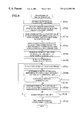
- FIG. 1 is a block diagram showing the construction of a plasma processing apparatus according to an embodiment of the present invention
- FIGS. 2 a and 2 b are cross sections of the plasma processing apparatus of the embodiment of the present invention for showing the characteristics of a plasma discharge;
- FIG. 2 c illustrates the additional capacitance generated on the inner wall of the vacuum chamber
- FIG. 3 is a flow chart showing a reference value acquisition processing in an initial state which is performed in the plasma processing apparatus of the embodiment of the present invention
- FIG. 4 is a flow chart showing a reference value acquisition processing at each time of process which is performed in the plasma processing apparatus of the embodiment of the present invention
- FIG. 5 is a flow chart showing a condition confirmation processing at the time of start which is performed in the plasma processing apparatus of the embodiment of the present invention
- FIG. 6 is a flow chart showing a processing at the time of operation which is performed in the plasma processing apparatus of the embodiment of the present invention.
- FIG. 7 shows the results of measurement of a discharge voltage by the plasma processing apparatus of the embodiment of the present invention.
- FIG. 1 a cover member 2 is provided on a base member 1 so that the cover member 2 can freely go up and down.
- a discharging electrode 4 is mounted through an insulating member 3 to the base member 1 from the lower side so that a space enclosed by the base member 1 , the discharging electrode 4 and the cover member 2 forms a vacuum chamber 5 .
- a substrate 6 made an object of plasma processing is placed on an upper surface of the discharging electrode 4 .
- the substrate 6 is different in size, thickness and material depending on the kind thereof.
- a vacuum suction unit 7 , a plasma gas supply unit 8 and an open-to-air valve 9 are connected to the cover member 2 through a pipeline.
- the vacuum suction unit 7 evacuates the air in the vacuum chamber 5 to make vacuous.
- the plasma gas supply unit 8 supplies a plasma generating gas such as an argon gas into the vacuum chamber 5 .
- the open-to-air valve 9 is opened, at the time of destruction of a vacuum state in the vacuum chamber 5 conducted after a plasma processing, so that the air is introduced into the vacuum chamber 5 .
- a high-frequency power supply unit 12 is connected to the discharging electrode 4 through a probe 10 and a matching circuit 11 .
- the matching circuit 11 is a matching unit for taking the matching in impedance between the high-frequency power supply unit 12 and a plasma discharging circuit which generates a plasma in the vacuum chamber 5 .
- the probe 10 is a resistor inserted in a circuit which connects the matching circuit 11 and the discharging electrode 4 .
- a voltage and/or current of the plasma discharging circuit can be detected by detecting a voltage between voltage detection points 14 and 15 by a monitor control unit 13 . Namely, the probe 10 and the monitor control unit 13 serve as detection means.
- An input/output control unit 16 receives the result of detection by the monitor control unit 13 and controls the matching circuit 11 and the high-frequency power supply unit 12 .
- An operation unit 20 performs an operation of making the comparison between a voltage value or current value detected by the probe 10 and the monitor control unit 13 and a reference value to determine a difference therebetween.
- a storage unit 21 stores various kinds of data necessary for operations of the plasma processing apparatus. The data includes those of plasma processing conditions (gas flow quantity pressure, discharge time, power supply output set value), such data being set for each kind of substrate by a condition determining work.
- a display unit 22 is a display monitor which displays an operation window and an input window at the time of data input and operation input by an input unit 23 and serves as notice or informing means giving various notices including an warning representative of the abnormality of the internal state of the vacuum chamber 5 .
- the input/output control unit 16 , the operation unit 20 , the storage unit 21 , the display unit 22 and the input unit 23 serve as control means for controlling the high-frequency power supply unit 12 on the basis of the detected voltage value or current value.
- FIG. 2 a illustrates the model of a plasma in the vacuum chamber 5 represented using an equivalent circuit.
- a plasma P, a sheath area S surrounding the plasma P and the substrate 6 placed on the discharging electrode 4 are replaced by a resistor R 1 , a condenser of capacitance C 1 and a condenser of capacitance C 2 , respectively.
- the capacitance C 1 of the sheath area S takes a value which is remarkably large as compared with the capacitance C 2 of the substrate 6 .
- An overall capacitance CT on the discharging electrode 4 becomes smaller as the area of the substrate 6 is increased. Under the condition that the area of the substrate 6 is fixed, CT becomes smaller as the thickness of the substrate 6 is increased and CT becomes smaller as the inductivity of the material of the substrate 6 is smaller.
- the overall capacitance CT changes with the change of the area, thickness and material of the substrate 6 as the object of processing, thereby causing a change in impedance of the equivalent circuit.
- an effective electric power for the substrate 6 at the time of plasma processing changes.
- FIG. 7 shows an example of results of measurement of such a change of the effective electric power.
- Curves a, b and c in FIG. 7 represent respective voltage values measured by use of the probe 10 in a state in which a substrate 6 made of glass epoxy resin does not exist on the discharging electrode 4 , in a state in which one substrate 6 is placed and in a state in which two substrates 6 are placed.
- a power supply output set to the same condition (500 W).
- the voltage value differs depending on the presence/absence of the substrate 6 and the number of the substrates 6 .
- the effective electric power differs even if the same power supply output condition is established. Accordingly, in order to obtain an adequate plasma processing effect, it is required that a plasma processing condition including a power supply output should be set adequately in accordance with the kind of a substrate 6 as the object of processing and the number of substrates 6 .
- FIG. 2 b shows the influence of the time dependent change of the internal state of the vacuum chamber 5 .
- the substances of the object of processing are scattered due to reverse sputtering and attach to the inner wall of the cover member 2 so that a deposited layer 2 a is formed with the lapse of time.
- the deposited layer 2 a serves as a capacitance component to generate an additional capacitance Ca (see the illustration of the circled portion of FIG. 2 b shown in FIG. 2 c ) on the inner wall of the vacuum chamber 5 which is provided in addition to the overall capacitance CT shown in FIG. 2 a .
- Ca becomes smaller as the thickness of the deposited layer 2 a is increased.
- the overall capacitance CT becomes smaller.
- Ca is infinitely large at the time of start of use of the apparatus or in an initial state in which the deposited layer 2 a does not exist.
- the impedance of the equivalent circuit changes depending on the substrate 6 as well as the growth of the deposited layer 2 a in the vacuum chamber 5 . Therefore, in order that the processing effect of the substrate as the object of processing is kept constant, the state of the deposited layer 2 a at that point of time should also be taken into consideration.
- a processing for acquiring a reference value in an initial state will be described referring to a flow chart shown in FIG. 3 .
- This processing is performed, for example, at the time of start of use of the plasma processing apparatus or after the cleaning of the interior of the vacuum chamber 5 for maintenance.
- the reference value acquisition processing is performed for acquiring a reference value representative of a condition in a state in which the internal state of the vacuum chamber 5 is satisfactory.
- a power supply output reference value P 0 is inputted from the input unit 23 to the high-frequency power supply unit 12 through the input/output control unit 16 (step ST 1 ).
- the power supply output reference value P 0 is defined for the purpose of detecting a change in impedance caused by a time dependent change in internal state of the vacuum chamber 5 irrespective of each substrate to be processed.
- the high-frequency power supply unit 12 is turned on (step ST 2 ) to detect a reference voltage V 0 by use of the probe 10 (step ST 3 ).
- the power supply output reference value P 0 and the detected reference voltage VO are stored into the storage unit 21 (step ST 4 ) and the high-frequency power supply unit 12 is turned off (step ST 5 ), thereby completing the reference value acquisition processing in the initial state.
- a processing for acquiring a reference value for each substrate to be processed (or a process reference value) will be described referring to FIG. 4 .
- a condition determining work is performed to determine or set the processing condition for each kind of substrate.
- the reference value acquisition processing is performed to a first substrate to be processed of a different kind from a just preceding one.
- a power supply output set value P 1 as an adequate power supply output has already been determined by the condition determining work for the corresponding kind of the substrate.
- a substrate 6 is arranged on the discharging electrode 4 (step ST 11 ).
- the vacuum chamber 5 is subjected to evacuation and a plasma generating gas is thereafter introduced into the vacuum chamber 5 (step ST 12 ).
- the power supply output set value P 1 is inputted from the input unit 23 to the high-frequency power supply unit 12 through the input/output control unit 16 (step ST 13 ). Then, the high-frequency power supply unit 12 is turned on (step ST 14 ) to detect a process reference voltage V 1 by use of the probe 10 (step ST 15 ). The power supply output set value P 1 and the detected process reference voltage V 1 are stored into the storage unit 21 (step ST 16 ) and the high-frequency power supply unit 12 is turned off (step ST 17 ), thereby completing the reference value acquisition processing.
- condition confirmation is made for confirming whether or not the degree of a time dependent change in internal state caused by the growth of a deposited layer on the inner wall of the vacuum chamber 5 falls within a tolerance.
- the power supply output reference value P 0 and the reference voltage V 0 indicative of the voltage value in the initial state are read from the storage unit 21 and are inputted to the operation unit 20 (step ST 21 ).
- the power supply output reference value P 0 is inputted from the operation unit 20 to the high-frequency power supply unit 12 through the input/output control unit 16 (step ST 22 ).
- the high-frequency power supply unit 12 is turned on (step ST 23 ) to detect a discharge voltage Vf by use of the probe 10 (step ST 24 ).
- the operation unit 20 determines a difference ⁇ V between the reference voltage V 0 and the discharge voltage Vf (step ST 25 ) and compares the difference ⁇ V with a threshold value ⁇ Vth (step ST 26 ). If the difference ⁇ V is not smaller than the threshold value ⁇ Vth, notice or information of a predetermined warning is outputted with the judgement of the time dependent change in internal state of the vacuum chamber 5 made as being beyond the tolerance (step ST 27 ). With this warning, a predetermined maintenance work such as the cleaning of the interior of the vacuum chamber 5 or the exchange of shielding parts is to be conducted. Namely, the operation unit 20 is judgement means for judging the time dependent change in internal state of the chamber.
- step ST 28 the time dependent change in internal state of the vacuum chamber 5 is judged as falling within the tolerance and hence the high-frequency power supply unit 12 is immediately turned off (step ST 28 ), thereby completing the condition confirmation processing at the time of start.
- a processing at the time of operation of the plasma processing apparatus will be described referring to FIG. 6 .
- This processing is performed for ensuring an adequate plasma processing condition at the time of actual plasma processing.
- a substrate 6 is arranged on the discharging electrode 4 (step ST 31 ).
- the vacuum chamber 5 is subjected to evacuation and a plasma generating gas is thereafter introduced into the vacuum chamber 5 (step ST 32 ).
- a power supply output set value P 1 corresponding to the substrate 6 to be processed and the process reference voltage V 1 determined by the process reference value acquisition processing are read from the storage unit 21 and are inputted to the operation unit 20 (step ST 33 ).
- the power supply output set value P 1 is inputted from the operation unit 20 to the high-frequency power supply unit 12 through the input/output control unit 16 (step ST 34 ).
- a discharging time t is read from the storage unit 21 , which time t was determined by the condition determining work and stored, and is inputted to the input/output control unit 16 (step ST 35 ) and the high-frequency power supply unit 12 is turned on (step ST 36 ).
- a discharge voltage Vs is detected by the probe 10 (step ST 37 ).
- the operation unit 20 determines a difference ⁇ V between the process reference voltage V 1 and the detected discharge voltage Vs (step ST 38 ) and compares the determined difference ⁇ V with a preset value ⁇ V 1 (step ST 39 ).
- the preset value ⁇ V 1 is set on the basis of the tolerable range of variations of the plasma processing effect. If the difference ⁇ V is smaller than a preset value ⁇ V 1 , that is, if the discharge voltage Vs falls in a predetermined preset range it is determined that the plasma processing effect falls in a tolerance, the plasma processing is continued until it is confirmed that the preset discharging time t is up (step ST 41 ).
- step ST 39 if it is determined in step ST 39 that the difference ⁇ V is not smaller than the preset value ⁇ V 1 , it is meant that the discharge voltage Vs is out of a proper voltage.
- the power supply output set value P 1 at the present point of time is changed by adding a predetermined value A thereto and the changed value P 1 is newly inputted to the high-frequency power supply unit 12 (step ST 40 ) and the flow returns to step ST 37 to detect the discharge voltage Vs again.
- the processings up to step ST 40 are repeated.
- the high-frequency power supply unit 12 is turned off (step ST 42 ), thereby completing the plasma processing.
- a discharge voltage is detected at each time of operation of the plasma processing apparatus in order that an effective electric power for an object of processing at the time of plasma processing is kept constant.
- a necessary feedback is made for the high-frequency power supply unit.
- the detection is made by inserting the resistor between the discharging electrode 4 and the matching circuit 11 .
- the method according to the present embodiment requires only the detection of a voltage or current. In the present embodiment, it is therefore possible to shorten a detecting/processing time and to simplify the measuring/operating function, thereby reducing the installation or equipment cost. Also, with the detection of the voltage between the discharging electrode 4 and the matching circuit 11 , an influence which the change of the substrate 6 to be processed gives on a value to be detected can be measured with a high sensitivity. Therefore, the stability of sensitivity is superior as compared with the conventional method in which a sensor is installed in the vacuum chamber 5 .
- a reference value for a voltage when no deposited layer exists in the vacuum chamber 5 is determined so that it is sure at the time of start to compare a detected value with the reference value. Thereby, it is possible to accurately give notice of a timing for a maintenance work for the vacuum chamber 5 . As a result, it is possible to reduce a load imposed for maintenance and/or management.
- a voltage is determined as the reference value or the value to be detected.
- a current may be determined in lieu of the voltage.
- a voltage or current of a discharging circuit is detected by a resistor inserted in a circuit connecting a matching unit and a discharging electrode and a high-frequency power supply is controlled on the basis of the result of detection.
- the result of detection is compared with a reference value in an initial state. Thereby, it is possible to properly estimate a time dependent change in internal state of a vacuum chamber. As a result, it is possible to adequately judge whether or not the maintenance is required.
Landscapes
- Physics & Mathematics (AREA)
- Engineering & Computer Science (AREA)
- Plasma & Fusion (AREA)
- Chemical & Material Sciences (AREA)
- Analytical Chemistry (AREA)
- Plasma Technology (AREA)
- Physical Vapour Deposition (AREA)
- Drying Of Semiconductors (AREA)
Abstract
Description
Claims (15)
Applications Claiming Priority (2)
| Application Number | Priority Date | Filing Date | Title |
|---|---|---|---|
| JP10341243A JP2000173982A (en) | 1998-12-01 | 1998-12-01 | Plasma processing apparatus and plasma processing method |
| JP10-341243 | 1998-12-01 |
Publications (1)
| Publication Number | Publication Date |
|---|---|
| US6313583B1 true US6313583B1 (en) | 2001-11-06 |
Family
ID=18344517
Family Applications (1)
| Application Number | Title | Priority Date | Filing Date |
|---|---|---|---|
| US09/450,587 Expired - Lifetime US6313583B1 (en) | 1998-12-01 | 1999-11-30 | Plasma processing apparatus and method |
Country Status (2)
| Country | Link |
|---|---|
| US (1) | US6313583B1 (en) |
| JP (1) | JP2000173982A (en) |
Cited By (66)
| Publication number | Priority date | Publication date | Assignee | Title |
|---|---|---|---|---|
| US6456010B2 (en) * | 2000-03-13 | 2002-09-24 | Mitsubishi Heavy Industries, Ltd. | Discharge plasma generating method, discharge plasma generating apparatus, semiconductor device fabrication method, and semiconductor device fabrication apparatus |
| US6476378B2 (en) * | 1999-12-27 | 2002-11-05 | Sony Corporation | Imaging apparatus and method of same |
| US6538388B2 (en) * | 2000-10-16 | 2003-03-25 | Alps Electric Co., Ltd. | Plasma processing apparatus suitable for power supply of higher frequency |
| US6551444B2 (en) | 2001-04-12 | 2003-04-22 | Matsushita Electric Industrial Co., Ltd. | Plasma processing apparatus and method of processing |
| US6772776B2 (en) * | 2001-09-18 | 2004-08-10 | Euv Llc | Apparatus for in situ cleaning of carbon contaminated surfaces |
| US20050000440A1 (en) * | 2000-11-08 | 2005-01-06 | Akira Nakano | Plasma processing apparatus including a plurality of plasma processing units having reduced variation |
| US20050061442A1 (en) * | 2001-12-13 | 2005-03-24 | Tsutomu Higashiura | Plasma treatment apparatus and control method thereof |
| WO2007052902A1 (en) * | 2005-11-04 | 2007-05-10 | Korea Research Institute Of Standards And Science | Plasma diagnostic apparatus and method |
| US20070200658A1 (en) * | 2006-01-06 | 2007-08-30 | Samsung Electronics Co., Ltd. | Apparatus and method for transmitting control commands in home network system |
| US20070227876A1 (en) * | 2006-03-29 | 2007-10-04 | Applied Materials, Inc. | RF powered target for increasing deposition uniformity in sputtering systems |
| US20080265903A1 (en) * | 2005-11-04 | 2008-10-30 | Chin-Wook Chung | Plasma Diagnostic Apparatus And Method |
| US20090224874A1 (en) * | 2008-03-05 | 2009-09-10 | International Business Machines Corporation | Apparatus, system, and method for providing authentication and activation functions to a computing device |
| US20100276273A1 (en) * | 2009-05-01 | 2010-11-04 | Advanced Energy Industries, Inc. | Method and apparatus for controlling ion energy distribution |
| CN101971713A (en) * | 2008-03-13 | 2011-02-09 | 应用材料公司 | Electrical control of plasma uniformity using external circuit |
| US20110295554A1 (en) * | 2010-05-26 | 2011-12-01 | Samsung Electronics Co., Ltd. | Equipment For Manufacturing Semiconductor Device And Seasoning Process Method Of The Same |
| EP1976347A3 (en) * | 2007-03-30 | 2012-01-11 | Tokyo Electron Limited | Plasma processing apparatus, radio frequency generator and correction method therefor |
| WO2014035889A1 (en) * | 2012-08-28 | 2014-03-06 | Advanced Energy Industries, Inc. | Systems and methods for monitoring faults, anomalies, and other characteristics of a switched mode ion energy distribution system |
| JP2015065378A (en) * | 2013-09-26 | 2015-04-09 | 芝浦メカトロニクス株式会社 | Plasma processing apparatus and plasma processing method |
| US9105447B2 (en) | 2012-08-28 | 2015-08-11 | Advanced Energy Industries, Inc. | Wide dynamic range ion energy bias control; fast ion energy switching; ion energy control and a pulsed bias supply; and a virtual front panel |
| US9208992B2 (en) | 2010-04-26 | 2015-12-08 | Advanced Energy Industries, Inc. | Method for controlling ion energy distribution |
| US9210790B2 (en) | 2012-08-28 | 2015-12-08 | Advanced Energy Industries, Inc. | Systems and methods for calibrating a switched mode ion energy distribution system |
| US9309594B2 (en) | 2010-04-26 | 2016-04-12 | Advanced Energy Industries, Inc. | System, method and apparatus for controlling ion energy distribution of a projected plasma |
| US9362089B2 (en) | 2010-08-29 | 2016-06-07 | Advanced Energy Industries, Inc. | Method of controlling the switched mode ion energy distribution system |
| US9435029B2 (en) | 2010-08-29 | 2016-09-06 | Advanced Energy Industries, Inc. | Wafer chucking system for advanced plasma ion energy processing systems |
| US9767988B2 (en) | 2010-08-29 | 2017-09-19 | Advanced Energy Industries, Inc. | Method of controlling the switched mode ion energy distribution system |
| CN108257842A (en) * | 2016-12-27 | 2018-07-06 | 株式会社日立国际电气 | The manufacturing method and recording medium of substrate processing device, semiconductor devices |
| US10607813B2 (en) | 2017-11-17 | 2020-03-31 | Advanced Energy Industries, Inc. | Synchronized pulsing of plasma processing source and substrate bias |
| US20200154556A1 (en) * | 2018-05-10 | 2020-05-14 | Applied Materials, Inc. | Method of controlling ion energy distribution using a pulse generator with a current-return output stage |
| US10707055B2 (en) | 2017-11-17 | 2020-07-07 | Advanced Energy Industries, Inc. | Spatial and temporal control of ion bias voltage for plasma processing |
| US10811229B2 (en) | 2017-11-17 | 2020-10-20 | Advanced Energy Industries, Inc. | Synchronization with a bias supply in a plasma processing system |
| CN112534561A (en) * | 2018-08-02 | 2021-03-19 | 朗姆研究公司 | Compensating for chamber and process effects to improve CD variation of a trim process |
| US11462389B2 (en) | 2020-07-31 | 2022-10-04 | Applied Materials, Inc. | Pulsed-voltage hardware assembly for use in a plasma processing system |
| US11476090B1 (en) | 2021-08-24 | 2022-10-18 | Applied Materials, Inc. | Voltage pulse time-domain multiplexing |
| US11476145B2 (en) | 2018-11-20 | 2022-10-18 | Applied Materials, Inc. | Automatic ESC bias compensation when using pulsed DC bias |
| US11495470B1 (en) | 2021-04-16 | 2022-11-08 | Applied Materials, Inc. | Method of enhancing etching selectivity using a pulsed plasma |
| US11508554B2 (en) | 2019-01-24 | 2022-11-22 | Applied Materials, Inc. | High voltage filter assembly |
| US11569066B2 (en) | 2021-06-23 | 2023-01-31 | Applied Materials, Inc. | Pulsed voltage source for plasma processing applications |
| US11615941B2 (en) | 2009-05-01 | 2023-03-28 | Advanced Energy Industries, Inc. | System, method, and apparatus for controlling ion energy distribution in plasma processing systems |
| US11670487B1 (en) | 2022-01-26 | 2023-06-06 | Advanced Energy Industries, Inc. | Bias supply control and data processing |
| US11694876B2 (en) | 2021-12-08 | 2023-07-04 | Applied Materials, Inc. | Apparatus and method for delivering a plurality of waveform signals during plasma processing |
| US11699572B2 (en) | 2019-01-22 | 2023-07-11 | Applied Materials, Inc. | Feedback loop for controlling a pulsed voltage waveform |
| US11776788B2 (en) | 2021-06-28 | 2023-10-03 | Applied Materials, Inc. | Pulsed voltage boost for substrate processing |
| US11791138B2 (en) | 2021-05-12 | 2023-10-17 | Applied Materials, Inc. | Automatic electrostatic chuck bias compensation during plasma processing |
| US11798790B2 (en) | 2020-11-16 | 2023-10-24 | Applied Materials, Inc. | Apparatus and methods for controlling ion energy distribution |
| US11810760B2 (en) | 2021-06-16 | 2023-11-07 | Applied Materials, Inc. | Apparatus and method of ion current compensation |
| US11887812B2 (en) | 2019-07-12 | 2024-01-30 | Advanced Energy Industries, Inc. | Bias supply with a single controlled switch |
| US11901157B2 (en) | 2020-11-16 | 2024-02-13 | Applied Materials, Inc. | Apparatus and methods for controlling ion energy distribution |
| US11942309B2 (en) | 2022-01-26 | 2024-03-26 | Advanced Energy Industries, Inc. | Bias supply with resonant switching |
| US11948780B2 (en) | 2021-05-12 | 2024-04-02 | Applied Materials, Inc. | Automatic electrostatic chuck bias compensation during plasma processing |
| US11967483B2 (en) | 2021-06-02 | 2024-04-23 | Applied Materials, Inc. | Plasma excitation with ion energy control |
| US11972924B2 (en) | 2022-06-08 | 2024-04-30 | Applied Materials, Inc. | Pulsed voltage source for plasma processing applications |
| US11978613B2 (en) | 2022-09-01 | 2024-05-07 | Advanced Energy Industries, Inc. | Transition control in a bias supply |
| US11984306B2 (en) | 2021-06-09 | 2024-05-14 | Applied Materials, Inc. | Plasma chamber and chamber component cleaning methods |
| US20240242944A1 (en) * | 2023-01-18 | 2024-07-18 | Samsung Electronics Co., Ltd. | Plasma diagnostic apparatus and operating method thereof |
| US12046448B2 (en) | 2022-01-26 | 2024-07-23 | Advanced Energy Industries, Inc. | Active switch on time control for bias supply |
| US12106938B2 (en) | 2021-09-14 | 2024-10-01 | Applied Materials, Inc. | Distortion current mitigation in a radio frequency plasma processing chamber |
| US12111341B2 (en) | 2022-10-05 | 2024-10-08 | Applied Materials, Inc. | In-situ electric field detection method and apparatus |
| US12125674B2 (en) | 2020-05-11 | 2024-10-22 | Advanced Energy Industries, Inc. | Surface charge and power feedback and control using a switch mode bias system |
| US12148595B2 (en) | 2021-06-09 | 2024-11-19 | Applied Materials, Inc. | Plasma uniformity control in pulsed DC plasma chamber |
| US12159767B2 (en) | 2017-11-17 | 2024-12-03 | Advanced Energy Industries, Inc. | Spatial control of plasma processing environments |
| US12198966B2 (en) | 2017-09-20 | 2025-01-14 | Applied Materials, Inc. | Substrate support with multiple embedded electrodes |
| US12230476B2 (en) | 2017-11-17 | 2025-02-18 | Advanced Energy Industries, Inc. | Integrated control of a plasma processing system |
| US12272524B2 (en) | 2022-09-19 | 2025-04-08 | Applied Materials, Inc. | Wideband variable impedance load for high volume manufacturing qualification and on-site diagnostics |
| US12315732B2 (en) | 2022-06-10 | 2025-05-27 | Applied Materials, Inc. | Method and apparatus for etching a semiconductor substrate in a plasma etch chamber |
| US12505986B2 (en) | 2017-11-17 | 2025-12-23 | Advanced Energy Industries, Inc. | Synchronization of plasma processing components |
| US12525433B2 (en) | 2021-06-09 | 2026-01-13 | Applied Materials, Inc. | Method and apparatus to reduce feature charging in plasma processing chamber |
Families Citing this family (7)
| Publication number | Priority date | Publication date | Assignee | Title |
|---|---|---|---|---|
| JP3600144B2 (en) * | 2000-09-22 | 2004-12-08 | アルプス電気株式会社 | Performance evaluation method, maintenance method, and performance management system for plasma processing apparatus, and plasma processing apparatus and performance confirmation system for plasma processing apparatus |
| JP3670206B2 (en) * | 2000-11-06 | 2005-07-13 | アルプス電気株式会社 | Performance evaluation method, maintenance method, performance management system, performance confirmation system, and plasma processing apparatus for plasma processing apparatus or plasma processing system |
| JP3923323B2 (en) * | 2002-01-30 | 2007-05-30 | アルプス電気株式会社 | Plasma processing apparatus and plasma processing method |
| JP4186536B2 (en) | 2002-07-18 | 2008-11-26 | 松下電器産業株式会社 | Plasma processing equipment |
| JP5255907B2 (en) * | 2008-05-26 | 2013-08-07 | ラピスセミコンダクタ株式会社 | Plasma monitoring system |
| CN105206494B (en) * | 2014-06-18 | 2017-06-06 | 北京北方微电子基地设备工艺研究中心有限责任公司 | The impedance matching methods of pulse radiation frequency power supply and the matching process of plasma apparatus |
| JP6806883B2 (en) * | 2017-04-04 | 2021-01-06 | 株式会社Fuji | Information processing device |
Citations (7)
| Publication number | Priority date | Publication date | Assignee | Title |
|---|---|---|---|---|
| US4970435A (en) * | 1987-12-09 | 1990-11-13 | Tel Sagami Limited | Plasma processing apparatus |
| US5543689A (en) * | 1993-12-27 | 1996-08-06 | Fujitsu Limited | High frequency power source having corrected power output |
| JPH0992491A (en) | 1995-09-28 | 1997-04-04 | Toshiba Corp | Plasma processing apparatus and plasma processing method |
| US5708250A (en) * | 1996-03-29 | 1998-01-13 | Lam Resarch Corporation | Voltage controller for electrostatic chuck of vacuum plasma processors |
| JPH10125494A (en) | 1996-10-25 | 1998-05-15 | Toshiba Corp | Plasma processing apparatus and plasma processing method |
| US5916455A (en) * | 1996-03-18 | 1999-06-29 | Applied Materials, Inc. | Method and apparatus for generating a low pressure plasma |
| US6031198A (en) * | 1997-05-22 | 2000-02-29 | Canon Kabushiki Kaisha | Plasma processing method and apparatus |
-
1998
- 1998-12-01 JP JP10341243A patent/JP2000173982A/en active Pending
-
1999
- 1999-11-30 US US09/450,587 patent/US6313583B1/en not_active Expired - Lifetime
Patent Citations (7)
| Publication number | Priority date | Publication date | Assignee | Title |
|---|---|---|---|---|
| US4970435A (en) * | 1987-12-09 | 1990-11-13 | Tel Sagami Limited | Plasma processing apparatus |
| US5543689A (en) * | 1993-12-27 | 1996-08-06 | Fujitsu Limited | High frequency power source having corrected power output |
| JPH0992491A (en) | 1995-09-28 | 1997-04-04 | Toshiba Corp | Plasma processing apparatus and plasma processing method |
| US5916455A (en) * | 1996-03-18 | 1999-06-29 | Applied Materials, Inc. | Method and apparatus for generating a low pressure plasma |
| US5708250A (en) * | 1996-03-29 | 1998-01-13 | Lam Resarch Corporation | Voltage controller for electrostatic chuck of vacuum plasma processors |
| JPH10125494A (en) | 1996-10-25 | 1998-05-15 | Toshiba Corp | Plasma processing apparatus and plasma processing method |
| US6031198A (en) * | 1997-05-22 | 2000-02-29 | Canon Kabushiki Kaisha | Plasma processing method and apparatus |
Cited By (101)
| Publication number | Priority date | Publication date | Assignee | Title |
|---|---|---|---|---|
| US6476378B2 (en) * | 1999-12-27 | 2002-11-05 | Sony Corporation | Imaging apparatus and method of same |
| US6456010B2 (en) * | 2000-03-13 | 2002-09-24 | Mitsubishi Heavy Industries, Ltd. | Discharge plasma generating method, discharge plasma generating apparatus, semiconductor device fabrication method, and semiconductor device fabrication apparatus |
| US6538388B2 (en) * | 2000-10-16 | 2003-03-25 | Alps Electric Co., Ltd. | Plasma processing apparatus suitable for power supply of higher frequency |
| US20050000440A1 (en) * | 2000-11-08 | 2005-01-06 | Akira Nakano | Plasma processing apparatus including a plurality of plasma processing units having reduced variation |
| US7225754B2 (en) * | 2000-11-08 | 2007-06-05 | Alps Electric Co., Ltd. | Plasma processing apparatus including a plurality of plasma processing units having reduced variation |
| US6551444B2 (en) | 2001-04-12 | 2003-04-22 | Matsushita Electric Industrial Co., Ltd. | Plasma processing apparatus and method of processing |
| US6772776B2 (en) * | 2001-09-18 | 2004-08-10 | Euv Llc | Apparatus for in situ cleaning of carbon contaminated surfaces |
| US7244475B2 (en) * | 2001-12-13 | 2007-07-17 | Tokyo Electron Limited | Plasma treatment apparatus and control method thereof |
| US20050061442A1 (en) * | 2001-12-13 | 2005-03-24 | Tsutomu Higashiura | Plasma treatment apparatus and control method thereof |
| US20080265903A1 (en) * | 2005-11-04 | 2008-10-30 | Chin-Wook Chung | Plasma Diagnostic Apparatus And Method |
| US7696758B2 (en) | 2005-11-04 | 2010-04-13 | Korea Research Institute Of Standards And Science | Plasma diagnostic apparatus and method |
| WO2007052902A1 (en) * | 2005-11-04 | 2007-05-10 | Korea Research Institute Of Standards And Science | Plasma diagnostic apparatus and method |
| US20070200658A1 (en) * | 2006-01-06 | 2007-08-30 | Samsung Electronics Co., Ltd. | Apparatus and method for transmitting control commands in home network system |
| US20070227876A1 (en) * | 2006-03-29 | 2007-10-04 | Applied Materials, Inc. | RF powered target for increasing deposition uniformity in sputtering systems |
| US7517437B2 (en) * | 2006-03-29 | 2009-04-14 | Applied Materials, Inc. | RF powered target for increasing deposition uniformity in sputtering systems |
| EP1976347A3 (en) * | 2007-03-30 | 2012-01-11 | Tokyo Electron Limited | Plasma processing apparatus, radio frequency generator and correction method therefor |
| US20090224874A1 (en) * | 2008-03-05 | 2009-09-10 | International Business Machines Corporation | Apparatus, system, and method for providing authentication and activation functions to a computing device |
| CN101971713A (en) * | 2008-03-13 | 2011-02-09 | 应用材料公司 | Electrical control of plasma uniformity using external circuit |
| US11011349B2 (en) | 2009-05-01 | 2021-05-18 | Aes Global Holdings, Pte. Ltd. | System, method, and apparatus for controlling ion energy distribution in plasma processing systems |
| US11615941B2 (en) | 2009-05-01 | 2023-03-28 | Advanced Energy Industries, Inc. | System, method, and apparatus for controlling ion energy distribution in plasma processing systems |
| US20100276273A1 (en) * | 2009-05-01 | 2010-11-04 | Advanced Energy Industries, Inc. | Method and apparatus for controlling ion energy distribution |
| US9287092B2 (en) | 2009-05-01 | 2016-03-15 | Advanced Energy Industries, Inc. | Method and apparatus for controlling ion energy distribution |
| US9287086B2 (en) | 2010-04-26 | 2016-03-15 | Advanced Energy Industries, Inc. | System, method and apparatus for controlling ion energy distribution |
| US9208992B2 (en) | 2010-04-26 | 2015-12-08 | Advanced Energy Industries, Inc. | Method for controlling ion energy distribution |
| US9309594B2 (en) | 2010-04-26 | 2016-04-12 | Advanced Energy Industries, Inc. | System, method and apparatus for controlling ion energy distribution of a projected plasma |
| US20110295554A1 (en) * | 2010-05-26 | 2011-12-01 | Samsung Electronics Co., Ltd. | Equipment For Manufacturing Semiconductor Device And Seasoning Process Method Of The Same |
| US9136138B2 (en) * | 2010-05-26 | 2015-09-15 | Samsung Electronics Co., Ltd. | Equipment for manufacturing semiconductor device and seasoning process method of the same |
| US9435029B2 (en) | 2010-08-29 | 2016-09-06 | Advanced Energy Industries, Inc. | Wafer chucking system for advanced plasma ion energy processing systems |
| US9767988B2 (en) | 2010-08-29 | 2017-09-19 | Advanced Energy Industries, Inc. | Method of controlling the switched mode ion energy distribution system |
| US9362089B2 (en) | 2010-08-29 | 2016-06-07 | Advanced Energy Industries, Inc. | Method of controlling the switched mode ion energy distribution system |
| US9105447B2 (en) | 2012-08-28 | 2015-08-11 | Advanced Energy Industries, Inc. | Wide dynamic range ion energy bias control; fast ion energy switching; ion energy control and a pulsed bias supply; and a virtual front panel |
| US9685297B2 (en) | 2012-08-28 | 2017-06-20 | Advanced Energy Industries, Inc. | Systems and methods for monitoring faults, anomalies, and other characteristics of a switched mode ion energy distribution system |
| US11189454B2 (en) | 2012-08-28 | 2021-11-30 | Aes Global Holdings, Pte. Ltd. | Systems and methods for monitoring faults, anomalies, and other characteristics of a switched mode ion energy distribution system |
| US9210790B2 (en) | 2012-08-28 | 2015-12-08 | Advanced Energy Industries, Inc. | Systems and methods for calibrating a switched mode ion energy distribution system |
| US12142452B2 (en) | 2012-08-28 | 2024-11-12 | Advanced Energy Industries, Inc. | Systems and methods for monitoring faults, anomalies, and other characteristics of a switched mode ion energy distribution system |
| WO2014035889A1 (en) * | 2012-08-28 | 2014-03-06 | Advanced Energy Industries, Inc. | Systems and methods for monitoring faults, anomalies, and other characteristics of a switched mode ion energy distribution system |
| TWI560738B (en) * | 2012-08-28 | 2016-12-01 | Advanced Energy Ind Inc | Systems and methods for monitoring faults, anomalies, and other characteristics of a switched mode ion energy distribution system |
| JP2015065378A (en) * | 2013-09-26 | 2015-04-09 | 芝浦メカトロニクス株式会社 | Plasma processing apparatus and plasma processing method |
| CN108257842B (en) * | 2016-12-27 | 2020-07-14 | 株式会社国际电气 | Substrate processing apparatus, method of manufacturing semiconductor device, and recording medium |
| CN108257842A (en) * | 2016-12-27 | 2018-07-06 | 株式会社日立国际电气 | The manufacturing method and recording medium of substrate processing device, semiconductor devices |
| US10679831B2 (en) | 2016-12-27 | 2020-06-09 | Kokusia Electric Corporation | Substrate processing apparatus, method of manufacturing semiconductor device and non-transitory computer-readable recording medium |
| US12198966B2 (en) | 2017-09-20 | 2025-01-14 | Applied Materials, Inc. | Substrate support with multiple embedded electrodes |
| US10811229B2 (en) | 2017-11-17 | 2020-10-20 | Advanced Energy Industries, Inc. | Synchronization with a bias supply in a plasma processing system |
| US10811227B2 (en) | 2017-11-17 | 2020-10-20 | Advanced Energy Industries, Inc. | Application of modulating supplies in a plasma processing system |
| US10896807B2 (en) | 2017-11-17 | 2021-01-19 | Advanced Energy Industries, Inc. | Synchronization between an excitation source and a substrate bias supply |
| US10811228B2 (en) | 2017-11-17 | 2020-10-20 | Advanced Energy Industries, Inc. | Control of plasma processing systems that include plasma modulating supplies |
| US10707055B2 (en) | 2017-11-17 | 2020-07-07 | Advanced Energy Industries, Inc. | Spatial and temporal control of ion bias voltage for plasma processing |
| US10607813B2 (en) | 2017-11-17 | 2020-03-31 | Advanced Energy Industries, Inc. | Synchronized pulsing of plasma processing source and substrate bias |
| US12159767B2 (en) | 2017-11-17 | 2024-12-03 | Advanced Energy Industries, Inc. | Spatial control of plasma processing environments |
| US12505986B2 (en) | 2017-11-17 | 2025-12-23 | Advanced Energy Industries, Inc. | Synchronization of plasma processing components |
| US11842884B2 (en) | 2017-11-17 | 2023-12-12 | Advanced Energy Industries, Inc. | Spatial monitoring and control of plasma processing environments |
| US12230476B2 (en) | 2017-11-17 | 2025-02-18 | Advanced Energy Industries, Inc. | Integrated control of a plasma processing system |
| US20200154556A1 (en) * | 2018-05-10 | 2020-05-14 | Applied Materials, Inc. | Method of controlling ion energy distribution using a pulse generator with a current-return output stage |
| US11284500B2 (en) | 2018-05-10 | 2022-03-22 | Applied Materials, Inc. | Method of controlling ion energy distribution using a pulse generator |
| US10791617B2 (en) * | 2018-05-10 | 2020-09-29 | Applied Materials, Inc. | Method of controlling ion energy distribution using a pulse generator with a current-return output stage |
| CN112534561A (en) * | 2018-08-02 | 2021-03-19 | 朗姆研究公司 | Compensating for chamber and process effects to improve CD variation of a trim process |
| US11476145B2 (en) | 2018-11-20 | 2022-10-18 | Applied Materials, Inc. | Automatic ESC bias compensation when using pulsed DC bias |
| US11699572B2 (en) | 2019-01-22 | 2023-07-11 | Applied Materials, Inc. | Feedback loop for controlling a pulsed voltage waveform |
| US12057292B2 (en) | 2019-01-22 | 2024-08-06 | Applied Materials, Inc. | Feedback loop for controlling a pulsed voltage waveform |
| US11508554B2 (en) | 2019-01-24 | 2022-11-22 | Applied Materials, Inc. | High voltage filter assembly |
| US11887812B2 (en) | 2019-07-12 | 2024-01-30 | Advanced Energy Industries, Inc. | Bias supply with a single controlled switch |
| US12125674B2 (en) | 2020-05-11 | 2024-10-22 | Advanced Energy Industries, Inc. | Surface charge and power feedback and control using a switch mode bias system |
| US11462388B2 (en) | 2020-07-31 | 2022-10-04 | Applied Materials, Inc. | Plasma processing assembly using pulsed-voltage and radio-frequency power |
| US11848176B2 (en) | 2020-07-31 | 2023-12-19 | Applied Materials, Inc. | Plasma processing using pulsed-voltage and radio-frequency power |
| US11776789B2 (en) | 2020-07-31 | 2023-10-03 | Applied Materials, Inc. | Plasma processing assembly using pulsed-voltage and radio-frequency power |
| US12237148B2 (en) | 2020-07-31 | 2025-02-25 | Applied Materials, Inc. | Plasma processing assembly using pulsed-voltage and radio-frequency power |
| US11462389B2 (en) | 2020-07-31 | 2022-10-04 | Applied Materials, Inc. | Pulsed-voltage hardware assembly for use in a plasma processing system |
| US11798790B2 (en) | 2020-11-16 | 2023-10-24 | Applied Materials, Inc. | Apparatus and methods for controlling ion energy distribution |
| US12183557B2 (en) | 2020-11-16 | 2024-12-31 | Applied Materials, Inc. | Apparatus and methods for controlling ion energy distribution |
| US11901157B2 (en) | 2020-11-16 | 2024-02-13 | Applied Materials, Inc. | Apparatus and methods for controlling ion energy distribution |
| US11495470B1 (en) | 2021-04-16 | 2022-11-08 | Applied Materials, Inc. | Method of enhancing etching selectivity using a pulsed plasma |
| US11948780B2 (en) | 2021-05-12 | 2024-04-02 | Applied Materials, Inc. | Automatic electrostatic chuck bias compensation during plasma processing |
| US11791138B2 (en) | 2021-05-12 | 2023-10-17 | Applied Materials, Inc. | Automatic electrostatic chuck bias compensation during plasma processing |
| US11967483B2 (en) | 2021-06-02 | 2024-04-23 | Applied Materials, Inc. | Plasma excitation with ion energy control |
| US12347647B2 (en) | 2021-06-02 | 2025-07-01 | Applied Materials, Inc. | Plasma excitation with ion energy control |
| US12525433B2 (en) | 2021-06-09 | 2026-01-13 | Applied Materials, Inc. | Method and apparatus to reduce feature charging in plasma processing chamber |
| US12394596B2 (en) | 2021-06-09 | 2025-08-19 | Applied Materials, Inc. | Plasma uniformity control in pulsed DC plasma chamber |
| US11984306B2 (en) | 2021-06-09 | 2024-05-14 | Applied Materials, Inc. | Plasma chamber and chamber component cleaning methods |
| US12525441B2 (en) | 2021-06-09 | 2026-01-13 | Applied Materials, Inc. | Plasma chamber and chamber component cleaning methods |
| US12148595B2 (en) | 2021-06-09 | 2024-11-19 | Applied Materials, Inc. | Plasma uniformity control in pulsed DC plasma chamber |
| US11810760B2 (en) | 2021-06-16 | 2023-11-07 | Applied Materials, Inc. | Apparatus and method of ion current compensation |
| US12125673B2 (en) | 2021-06-23 | 2024-10-22 | Applied Materials, Inc. | Pulsed voltage source for plasma processing applications |
| US11887813B2 (en) | 2021-06-23 | 2024-01-30 | Applied Materials, Inc. | Pulsed voltage source for plasma processing |
| US11569066B2 (en) | 2021-06-23 | 2023-01-31 | Applied Materials, Inc. | Pulsed voltage source for plasma processing applications |
| US11776788B2 (en) | 2021-06-28 | 2023-10-03 | Applied Materials, Inc. | Pulsed voltage boost for substrate processing |
| US12261019B2 (en) | 2021-08-24 | 2025-03-25 | Applied Materials, Inc. | Voltage pulse time-domain multiplexing |
| US11476090B1 (en) | 2021-08-24 | 2022-10-18 | Applied Materials, Inc. | Voltage pulse time-domain multiplexing |
| US12106938B2 (en) | 2021-09-14 | 2024-10-01 | Applied Materials, Inc. | Distortion current mitigation in a radio frequency plasma processing chamber |
| US12482633B2 (en) | 2021-12-08 | 2025-11-25 | Applied Materials, Inc. | Apparatus and method for delivering a plurality of waveform signals during plasma processing |
| US11694876B2 (en) | 2021-12-08 | 2023-07-04 | Applied Materials, Inc. | Apparatus and method for delivering a plurality of waveform signals during plasma processing |
| US12046448B2 (en) | 2022-01-26 | 2024-07-23 | Advanced Energy Industries, Inc. | Active switch on time control for bias supply |
| US11670487B1 (en) | 2022-01-26 | 2023-06-06 | Advanced Energy Industries, Inc. | Bias supply control and data processing |
| US11942309B2 (en) | 2022-01-26 | 2024-03-26 | Advanced Energy Industries, Inc. | Bias supply with resonant switching |
| US11972924B2 (en) | 2022-06-08 | 2024-04-30 | Applied Materials, Inc. | Pulsed voltage source for plasma processing applications |
| US12368020B2 (en) | 2022-06-08 | 2025-07-22 | Applied Materials, Inc. | Pulsed voltage source for plasma processing applications |
| US12315732B2 (en) | 2022-06-10 | 2025-05-27 | Applied Materials, Inc. | Method and apparatus for etching a semiconductor substrate in a plasma etch chamber |
| US11978613B2 (en) | 2022-09-01 | 2024-05-07 | Advanced Energy Industries, Inc. | Transition control in a bias supply |
| US12272524B2 (en) | 2022-09-19 | 2025-04-08 | Applied Materials, Inc. | Wideband variable impedance load for high volume manufacturing qualification and on-site diagnostics |
| US12111341B2 (en) | 2022-10-05 | 2024-10-08 | Applied Materials, Inc. | In-situ electric field detection method and apparatus |
| US20240242944A1 (en) * | 2023-01-18 | 2024-07-18 | Samsung Electronics Co., Ltd. | Plasma diagnostic apparatus and operating method thereof |
| US12537176B2 (en) * | 2023-01-18 | 2026-01-27 | Samsung Electronics Co., Ltd. | Plasma diagnostic apparatus and operating method thereof |
Also Published As
| Publication number | Publication date |
|---|---|
| JP2000173982A (en) | 2000-06-23 |
Similar Documents
| Publication | Publication Date | Title |
|---|---|---|
| US6313583B1 (en) | Plasma processing apparatus and method | |
| EP1552543B1 (en) | Method for toolmatching and troubleshooting a plasma processing system | |
| US5474648A (en) | Uniform and repeatable plasma processing | |
| JP5164978B2 (en) | How to monitor plasma treatment | |
| KR101606736B1 (en) | Passive capacitively-coupled electrostatic (cce) probe arrangement for detecting plasma instabilities in a plasma processing chamber | |
| JP3630931B2 (en) | Plasma processing apparatus, process monitoring method, and semiconductor device manufacturing method | |
| US8668836B2 (en) | Plasma processing device and method of monitoring plasma discharge state in plasma processing device | |
| KR100676833B1 (en) | Plasma treatment device to evaluate process performance | |
| US5993615A (en) | Method and apparatus for detecting arcs | |
| KR101141782B1 (en) | Mass spectrometry unit | |
| CN102084473B (en) | Capacitively Coupled Electrostatic (CCE) Probe Apparatus and Method for Detecting Excitation Steps in a Plasma Processing Chamber | |
| JP2002540615A (en) | Plasma processing method and apparatus with high frequency bias control | |
| JP2500057B2 (en) | Device and method for monitoring the spacing between reaction sustaining electrodes in a reaction chamber | |
| US5958258A (en) | Plasma processing method in semiconductor processing system | |
| JP2002299322A (en) | Plasma processing apparatus and plasma processing method | |
| JPH0594898A (en) | Plasma processor | |
| US20140367042A1 (en) | Systems for automatically characterizing a plasma | |
| JP2009049382A (en) | Dry etching method and dry etching apparatus | |
| US6024831A (en) | Method and apparatus for monitoring plasma chamber condition by observing plasma stability | |
| US6599759B2 (en) | Method for detecting end point in plasma etching by impedance change | |
| JPH11121440A (en) | Plasma evaluation method and apparatus | |
| KR102043884B1 (en) | Apparatus for monitoring plasma process chamber and method for monitoring plasma process chamber using it | |
| JPH08288258A (en) | Etching end point determination method, dry etching method, and apparatus therefor | |
| JP2893391B2 (en) | Plasma parameter measurement device | |
| US20040003896A1 (en) | Controller for plasma processing apparatus performing good etching process |
Legal Events
| Date | Code | Title | Description |
|---|---|---|---|
| AS | Assignment |
Owner name: MATSUSHITA ELECTRIC INDUSTRIAL CO., LTD., JAPAN Free format text: ASSIGNMENT OF ASSIGNORS INTEREST;ASSIGNORS:ARITA, KIYOSHI;MORISAKO, ISAM;HAJI, HIROSHI;REEL/FRAME:010428/0459 Effective date: 19991117 |
|
| STCF | Information on status: patent grant |
Free format text: PATENTED CASE |
|
| FEPP | Fee payment procedure |
Free format text: PAYOR NUMBER ASSIGNED (ORIGINAL EVENT CODE: ASPN); ENTITY STATUS OF PATENT OWNER: LARGE ENTITY |
|
| FPAY | Fee payment |
Year of fee payment: 4 |
|
| FPAY | Fee payment |
Year of fee payment: 8 |
|
| FPAY | Fee payment |
Year of fee payment: 12 |