US6288821B1 - Hybrid electro-optic device with combined mirror arrays - Google Patents
Hybrid electro-optic device with combined mirror arrays Download PDFInfo
- Publication number
- US6288821B1 US6288821B1 US09/410,586 US41058699A US6288821B1 US 6288821 B1 US6288821 B1 US 6288821B1 US 41058699 A US41058699 A US 41058699A US 6288821 B1 US6288821 B1 US 6288821B1
- Authority
- US
- United States
- Prior art keywords
- base
- mirrors
- mirror array
- electrical
- substrate
- Prior art date
- Legal status (The legal status is an assumption and is not a legal conclusion. Google has not performed a legal analysis and makes no representation as to the accuracy of the status listed.)
- Expired - Lifetime
Links
Images


Classifications
-
- G—PHYSICS
- G02—OPTICS
- G02B—OPTICAL ELEMENTS, SYSTEMS OR APPARATUS
- G02B26/00—Optical devices or arrangements for the control of light using movable or deformable optical elements
- G02B26/08—Optical devices or arrangements for the control of light using movable or deformable optical elements for controlling the direction of light
- G02B26/0816—Optical devices or arrangements for the control of light using movable or deformable optical elements for controlling the direction of light by means of one or more reflecting elements
-
- G—PHYSICS
- G02—OPTICS
- G02B—OPTICAL ELEMENTS, SYSTEMS OR APPARATUS
- G02B6/00—Light guides; Structural details of arrangements comprising light guides and other optical elements, e.g. couplings
- G02B6/24—Coupling light guides
- G02B6/26—Optical coupling means
- G02B6/35—Optical coupling means having switching means
- G02B6/351—Optical coupling means having switching means involving stationary waveguides with moving interposed optical elements
- G02B6/3512—Optical coupling means having switching means involving stationary waveguides with moving interposed optical elements the optical element being reflective, e.g. mirror
-
- G—PHYSICS
- G02—OPTICS
- G02B—OPTICAL ELEMENTS, SYSTEMS OR APPARATUS
- G02B6/00—Light guides; Structural details of arrangements comprising light guides and other optical elements, e.g. couplings
- G02B6/24—Coupling light guides
- G02B6/26—Optical coupling means
- G02B6/35—Optical coupling means having switching means
- G02B6/354—Switching arrangements, i.e. number of input/output ports and interconnection types
- G02B6/3554—3D constellations, i.e. with switching elements and switched beams located in a volume
- G02B6/3556—NxM switch, i.e. regular arrays of switches elements of matrix type constellation
-
- H—ELECTRICITY
- H01—ELECTRIC ELEMENTS
- H01L—SEMICONDUCTOR DEVICES NOT COVERED BY CLASS H10
- H01L2224/00—Indexing scheme for arrangements for connecting or disconnecting semiconductor or solid-state bodies and methods related thereto as covered by H01L24/00
- H01L2224/01—Means for bonding being attached to, or being formed on, the surface to be connected, e.g. chip-to-package, die-attach, "first-level" interconnects; Manufacturing methods related thereto
- H01L2224/42—Wire connectors; Manufacturing methods related thereto
- H01L2224/47—Structure, shape, material or disposition of the wire connectors after the connecting process
- H01L2224/48—Structure, shape, material or disposition of the wire connectors after the connecting process of an individual wire connector
- H01L2224/4805—Shape
- H01L2224/4809—Loop shape
- H01L2224/48091—Arched
-
- H—ELECTRICITY
- H01—ELECTRIC ELEMENTS
- H01L—SEMICONDUCTOR DEVICES NOT COVERED BY CLASS H10
- H01L2224/00—Indexing scheme for arrangements for connecting or disconnecting semiconductor or solid-state bodies and methods related thereto as covered by H01L24/00
- H01L2224/01—Means for bonding being attached to, or being formed on, the surface to be connected, e.g. chip-to-package, die-attach, "first-level" interconnects; Manufacturing methods related thereto
- H01L2224/42—Wire connectors; Manufacturing methods related thereto
- H01L2224/47—Structure, shape, material or disposition of the wire connectors after the connecting process
- H01L2224/48—Structure, shape, material or disposition of the wire connectors after the connecting process of an individual wire connector
- H01L2224/481—Disposition
- H01L2224/48151—Connecting between a semiconductor or solid-state body and an item not being a semiconductor or solid-state body, e.g. chip-to-substrate, chip-to-passive
- H01L2224/48221—Connecting between a semiconductor or solid-state body and an item not being a semiconductor or solid-state body, e.g. chip-to-substrate, chip-to-passive the body and the item being stacked
- H01L2224/48225—Connecting between a semiconductor or solid-state body and an item not being a semiconductor or solid-state body, e.g. chip-to-substrate, chip-to-passive the body and the item being stacked the item being non-metallic, e.g. insulating substrate with or without metallisation
- H01L2224/48227—Connecting between a semiconductor or solid-state body and an item not being a semiconductor or solid-state body, e.g. chip-to-substrate, chip-to-passive the body and the item being stacked the item being non-metallic, e.g. insulating substrate with or without metallisation connecting the wire to a bond pad of the item
-
- Y—GENERAL TAGGING OF NEW TECHNOLOGICAL DEVELOPMENTS; GENERAL TAGGING OF CROSS-SECTIONAL TECHNOLOGIES SPANNING OVER SEVERAL SECTIONS OF THE IPC; TECHNICAL SUBJECTS COVERED BY FORMER USPC CROSS-REFERENCE ART COLLECTIONS [XRACs] AND DIGESTS
- Y10—TECHNICAL SUBJECTS COVERED BY FORMER USPC
- Y10S—TECHNICAL SUBJECTS COVERED BY FORMER USPC CROSS-REFERENCE ART COLLECTIONS [XRACs] AND DIGESTS
- Y10S359/00—Optical: systems and elements
- Y10S359/904—Micromirror
Definitions
- the present invention relates to optical signal processing apparatus and more particularly to an optical apparatus having a mirror array.
- Electro-optic devices often employ an array of micro-machined mirrors, each mirror being individually movable in response to an electrical signal.
- the mirrors can each be cantilevered and moved by an electrostatic force.
- electro-optic mirror array devices can be used as optical cross connects in optical communication systems, visual presentations and displays, for example.
- each mirror of the cross connect is addressed by a number of electrical lead lines and receives a beam of light from, for example, an individual optical fiber in a fiber optic bundle.
- the beams reflected from the mirrors are individually directed to a prespecified location (for example, another fiber optic bundle) by individually moving the mirrors.
- An optical signal processing apparatus comprises: a base, and at least two mirror array chips mounted on an upper surface of the base in close proximity to each other to form a compound array.
- Each mirror array chip includes a substrate and a plurality of spaced-apart mirrors mounted on an upper surface of the substrate. The mirrors are movable in response to an electrical signal.
- the mirror array chip further includes a plurality of electrical leads for conducting the electrical signal to the mirrors. At least a portion of the electrical leads extend at least partially along the upper surface of the base between a lower surface of the substrate and the upper surface of the base.
- FIG. 1 is a perspective view of a mirror array chip
- FIG. 2 is a plan view of the base upon which the mirror array chips are mounted;
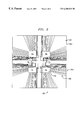
- FIG. 3 is a diagrammatic plan view of the optical signal processing apparatus including four 16 ⁇ 16 mirror array chips.
- FIG. 4 is an elevational side view of a hybrid electro-optic assembly.
- a mirror array chip 10 which includes a substrate 11 , a plurality of mirrors 12 positioned on the substrate 11 , and a plurality of electrical lead lines 14 extending from each mirror 12 to connection points 14 a beyond the periphery of the substrate 11 .
- the substrate 11 can be, for example, a silicon wafer.
- Such mirror array chips are known to those with skill in the art.
- the mirrors 12 are typically fabricated by micro-machining and are movable from one angular orientation to another in response to the application thereto of an electrostatic force. Electrical leads (at least two, and preferably four per mirror) carry the electrical charge to the mirror. By individually regulating the charges on the electrical lead lines 14 the position of the mirrors can be individually adjusted as desired.
- the mirrors 12 can be of any appropriate shape (e.g., circular, square, rectangular, and the like), and can be of any suitable size, but typically range in diameter from about 100 to 1,000 ⁇ m, preferably 200 to 800 ⁇ m, and more preferably 400 to 600 ⁇ m.
- the center to center spacing of the mirrors 12 can be any dimension greater than one mirror diameter, but typically ranges from 1.5 mirror diameters to about 3 mirror diameters, preferably from 1.75 mirror diameters to about 2.25 mirror diameters.
- the spacing between the edge of one mirror and the edge of its closest neighboring mirror can range from about 100 to 1,000 ⁇ m, preferably 200 to 800 ⁇ m, and more preferably 400 to 600 ⁇ m.
- the mirror array chip 10 can be used, for example, in optical cross connect applications in which light beams from a bundle of optical fibers are individually directed onto each mirror 12 .
- the mirrors 12 are individually adjustable to deflect the light beams to predetermined optical receivers, such as another bundle of optical fibers.
- Mirror array chip 10 shown in FIG. 1 is a 3 ⁇ 3 mirror array containing 9 mirrors, of which 8 mirrors are peripheral and 1 mirror is interior.
- the electrical lead lines of the interior mirror must extend through the space between two other mirrors.
- the number of mirrors in an array is increased, the number of interior mirrors dramatically increases.
- the lead lines to the 196 interior mirrors must be routed through the spaces between mirrors. Since the wires carry a relatively high electrostatic voltage (e.g., typically 100-150 volts) there must be adequate spacing between the lead lines 14 .
- the practical limiting size of the mirror array chip is 16 ⁇ 16, i.e., a 256 mirror array.
- the length of each side of a 256 mirror array chip of square shape with 500 ⁇ m diameter mirrors is about 2 cm.
- To increase the size of the array would require increased spacing between mirrors, which undesirably decreases the mirror density of the array.
- the invention described herein increases the capacity of the optical cross connect to accommodate fiber optic bundles with over 1,000 optical fibers yet still retaining a high mirror density.
- a support 100 which includes a base 101 , and a plurality of secondary leads 103 each corresponding to a respective lead line 14 and forming a continuous electrical connection.
- Base 101 can be silicon, high density multilayered thin film sheet, ceramic, or standard circuit boards.
- the support 100 has an edge length or a diameter of several inches.
- the secondary leads 103 extend from the connection points 14 a towards connection points 103 a the periphery 100 a of support 100 . Manufacturing techniques for fabricating a support and for affixing a mirror array chip thereto are known in the art.
- secondary leads 103 fan outward as they approach the periphery 100 a so that the spacing between the secondary leads 103 is greater near periphery 100 a than at the edges of the mirror array chips 10 .
- the greater spacing between the secondary lead lines near periphery 100 a facilitates the use of wirebonding and soldering as methods for electrically connecting the secondary leads 103 to other electrical components. Soldering, for example, requires a spacing of about 200 ⁇ m between lead lines, which cannot be readily achieved on the mirror array chip 10 itself.
- a significant feature of the present invention is that at least a portion of the secondary lead lines 103 traverse the spaces 10 a , 10 b , 10 c , and 10 d , onto which the respective mirror array chips 10 are positioned.
- the secondary lead lines 103 extend beneath the mirror array chips 10 and between the bottom surface of the respective mirror array chip and the top surface of the base 101 , thereby exploiting an additional area of space. Use of this additional area beneath the mirror array chips 10 enables at least two, and preferably four mirror array chips 10 to be positioned in close proximity, thereby forming a compound array of greater capacity.
- a compound, square multichip array 200 which includes 1024 mirror elements 210 in four separate 16 ⁇ 16 mirror array chips 211 , 212 , 213 , 214 and more than 4,000 wirebond pads and electrical connections (not shown), positioned on a base 220 .
- Length L is no more than about 4 cm.
- Multichip array 200 therefore has a 1,024 mirror capacity at a density of about 64 mirrors per square cm.
- a hybrid, multi-layered electro-optic structure 300 which includes a plurality of mirror array chips 301 defining a first layer 300 a positioned on a base 302 defining a second layer 300 b , the mirror array chips 301 being electrically connected thereto to form a compound, multichip array.
- a plurality of wirebonds 303 electrically connect the electrical leads of the base 302 to a wafer 304 defining a third layer 300 c supporting an integrated signal processing circuit.
- Optional vias 305 electrically connect the integrated circuit of wafer 304 to a printed circuit on board 307 defining a fourth layer 300 d.
- Discrete passive and/or active electronic components 306 may optionally be incorporated into the circuit on board 307 .
- Such components can include, for example, transistors, rectifiers, capacitors, inductors, batteries, and the like.
- Cable connectors 308 a and 308 b provide electrical power and/or electrical signals to the structure 300 from a source (not shown).
- the electrical circuits on wafer 304 and board 307 direct electrical signals to the individual mirrors and may included decoding functions.
- the layers of the structure 300 can be individually fabricated from single or double sided silicon wafers, flex tape, multi-layered ceramics, and multi-layered circuit boards.
- a bundle of optical fibers 309 a transmits light to the mirror array chips 301 , each optical fiber individually directing a beam of light to a respective one of the mirrors in the mirror array chips 301 .
- the mirrors are controlled by electronic signals to individually direct the light beams to a respective one of the optical fibers of bundle 309 b. Over 1,000 fibers can be in each bundle.
- the light beams can be used, for example, in visual displays, or as carriers of digital information in telecommunication networks.
Abstract
Description
Claims (18)
Priority Applications (4)
| Application Number | Priority Date | Filing Date | Title |
|---|---|---|---|
| US09/410,586 US6288821B1 (en) | 1999-10-01 | 1999-10-01 | Hybrid electro-optic device with combined mirror arrays |
| EP00308118A EP1093004A3 (en) | 1999-10-01 | 2000-09-18 | Hybrid electro-optic device with combined mirror arrays |
| CA002321021A CA2321021A1 (en) | 1999-10-01 | 2000-09-27 | Hybrid electro-optic device with combined mirror arrays |
| JP2000298177A JP2001147386A (en) | 1999-10-01 | 2000-09-29 | Optical signal processor |
Applications Claiming Priority (1)
| Application Number | Priority Date | Filing Date | Title |
|---|---|---|---|
| US09/410,586 US6288821B1 (en) | 1999-10-01 | 1999-10-01 | Hybrid electro-optic device with combined mirror arrays |
Publications (1)
| Publication Number | Publication Date |
|---|---|
| US6288821B1 true US6288821B1 (en) | 2001-09-11 |
Family
ID=23625372
Family Applications (1)
| Application Number | Title | Priority Date | Filing Date |
|---|---|---|---|
| US09/410,586 Expired - Lifetime US6288821B1 (en) | 1999-10-01 | 1999-10-01 | Hybrid electro-optic device with combined mirror arrays |
Country Status (4)
| Country | Link |
|---|---|
| US (1) | US6288821B1 (en) |
| EP (1) | EP1093004A3 (en) |
| JP (1) | JP2001147386A (en) |
| CA (1) | CA2321021A1 (en) |
Cited By (4)
| Publication number | Priority date | Publication date | Assignee | Title |
|---|---|---|---|---|
| US6522801B1 (en) * | 2000-10-10 | 2003-02-18 | Agere Systems Inc. | Micro-electro-optical mechanical device having an implanted dopant included therein and a method of manufacture therefor |
| US6668109B2 (en) * | 2000-09-07 | 2003-12-23 | Teraop Inc. | Method and system for ultra-fast switching of optical signals |
| US20070279731A1 (en) * | 2006-06-06 | 2007-12-06 | Girsh Blumberg | Light wave front construction |
| US8803861B2 (en) | 2012-02-23 | 2014-08-12 | Qualcomm Mems Technologies, Inc. | Electromechanical systems device |
Families Citing this family (2)
| Publication number | Priority date | Publication date | Assignee | Title |
|---|---|---|---|---|
| AU2002363793A1 (en) * | 2001-11-09 | 2003-05-26 | Movaz Networks, Inc. | Multi-chip module integrating mems mirror array with electronics |
| JP4550653B2 (en) * | 2005-04-15 | 2010-09-22 | 富士通株式会社 | Micro movable element and optical switching device |
Citations (24)
| Publication number | Priority date | Publication date | Assignee | Title |
|---|---|---|---|---|
| US4229732A (en) | 1978-12-11 | 1980-10-21 | International Business Machines Corporation | Micromechanical display logic and array |
| US4698602A (en) | 1985-10-09 | 1987-10-06 | The United States Of America As Represented By The Secretary Of The Air Force | Micromirror spatial light modulator |
| US5054870A (en) | 1989-04-03 | 1991-10-08 | Alcatel N.V. | Electro-optical multiple connection arrangement |
| US5199087A (en) | 1991-12-31 | 1993-03-30 | Texas Instruments Incorporated | Optoelectronic integrated circuit for transmitting optical and electrical signals and method of forming same |
| US5237434A (en) | 1991-11-05 | 1993-08-17 | Mcnc | Microelectronic module having optical and electrical interconnects |
| US5357122A (en) | 1991-09-05 | 1994-10-18 | Sony Corporation | Three-dimensional optical-electronic integrated circuit device with raised sections |
| US5416870A (en) | 1993-12-03 | 1995-05-16 | Motorola, Inc. | Optoelectronic interface device and method with reflective surface |
| US5572540A (en) | 1992-08-11 | 1996-11-05 | University Of New Mexico | Two-dimensional opto-electronic switching arrays |
| US5608826A (en) | 1994-06-09 | 1997-03-04 | Apa Optics, Inc. | Wavelength division multiplexed optical modulator and multiplexing method using same |
| US5611006A (en) | 1993-08-31 | 1997-03-11 | Fujitsu Limited | Hybrid type integrated optical device having double-layered substrate |
| US5623564A (en) | 1995-06-07 | 1997-04-22 | Lucent Technologies Inc. | Self-aligned mechanical optical switch |
| US5627923A (en) | 1993-09-16 | 1997-05-06 | Hitachi, Ltd. | Three-dimensional opto-electric integrated circuit using optical wiring |
| US5708741A (en) | 1995-12-28 | 1998-01-13 | Lucent Technologies Inc. | Method and apparatus for coupling optical fibers to an optical integrated circuit |
| US5719976A (en) | 1995-10-24 | 1998-02-17 | Lucent Technologies, Inc. | Optimized waveguide structure |
| US5761350A (en) | 1997-01-22 | 1998-06-02 | Koh; Seungug | Method and apparatus for providing a seamless electrical/optical multi-layer micro-opto-electro-mechanical system assembly |
| US5790731A (en) | 1995-04-13 | 1998-08-04 | Lucent Technologies Inc. | Optical fiber array/optical integrated circuit interconnection assembly and enclosures for protecting the interconnection assembly |
| US5799120A (en) | 1995-12-04 | 1998-08-25 | Nec Corporation | Waveguide type wavelength multiplexing/demultiplexing module |
| US5828800A (en) | 1997-06-23 | 1998-10-27 | Lucent Technologies Inc. | Self-aligned mechanical M×N optical switch |
| US5835256A (en) | 1995-06-19 | 1998-11-10 | Reflectivity, Inc. | Reflective spatial light modulator with encapsulated micro-mechanical elements |
| US5863809A (en) | 1997-03-28 | 1999-01-26 | Lucent Technologies Inc. | Manufacture of planar photonic integrated circuits |
| US5917645A (en) * | 1997-03-28 | 1999-06-29 | Daewoo Electronics Co., Ltd. | Thin film actuated mirror array in an optical projection system and method for manufacturing the same |
| US5923798A (en) | 1997-05-15 | 1999-07-13 | Lucent Technologies, Inc. | Micro machined optical switch |
| US6097859A (en) * | 1998-02-12 | 2000-08-01 | The Regents Of The University Of California | Multi-wavelength cross-connect optical switch |
| US6107979A (en) * | 1995-01-17 | 2000-08-22 | Texas Instruments Incorporated | Monolithic programmable format pixel array |
Family Cites Families (5)
| Publication number | Priority date | Publication date | Assignee | Title |
|---|---|---|---|---|
| FR2368054A1 (en) * | 1976-10-13 | 1978-05-12 | Comp Generale Electricite | METHOD FOR INCREASING THE ILLUMINATION PRODUCED BY A LASER BEAM |
| US5182632A (en) * | 1989-11-22 | 1993-01-26 | Tactical Fabs, Inc. | High density multichip package with interconnect structure and heatsink |
| US5796377A (en) * | 1990-04-03 | 1998-08-18 | Aura Systems, Inc. | Video display system having an electronic switch matrix for controlling an M×N array of piezoelectric members |
| US5671083A (en) * | 1995-02-02 | 1997-09-23 | Texas Instruments Incorporated | Spatial light modulator with buried passive charge storage cell array |
| US6011639A (en) * | 1997-11-06 | 2000-01-04 | Raytheon Company | One piece deformable mirror actuator assembly |
-
1999
- 1999-10-01 US US09/410,586 patent/US6288821B1/en not_active Expired - Lifetime
-
2000
- 2000-09-18 EP EP00308118A patent/EP1093004A3/en not_active Withdrawn
- 2000-09-27 CA CA002321021A patent/CA2321021A1/en not_active Abandoned
- 2000-09-29 JP JP2000298177A patent/JP2001147386A/en active Pending
Patent Citations (24)
| Publication number | Priority date | Publication date | Assignee | Title |
|---|---|---|---|---|
| US4229732A (en) | 1978-12-11 | 1980-10-21 | International Business Machines Corporation | Micromechanical display logic and array |
| US4698602A (en) | 1985-10-09 | 1987-10-06 | The United States Of America As Represented By The Secretary Of The Air Force | Micromirror spatial light modulator |
| US5054870A (en) | 1989-04-03 | 1991-10-08 | Alcatel N.V. | Electro-optical multiple connection arrangement |
| US5357122A (en) | 1991-09-05 | 1994-10-18 | Sony Corporation | Three-dimensional optical-electronic integrated circuit device with raised sections |
| US5237434A (en) | 1991-11-05 | 1993-08-17 | Mcnc | Microelectronic module having optical and electrical interconnects |
| US5199087A (en) | 1991-12-31 | 1993-03-30 | Texas Instruments Incorporated | Optoelectronic integrated circuit for transmitting optical and electrical signals and method of forming same |
| US5572540A (en) | 1992-08-11 | 1996-11-05 | University Of New Mexico | Two-dimensional opto-electronic switching arrays |
| US5611006A (en) | 1993-08-31 | 1997-03-11 | Fujitsu Limited | Hybrid type integrated optical device having double-layered substrate |
| US5627923A (en) | 1993-09-16 | 1997-05-06 | Hitachi, Ltd. | Three-dimensional opto-electric integrated circuit using optical wiring |
| US5416870A (en) | 1993-12-03 | 1995-05-16 | Motorola, Inc. | Optoelectronic interface device and method with reflective surface |
| US5608826A (en) | 1994-06-09 | 1997-03-04 | Apa Optics, Inc. | Wavelength division multiplexed optical modulator and multiplexing method using same |
| US6107979A (en) * | 1995-01-17 | 2000-08-22 | Texas Instruments Incorporated | Monolithic programmable format pixel array |
| US5790731A (en) | 1995-04-13 | 1998-08-04 | Lucent Technologies Inc. | Optical fiber array/optical integrated circuit interconnection assembly and enclosures for protecting the interconnection assembly |
| US5623564A (en) | 1995-06-07 | 1997-04-22 | Lucent Technologies Inc. | Self-aligned mechanical optical switch |
| US5835256A (en) | 1995-06-19 | 1998-11-10 | Reflectivity, Inc. | Reflective spatial light modulator with encapsulated micro-mechanical elements |
| US5719976A (en) | 1995-10-24 | 1998-02-17 | Lucent Technologies, Inc. | Optimized waveguide structure |
| US5799120A (en) | 1995-12-04 | 1998-08-25 | Nec Corporation | Waveguide type wavelength multiplexing/demultiplexing module |
| US5708741A (en) | 1995-12-28 | 1998-01-13 | Lucent Technologies Inc. | Method and apparatus for coupling optical fibers to an optical integrated circuit |
| US5761350A (en) | 1997-01-22 | 1998-06-02 | Koh; Seungug | Method and apparatus for providing a seamless electrical/optical multi-layer micro-opto-electro-mechanical system assembly |
| US5863809A (en) | 1997-03-28 | 1999-01-26 | Lucent Technologies Inc. | Manufacture of planar photonic integrated circuits |
| US5917645A (en) * | 1997-03-28 | 1999-06-29 | Daewoo Electronics Co., Ltd. | Thin film actuated mirror array in an optical projection system and method for manufacturing the same |
| US5923798A (en) | 1997-05-15 | 1999-07-13 | Lucent Technologies, Inc. | Micro machined optical switch |
| US5828800A (en) | 1997-06-23 | 1998-10-27 | Lucent Technologies Inc. | Self-aligned mechanical M×N optical switch |
| US6097859A (en) * | 1998-02-12 | 2000-08-01 | The Regents Of The University Of California | Multi-wavelength cross-connect optical switch |
Cited By (5)
| Publication number | Priority date | Publication date | Assignee | Title |
|---|---|---|---|---|
| US6668109B2 (en) * | 2000-09-07 | 2003-12-23 | Teraop Inc. | Method and system for ultra-fast switching of optical signals |
| US6522801B1 (en) * | 2000-10-10 | 2003-02-18 | Agere Systems Inc. | Micro-electro-optical mechanical device having an implanted dopant included therein and a method of manufacture therefor |
| US20070279731A1 (en) * | 2006-06-06 | 2007-12-06 | Girsh Blumberg | Light wave front construction |
| US7619808B2 (en) | 2006-06-06 | 2009-11-17 | Alcatel-Lucent Usa Inc. | Light wave front construction |
| US8803861B2 (en) | 2012-02-23 | 2014-08-12 | Qualcomm Mems Technologies, Inc. | Electromechanical systems device |
Also Published As
| Publication number | Publication date |
|---|---|
| EP1093004A3 (en) | 2003-04-02 |
| EP1093004A2 (en) | 2001-04-18 |
| CA2321021A1 (en) | 2001-04-01 |
| JP2001147386A (en) | 2001-05-29 |
Similar Documents
| Publication | Publication Date | Title |
|---|---|---|
| US6396711B1 (en) | Interconnecting micromechanical devices | |
| US4580873A (en) | Optical matrix switch | |
| US6599031B2 (en) | Optical/electrical interconnects and package for high speed signaling | |
| EP0567209B1 (en) | Liquid crystal panel module and tape carrier package | |
| JPH0393258A (en) | Three-dimensional integrated circuit construction using discrete chip | |
| US5047830A (en) | Field emitter array integrated circuit chip interconnection | |
| CA2129762C (en) | Opto-electronic hybrid integration platform, optical sub-module, opto-electronic hybrid integration circuit, and process for fabricating platform | |
| US4858072A (en) | Interconnection system for integrated circuit chips | |
| CN101578703A (en) | Wafer-level fabrication of lidded chips with electrodeposited dielectric coating | |
| US6288821B1 (en) | Hybrid electro-optic device with combined mirror arrays | |
| US5612575A (en) | Method of connecting the output pads on an integrated circuit chip, and multichip module thus obtained | |
| US7208771B2 (en) | Separating of optical integrated modules and structures formed thereby | |
| US6347167B1 (en) | Fiber optic cross connect with uniform redirection length and folding of light beams | |
| JPH06295977A (en) | Wiring for electric power and signal in electronic package | |
| US20030026553A1 (en) | Optical chip packaging via through hole | |
| US6525864B1 (en) | Integrated mirror array and circuit device | |
| AU4517193A (en) | Component module | |
| US6374007B1 (en) | Double hermetic package for fiber optic cross connect | |
| US6617243B1 (en) | Routing for multilayer ceramic substrates to reduce excessive via depth | |
| US5451812A (en) | Leadframe for semiconductor devices | |
| EP1425945B1 (en) | Pin-free socket compatible with optical-electrical interconnects | |
| US7046936B2 (en) | Light receiving element carrier and optical receiver | |
| US6687132B2 (en) | Conductive member grid array interface for mirror array drive apparatus | |
| US6396973B1 (en) | Fiber optic cross connect with transparent substrate | |
| US6447174B1 (en) | Active optical interconnect |
Legal Events
| Date | Code | Title | Description |
|---|---|---|---|
| AS | Assignment |
Owner name: LUCENT TECHNOLOGIES INC., NEW JERSEY Free format text: ASSIGNMENT OF ASSIGNORS INTEREST;ASSIGNORS:AKSYUK, VLADIMIR ANATOLYEVICH;BISHOP, DAVID JOHN;BOLLE, CRISTIAN A.;AND OTHERS;REEL/FRAME:010433/0307;SIGNING DATES FROM 19991112 TO 19991130 |
|
| STCF | Information on status: patent grant |
Free format text: PATENTED CASE |
|
| FPAY | Fee payment |
Year of fee payment: 4 |
|
| FEPP | Fee payment procedure |
Free format text: PAYOR NUMBER ASSIGNED (ORIGINAL EVENT CODE: ASPN); ENTITY STATUS OF PATENT OWNER: LARGE ENTITY |
|
| FPAY | Fee payment |
Year of fee payment: 8 |
|
| FPAY | Fee payment |
Year of fee payment: 12 |
|
| AS | Assignment |
Owner name: CREDIT SUISSE AG, NEW YORK Free format text: SECURITY INTEREST;ASSIGNOR:ALCATEL-LUCENT USA INC.;REEL/FRAME:030510/0627 Effective date: 20130130 |
|
| AS | Assignment |
Owner name: DEUTSCHE BANK AG NEW YORK BRANCH, AS COLLATERAL AG Free format text: PATENT SECURITY AGREEMENT;ASSIGNORS:LSI CORPORATION;AGERE SYSTEMS LLC;REEL/FRAME:032856/0031 Effective date: 20140506 |
|
| AS | Assignment |
Owner name: ALCATEL-LUCENT USA INC., NEW JERSEY Free format text: RELEASE BY SECURED PARTY;ASSIGNOR:CREDIT SUISSE AG;REEL/FRAME:033949/0531 Effective date: 20140819 |
|
| AS | Assignment |
Owner name: AVAGO TECHNOLOGIES GENERAL IP (SINGAPORE) PTE. LTD Free format text: ASSIGNMENT OF ASSIGNORS INTEREST;ASSIGNOR:AGERE SYSTEMS LLC;REEL/FRAME:035365/0634 Effective date: 20140804 |
|
| AS | Assignment |
Owner name: AGERE SYSTEMS LLC, PENNSYLVANIA Free format text: TERMINATION AND RELEASE OF SECURITY INTEREST IN PATENT RIGHTS (RELEASES RF 032856-0031);ASSIGNOR:DEUTSCHE BANK AG NEW YORK BRANCH, AS COLLATERAL AGENT;REEL/FRAME:037684/0039 Effective date: 20160201 Owner name: LSI CORPORATION, CALIFORNIA Free format text: TERMINATION AND RELEASE OF SECURITY INTEREST IN PATENT RIGHTS (RELEASES RF 032856-0031);ASSIGNOR:DEUTSCHE BANK AG NEW YORK BRANCH, AS COLLATERAL AGENT;REEL/FRAME:037684/0039 Effective date: 20160201 |
|
| AS | Assignment |
Owner name: BANK OF AMERICA, N.A., AS COLLATERAL AGENT, NORTH CAROLINA Free format text: PATENT SECURITY AGREEMENT;ASSIGNOR:AVAGO TECHNOLOGIES GENERAL IP (SINGAPORE) PTE. LTD.;REEL/FRAME:037808/0001 Effective date: 20160201 Owner name: BANK OF AMERICA, N.A., AS COLLATERAL AGENT, NORTH Free format text: PATENT SECURITY AGREEMENT;ASSIGNOR:AVAGO TECHNOLOGIES GENERAL IP (SINGAPORE) PTE. LTD.;REEL/FRAME:037808/0001 Effective date: 20160201 |
|
| AS | Assignment |
Owner name: AVAGO TECHNOLOGIES GENERAL IP (SINGAPORE) PTE. LTD., SINGAPORE Free format text: TERMINATION AND RELEASE OF SECURITY INTEREST IN PATENTS;ASSIGNOR:BANK OF AMERICA, N.A., AS COLLATERAL AGENT;REEL/FRAME:041710/0001 Effective date: 20170119 Owner name: AVAGO TECHNOLOGIES GENERAL IP (SINGAPORE) PTE. LTD Free format text: TERMINATION AND RELEASE OF SECURITY INTEREST IN PATENTS;ASSIGNOR:BANK OF AMERICA, N.A., AS COLLATERAL AGENT;REEL/FRAME:041710/0001 Effective date: 20170119 |
|
| AS | Assignment |
Owner name: AVAGO TECHNOLOGIES INTERNATIONAL SALES PTE. LIMITE Free format text: ASSIGNMENT OF ASSIGNORS INTEREST;ASSIGNOR:AVAGO TECHNOLOGIES GENERAL IP (SINGAPORE) PTE. LTD.;REEL/FRAME:047022/0620 Effective date: 20180509 |
|
| AS | Assignment |
Owner name: AVAGO TECHNOLOGIES INTERNATIONAL SALES PTE. LIMITE Free format text: CORRECTIVE ASSIGNMENT TO CORRECT THE NATURE OF CONVEYANCE AND EFFECTIVE DATE PREVIOUSLY RECORDED ON REEL 047022 FRAME 0620. ASSIGNOR(S) HEREBY CONFIRMS THE MERGER;ASSIGNOR:AVAGO TECHNOLOGIES GENERAL IP (SINGAPORE) PTE. LTD.;REEL/FRAME:047185/0643 Effective date: 20180509 |
|
| AS | Assignment |
Owner name: AVAGO TECHNOLOGIES INTERNATIONAL SALES PTE. LIMITE Free format text: CORRECTIVE ASSIGNMENT TO CORRECT THE EFFECTIVE DATE PREVIOUSLY RECORDED ON REEL 047185 FRAME 0643. ASSIGNOR(S) HEREBY CONFIRMS THE MERGER;ASSIGNOR:AVAGO TECHNOLOGIES GENERAL IP (SINGAPORE) PTE. LTD.;REEL/FRAME:047476/0845 Effective date: 20180905 |
|
| AS | Assignment |
Owner name: AVAGO TECHNOLOGIES INTERNATIONAL SALES PTE. LIMITE Free format text: CORRECTIVE ASSIGNMENT TO CORRECT THE EFFECTIVE DATE OF MERGER PREVIOUSLY RECORDED AT REEL: 047185 FRAME: 0643. ASSIGNOR(S) HEREBY CONFIRMS THE CORRECTIVE MERGER;ASSIGNOR:AVAGO TECHNOLOGIES GENERAL IP (SINGAPORE) PTE. LTD.;REEL/FRAME:047959/0296 Effective date: 20180905 |