US6282111B1 - Inverter control using current mode slope modulation - Google Patents
Inverter control using current mode slope modulation Download PDFInfo
- Publication number
- US6282111B1 US6282111B1 US09/335,977 US33597799A US6282111B1 US 6282111 B1 US6282111 B1 US 6282111B1 US 33597799 A US33597799 A US 33597799A US 6282111 B1 US6282111 B1 US 6282111B1
- Authority
- US
- United States
- Prior art keywords
- signal
- output
- sine wave
- amplitude
- inverter
- Prior art date
- Legal status (The legal status is an assumption and is not a legal conclusion. Google has not performed a legal analysis and makes no representation as to the accuracy of the status listed.)
- Expired - Fee Related
Links
- 230000006835 compression Effects 0.000 claims abstract description 13
- 238000007906 compression Methods 0.000 claims abstract description 13
- 239000003990 capacitor Substances 0.000 claims description 16
- 230000002238 attenuated effect Effects 0.000 claims description 4
- 238000006243 chemical reaction Methods 0.000 abstract description 6
- 230000008859 change Effects 0.000 description 5
- 238000010586 diagram Methods 0.000 description 5
- 238000000034 method Methods 0.000 description 5
- 230000010355 oscillation Effects 0.000 description 5
- 230000033228 biological regulation Effects 0.000 description 4
- 230000008901 benefit Effects 0.000 description 3
- 239000000470 constituent Substances 0.000 description 2
- 230000000694 effects Effects 0.000 description 2
- 230000005611 electricity Effects 0.000 description 2
- 230000007935 neutral effect Effects 0.000 description 2
- 230000010363 phase shift Effects 0.000 description 2
- 230000009467 reduction Effects 0.000 description 2
- 239000004065 semiconductor Substances 0.000 description 2
- XUIMIQQOPSSXEZ-UHFFFAOYSA-N Silicon Chemical compound [Si] XUIMIQQOPSSXEZ-UHFFFAOYSA-N 0.000 description 1
- 230000009471 action Effects 0.000 description 1
- 230000002146 bilateral effect Effects 0.000 description 1
- 230000000052 comparative effect Effects 0.000 description 1
- 238000012937 correction Methods 0.000 description 1
- 230000001351 cycling effect Effects 0.000 description 1
- 230000007423 decrease Effects 0.000 description 1
- 230000001934 delay Effects 0.000 description 1
- 238000013461 design Methods 0.000 description 1
- 238000007599 discharging Methods 0.000 description 1
- 230000005669 field effect Effects 0.000 description 1
- 238000001914 filtration Methods 0.000 description 1
- 238000005259 measurement Methods 0.000 description 1
- 229910044991 metal oxide Inorganic materials 0.000 description 1
- 150000004706 metal oxides Chemical class 0.000 description 1
- 230000004048 modification Effects 0.000 description 1
- 238000012986 modification Methods 0.000 description 1
- 238000013021 overheating Methods 0.000 description 1
- 239000013641 positive control Substances 0.000 description 1
- 229910052710 silicon Inorganic materials 0.000 description 1
- 239000010703 silicon Substances 0.000 description 1
- 230000001360 synchronised effect Effects 0.000 description 1
- 230000007704 transition Effects 0.000 description 1
- 238000004804 winding Methods 0.000 description 1
Images


Classifications
-
- H—ELECTRICITY
- H02—GENERATION; CONVERSION OR DISTRIBUTION OF ELECTRIC POWER
- H02M—APPARATUS FOR CONVERSION BETWEEN AC AND AC, BETWEEN AC AND DC, OR BETWEEN DC AND DC, AND FOR USE WITH MAINS OR SIMILAR POWER SUPPLY SYSTEMS; CONVERSION OF DC OR AC INPUT POWER INTO SURGE OUTPUT POWER; CONTROL OR REGULATION THEREOF
- H02M7/00—Conversion of AC power input into DC power output; Conversion of DC power input into AC power output
- H02M7/42—Conversion of DC power input into AC power output without possibility of reversal
- H02M7/44—Conversion of DC power input into AC power output without possibility of reversal by static converters
- H02M7/48—Conversion of DC power input into AC power output without possibility of reversal by static converters using discharge tubes with control electrode or semiconductor devices with control electrode
- H02M7/53—Conversion of DC power input into AC power output without possibility of reversal by static converters using discharge tubes with control electrode or semiconductor devices with control electrode using devices of a triode or transistor type requiring continuous application of a control signal
- H02M7/537—Conversion of DC power input into AC power output without possibility of reversal by static converters using discharge tubes with control electrode or semiconductor devices with control electrode using devices of a triode or transistor type requiring continuous application of a control signal using semiconductor devices only, e.g. single switched pulse inverters
- H02M7/5387—Conversion of DC power input into AC power output without possibility of reversal by static converters using discharge tubes with control electrode or semiconductor devices with control electrode using devices of a triode or transistor type requiring continuous application of a control signal using semiconductor devices only, e.g. single switched pulse inverters in a bridge configuration
- H02M7/53871—Conversion of DC power input into AC power output without possibility of reversal by static converters using discharge tubes with control electrode or semiconductor devices with control electrode using devices of a triode or transistor type requiring continuous application of a control signal using semiconductor devices only, e.g. single switched pulse inverters in a bridge configuration with automatic control of output voltage or current
Definitions
- the present invention relates to power inverters and DC to DC converters and, more specifically, to both improved power inverters and DC to DC converters operating in current mode utilizing a novel slope modulation regulation scheme.
- Inverters change one type of electrical current into another.
- DC direct current
- AC alternating current
- DC direct current
- AC alternating current
- Direct current is current which flows in the same direction at all points in time. If one were to measure the voltage of a DC circuit at different instants in time, the measurement would remain constant. As mentioned, the advantage of DC is that it is easy to store.
- Alternating current is current which periodically reverses its direction of movement over various periods of time. If one were to measure the voltage of an AC circuit at different instants in time, the voltage would fluctuate, being in a cycle of continuous reversal. In the U.S. this cycling occurs 60 times per second, i.e., 60 Hz.
- the advantages of AC are that it is very easy to step voltages up or down (through transformers) and thus easier to distribute over long distances with smaller wire than would be possible with DC. This is because as electricity is carried, energy is thermally dissipated due to the resistance of the wire. However, the relative loss decreases as the voltage increases.
- DC must be converted into AC to power appliances and other wall powered devices. This is the role inverters play. Many methods of DC to AC conversion are well known in the art. However, they all present serious shortcomings that the present invention addresses in a novel fashion.
- High frequency switched DC to AC inverters generally use a voltage controlled pulse width modulation scheme such as the system 100 exemplified in FIG. 1 (FIG. 1) wherein DC current enters at terminals 108 and AC current leaves at terminals 109 .
- This system has a full bridge configuration of switching transistors and commutating diodes 106 .
- Said bridge could, for example, comprise transistors of type Bipolar, IGBT (insulated gate bipolar transistor), MOSFET (metal-oxide semiconductor field effect transistor), or gate controlled SCR (silicon controlled rectifier). Said bridge is then connected to an LC (inductor and capacitor) output filter 107 .
- the semiconductors are enabled by conventional drive circuitry 105 .
- the circuit operates by pulse width modulating a constant frequency drive to the switching transistors in such a way that the average output from them, when smoothed by the LC filter 107 , is the required low frequency sine wave.
- a sawtooth generator 102 provides a constant frequency constant amplitude sawtooth ramp signal derived from a conventional relaxation oscillator operating at the required high switching frequency.
- a low voltage reference sine wave is generated by 101 by conventional means and has a peak to peak amplitude slightly less than that of the sawtooth ramp. In the case of a DC to DC converter the sine wave reference is replaced by a DC voltage reference.
- the sine wave or DC voltage reference and sawtooth reference are then compared by a conventional analog comparator 104 which acts here as a pulse width modulator to generate a pulse width modulated logic level signal which if passed through a low pass filter will accurately reproduce the sine wave or DC reference.
- the modulated signal is then buffered and isolated by the transistor drive circuits 105 for connection to the bridge power switching transistors and commutating diodes 106 .
- An LC filter 107 removes high frequency components to leave a low frequency sinusoidal or DC voltage output.
- FIG. 2 shows a modification of the voltage controlled pulse width modulated system 200 to allow current mode control wherein DC current enters at terminals 108 and AC or DC current leaves at terminals 109 .
- a current sense point 201 is inserted between the switching power transistors 106 and the LC output filter 107 to provide a reference voltage proportional to the instantaneous current.
- the inverter or DC to DC converter output voltage at terminals 109 is compared to a reference sine wave by an error amplifier 202 .
- the intention is to make the current flowing through the power switches 106 proportional to this error voltage and as a consequence the power stage becomes a high impedance current source; the output inductor impedance is absorbed into the high impedance source and thus the maximum phase shift through said filter 107 is now only 90 degrees compared to 180 degrees for a voltage control system.
- This signal is now compared with a high frequency sawtooth reference by comparator/pulse width modulator 104 and the high frequency digital output is connected to the transistor drive circuits 105 as in the above disclosed voltage controlled pulse width modulated inverter 100 .
- hysteretic current control Another method known in the art for DC to AC inverters is hysteretic current control.
- High performance high frequency switching inverters and DC to DC converters require gain around the control loop at frequencies many multiples of the baseband sine wave. This is particularly true in the case of inverters driving non-linear loads such as diode rectifiers with capacitor filters for which a high loop gain at frequencies greater than ten or twenty times the baseband frequency is essential if the waveform distortion is to be minimized.
- Hysteretic current control achieves such performance without becoming prone to subharmonic oscillations. Unfortunately it does not work well at switching frequencies above 50 kHz where circuit delays and power component switching times become so long that circuit currents change significantly between the time that a specific current level is measured and the actual change of state in the power circuits.
- FIG. 3A shows the operation of a two state bridge power stage 400 in detail.
- Q 1 , Q 2 , Q 3 , and Q 4 are the switching elements and L and C form the output low pass filter 107 .
- the drive circuits are connected so that at one time Q 1 and Q 4 are switched on with Q 2 and Q 3 switched off. In the other switching phase, Q 1 and Q 4 are switched off with Q 2 and Q 3 switched on.
- FIG. 3B the voltage at D mirrors that at C and the switching losses are identical for both bridge halves, Q 1 , Q 2 and Q 3 , Q 4 .
- the first embodiment of the present invention retains several functions of previously disclosed current controlled inverter or DC to DC converter with pulse width modulation 200 (see FIG. 2.)
- Sine wave generator 101 , error amplifier 202 , difference amplifier 203 , and drive circuits 105 all operate as previously disclosed.
- the sawtooth generator 102 and comparator/pulse width modulator 104 are replaced with a new circuit that pulse width modulates by varying the rise and fall times of a sawtooth generator.
- Such a pulse width modulation system is not constrained in time and by allowing the frequency to vary there is no susceptibility to subharmonic oscillation. It has advantages over hysteretic current mode operation in that noise components in the current sense and current command signals, which cause enormous problems in hysteretic control, are to a great degree eliminated. This is because the control signals are currents that charge the timing capacitor.
- this novel modulation scheme allows the present invention to be used as a DC-DC converter as well as an inverter. To effect DC-DC conversion the sine wave reference signal is simply replaced with a DC reference signal.
- FIG. 4 shows typical inverter AC output voltages with DC input levels below that necessary for an undistorted output; the tops and bottoms of the sine waves are clipped off.
- FIG. 5 shows comparative waveforms for a system using sine wave reference compression in which the output is always sinusoidal with the maximum value that can be achieved for any particular input.
- Another object of this invention is to provide an improved DC-DC power converter utilizing current mode control using slope modulation.
- FIG. 1 (FIG. 1 ), above disclosed, is a combination block and schematic diagram of a voltage controlled inverter with pulse width modulation
- FIG. 2 (FIG. 2 ), above disclosed, is a combination block and schematic diagram of a current controlled inverter with pulse width modulation
- FIG. 3A depicts a two state modulation circuit
- FIG. 3B depicts exemplary waveforms of said two state modulation circuit
- FIG. 4 depicts waveforms exemplary of prior art inverters with insufficient and sufficient DC input voltage
- FIG. 5 depicts waveforms exemplary of an inverter in accordance with the present invention using sine wave reference compression with varying degrees of DC input voltage;
- FIG. 6A is a combination block and schematic diagram of a current controlled inverter with slope modulation in accordance with the present invention
- FIG. 6B depicts exemplary waveforms constituent to the present invention
- FIG. 7A depicts a schematic of a three state modulation circuit
- FIG. 7B depicts waveforms exemplary of said three state modulation circuit
- FIG. 8A depicts a schematic of the low frequency drive used in said three state modulation circuit
- FIG. 8B depicts waveforms exemplary of said low frequency drive circuit
- FIG. 9 depicts a combination schematic and block diagram of an isolated voltage sense circuit in accordance with the present invention.
- FIG. 10 depicts a combination schematic and block diagram of an alternate embodiment of the isolated voltage sense capable of working at high voltages in accordance with the present invention.
- FIG. 11 depicts a schematic of the sine wave compression circuit in accordance with the present invention.
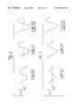
- FIG. 6A schematically depicts a first embodiment of a power inverter 300 in accordance with the present disclosure.
- the heart of system 300 is a multivibrator 303 with comparator U 1 and components R 1 , R 2 , R 3 , and C 1 . Values are chosen for operations at the nominal switching frequency, and the logic level output at point ‘B’ is a square wave with a 50-50 duty cycle.
- This oscillator is modulated by speeding up either the rise time or fall time depending on whether the inverter output is to go positive or negative. Speeding up the rise time will result in a reduction in the time that ‘B’ is positive compared with the negative duration. This pulse width modulation results in the inverter output being taken negative.
- the charging rates are controlled by two current sources, one to pull positive 301 and one to pull negative 302 .
- the currents are made proportional to the positive or negative output from the current difference amplifier 203 .
- These two current sources 301 and 302 are gated with U 1 output so that the positive current source is only operational when C 1 is charging and the negative current source is operational only when C 2 is discharging.
- logic level inverter U 2 functions to enable negative current source 302 when the positive current source 301 is disabled, and conversely, disables negative current source 302 when the positive current source 301 is enabled.
- Analog inverter U 3 reverses the polarity of the output signal from difference amplifier 203 and in turn is connected to the negative current source 302 .
- Current sources 301 and 302 operate such that a negative input results in a low output current and a positive input results in a high output current.
- the positive current from it will rapidly charge capacitor C 1 .
- the analog control signal is inverted by U 3 to be a negative signal input to the negative current source 302 resulting in a low negative current to discharge capacitor C 1 .
- Capacitor C 1 will therefore discharge slowly. Under these conditions signal B from multivibrator 303 is positive for a long time as capacitor C 1 discharges slowly and negative for a short time as capacitor C 1 charges rapidly.
- FIG. 6B depicts waveforms characteristic of the present invention.
- Waveform 610 shows the unmodulated signal at point ‘A’ when the control voltages to the current sources 301 and 302 are zero.
- Waveform 611 depicts the signal at point ‘A’ when the control voltage from the difference amplifier 203 is a low frequency sine wave.
- Towards the left hand side a positive control voltage leads to a high current from positive current source 301 and capacitor C 1 charges rapidly.
- the corresponding low current from negative current source 302 results in a slow discharge.
- the resulting output at point ‘B’ 612 has a short positive “on” time and a long negative “off” time.
- waveform 612 Toward the center of waveform 612 , equal currents from 301 and 302 lead to equal “on” and “off” times at point ‘B’.
- the right side of waveform 612 occurs when there is a low positive current from 301 and a high negative current from 302 leading to a long “on” time at point ‘B’ and a corresponding short “off” time.
- Waveform 612 when low pass filtered, is a low frequency sine wave as shown by the dotted line 613 .
- FIG. 7A shows a three state switching DC to AC inverter power stage while FIG. 7B shows characteristic waveforms.
- the power stage is similar to the two state system with the exception that the filter inductor L constituent of output filter 501 now needs only half the inductance of that for a two state system to achieve the same output ripple.
- the drive circuits are changed so that now the side of the bridge allocated to low speed switching Q 5 , Q 6 is enabled by signal LS and its compliment LS′ and that associated with high speed switching, Q 7 , Q 8 is enabled by signal HS and its compliment HS′.
- the waveform at point ‘F’ 506 is a square wave at the low output frequency whereas the waveform at ‘G’ 507 represents alternate positive and negative pulse width modulated half cycles.
- the waveform generated 508 when waveform 506 and waveform 507 are added together and low pass filtered by filter 501 is a low frequency sine wave 509 .
- the waveform at ‘F’ 506 is not a pure square wave but includes a few high frequency switching pulses at each positive to negative and negative to positive transition in order to cover the control circuit's rapid change of pulse width modulation requirement from mostly turned on to mostly turned off, and vice versa, in a very short time.
- FIG. 8A depicts a schematic of the low speed drive 600 which provides signals LS and LS′, while FIG. 8B depicts characteristic waveforms.
- the sine wave reference signal 605 (see FIG. 6A, sine wave generator 101 ) is connected to one side 603 of a voltage comparator 601 and a ramp signal 606 attenuated by attenuator 604 is connected from the slope modulator (see FIG. 6 A, point ‘A’) to the other input 602 .
- the resulting output is a square wave 607 with high frequency bursts as the signal changes state.
- the bursts are automatically pulse width modulated and are synchronized with the high speed switching. Varying the attenuator varies the width of the high frequency burst and the duration of the burst is determined by the slew rate of the control circuits at low frequency zero crossings.
- the sine wave compression circuit has two major components; one to measure the DC voltage, and the other to vary the sine wave voltage.
- a simple inverter configuration having a half bridge configuration with both positive and negative DC inputs with commons connected to the output neutral does not have DC levels that are referenced to the inverter control.
- the DC input voltage reference can be a resistive divider.
- Such an inverter unfortunately incurs the highest switching losses and high voltage stress on the switching components and so is seldom used.
- Other configurations such as full bridge two state and three state systems have DC input voltages that do not have a simple relationship to the AC output neutral; the common point for the sine wave reference. It is possible to derive a DC signal proportional to the DC input, but it is simpler to design an isolated measuring system.
- FIG. 9 depicts the isolated voltage sense 900 .
- the active element Q 9 is driven at high frequencies, typically 100 kHz by a drive circuit 1100 having a 50-50 duty cycle.
- Transformer T 1 has a square wave across its primary winding 1 - 2 .
- T 1 secondary When diode D 1 is connected and the DC inverter supply voltage is zero T 1 secondary is effectively shorted out when Q 9 is tuned on. Transformer T 1 is wound for low loss and low leakage inductance so the short across the secondary 3 - 4 is transferred back to the primary 1 - 2 . The short 1 - 2 in series with turned on transistor Q 9 pulls point ‘I’ down to the control supply negative voltage.
- T 1 secondary voltage rise is controlled by the clamping action D 1 .
- the voltage at point ‘I’ rises by an amount determined by the transformer ratio 3 - 4 to 1 - 2 .
- the voltage at ‘I’ is proportional to the inverter DC input.
- FIG. 10 shows a variant 1000 of the circuit 900 in which the voltage to be sensed is first attenuated by R 6 and R 7 and then an emitter follower Q 11 is used to catch the secondary clamp diode D 2 .
- the voltage at ‘I’ is now the ratio R 3 to R 2 +R 3 multiplied by T 2 primary to secondary ratio.
- the drive circuit 1100 serves the identical purpose as in FIG. 9 .
- Components R 5 , C 4 and Q 10 serve identical purpose to R 4 , C 2 and Q 9 in FIG. 9 but may have different component values.
- the sine wave compression circuit pulse width modulates the sine wave reference and then low pass filters the result to produce a reduced voltage but undistorted output.
- This circuit 1100 is depicted schematically in FIG. 11 .
- Comparator U 4 together with R 8 , R 9 , R 10 and C 5 act as a 100 kHz multivibrator 1101 .
- the digital output serves to drive the switching transistor, Q 9 or Q 1 O on FIGS. 9 and 10, respectively.
- the sawtooth signal is connected to the negative input of a second comparator U 5 .
- the U 5 positive input ‘K’ is connected to the reference signal, either point ‘I’ on FIG. 9 or point ‘J’ on FIG. 10, depending on the voltage level used.
- Circuit values are adjusted so that when the inverter DC input voltage is as high or higher than that required for a full sine wave output the voltage at ‘K’ is greater than the positive excursion of the ramp signal at ‘L’.
- U 5 output is positive and a bilateral switch U 6 connects the sine wave reference at ‘N’ to the low pass filter 1102 comprising R 11 and C 6 then out to the inverter at ‘P’.
- the reference ‘K’ is less than the peak positive value of the ramp signal at ‘L’, and the output of U 2 at ‘M’ is a pulse width modulated signal.
- pulse width modulates the reference at ‘N’ by periodically disabling switch U 3 to produce the signal at ‘O’.
- Low pass filtering by 1102 smooths out the chopped sine wave to provide a reduced amplitude reference. Careful component selection allows the sine wave reference output to be made proportional to the inverter DC input voltage when it is below the critical level.
Landscapes
- Engineering & Computer Science (AREA)
- Power Engineering (AREA)
- Inverter Devices (AREA)
Abstract
Description
Claims (14)
Priority Applications (1)
| Application Number | Priority Date | Filing Date | Title |
|---|---|---|---|
| US09/335,977 US6282111B1 (en) | 1999-06-18 | 1999-06-18 | Inverter control using current mode slope modulation |
Applications Claiming Priority (1)
| Application Number | Priority Date | Filing Date | Title |
|---|---|---|---|
| US09/335,977 US6282111B1 (en) | 1999-06-18 | 1999-06-18 | Inverter control using current mode slope modulation |
Publications (1)
| Publication Number | Publication Date |
|---|---|
| US6282111B1 true US6282111B1 (en) | 2001-08-28 |
Family
ID=23314046
Family Applications (1)
| Application Number | Title | Priority Date | Filing Date |
|---|---|---|---|
| US09/335,977 Expired - Fee Related US6282111B1 (en) | 1999-06-18 | 1999-06-18 | Inverter control using current mode slope modulation |
Country Status (1)
| Country | Link |
|---|---|
| US (1) | US6282111B1 (en) |
Cited By (24)
| Publication number | Priority date | Publication date | Assignee | Title |
|---|---|---|---|---|
| US20030090912A1 (en) * | 2001-10-31 | 2003-05-15 | Luis Zubieta | Transformerless two-phase inverter |
| US20030169109A1 (en) * | 2002-03-11 | 2003-09-11 | Uis Abler Electronics Co., Ltd. | Active harmonic suppression equipment and control method therefor |
| WO2003081759A1 (en) * | 2002-03-27 | 2003-10-02 | Commergy Technologies Limited | 'a power converter' |
| US20030193821A1 (en) * | 2002-04-10 | 2003-10-16 | Michael Krieger | Inverter for producing a true sine wave |
| US6664774B2 (en) * | 2002-03-27 | 2003-12-16 | Semtech Corporation | Offset peak current mode control circuit for multiple-phase power converter |
| US20040204173A1 (en) * | 2002-05-31 | 2004-10-14 | Catena Networks, Inc. | Apparatus and method of controlling low frequency load currents drawn from a DC source in a telecommunications system |
| US6912144B1 (en) * | 2004-08-19 | 2005-06-28 | International Rectifier Corporation | Method and apparatus for adjusting current amongst phases of a multi-phase converter |
| US20050270000A1 (en) * | 2004-03-31 | 2005-12-08 | Liuchen Chang | Single-stage buck-boost inverter |
| US7265530B1 (en) | 2003-11-07 | 2007-09-04 | National Semiconductor Corporation | Adaptive slope compensation for switching regulators |
| US20070296348A1 (en) * | 2006-06-15 | 2007-12-27 | Walker James T | Current driven bipolar high voltage driver for capacitive loads |
| US20080298104A1 (en) * | 2007-06-04 | 2008-12-04 | Sustainable Energy Technologies | Prediction scheme for step wave power converter and inductive inverter topology |
| US20090166451A1 (en) * | 2007-12-27 | 2009-07-02 | Lindsay Corporation | Wind-Powered Irrigation Machine |
| US20090201703A1 (en) * | 2008-02-07 | 2009-08-13 | Damir Klikic | Systems and Methods for Uninterruptible Power Supply Control |
| US7808125B1 (en) | 2006-07-31 | 2010-10-05 | Sustainable Energy Technologies | Scheme for operation of step wave power converter |
| US20100289481A1 (en) * | 2009-05-13 | 2010-11-18 | Silicon Motion, Inc. | Apparatus and method for dc voltage measurement |
| US8422249B2 (en) | 2011-08-25 | 2013-04-16 | Direct Grid Technologies, LLC | Apparatus for a microinverter particularly suited for use in solar power installations |
| US20150207433A1 (en) * | 2014-01-22 | 2015-07-23 | Lite-On Electronics (Guangzhou) Limited | Single-phase three-wire power control system and power control method therefor |
| WO2015138744A1 (en) * | 2014-03-13 | 2015-09-17 | Qatar Foundation For Education, Science And Community Development | Modulation and control methods for quasi-z-source cascade multilevel inverters |
| WO2016050685A1 (en) * | 2014-10-02 | 2016-04-07 | TRUMPF Hüttinger GmbH + Co. KG | Method for operating an mf power generator, and an mf power generator |
| US20160105128A1 (en) * | 2014-10-10 | 2016-04-14 | The Regents Of The University Of California | Robust single-phase DC/AC inverter for highly varying DC voltages |
| US20170324249A1 (en) * | 2016-05-09 | 2017-11-09 | Sungrow Power Supply Co., Ltd. | Ac-dc photovoltaic device |
| CN107565676A (en) * | 2016-07-01 | 2018-01-09 | 阳光电源股份有限公司 | A kind of photovoltaic apparatus and photovoltaic system |
| US10447346B2 (en) * | 2016-10-12 | 2019-10-15 | Samsung Electro-Mechanics Co., Ltd. | Inverter and wireless power transmitter using the same |
| US11362599B2 (en) * | 2020-02-15 | 2022-06-14 | National Tsing Hua University | Controlling method for single-phase bidirectional inverter and device thereof |
-
1999
- 1999-06-18 US US09/335,977 patent/US6282111B1/en not_active Expired - Fee Related
Cited By (48)
| Publication number | Priority date | Publication date | Assignee | Title |
|---|---|---|---|---|
| US6643156B2 (en) * | 2001-10-31 | 2003-11-04 | Global Thermoelectric Inc. | Transformerless two-phase inverter |
| US20030090912A1 (en) * | 2001-10-31 | 2003-05-15 | Luis Zubieta | Transformerless two-phase inverter |
| US20030169109A1 (en) * | 2002-03-11 | 2003-09-11 | Uis Abler Electronics Co., Ltd. | Active harmonic suppression equipment and control method therefor |
| US6717465B2 (en) * | 2002-03-11 | 2004-04-06 | Uis Abler Electronics Co., Ltd. | Active harmonic suppression equipment and control method therefor |
| US20050231254A1 (en) * | 2002-03-27 | 2005-10-20 | Commergy Technologies Limited | Power converter |
| WO2003081759A1 (en) * | 2002-03-27 | 2003-10-02 | Commergy Technologies Limited | 'a power converter' |
| US6664774B2 (en) * | 2002-03-27 | 2003-12-16 | Semtech Corporation | Offset peak current mode control circuit for multiple-phase power converter |
| US7277305B2 (en) | 2002-03-27 | 2007-10-02 | Commergy Technologies Limited | Power converter |
| US20030193821A1 (en) * | 2002-04-10 | 2003-10-16 | Michael Krieger | Inverter for producing a true sine wave |
| US20040204173A1 (en) * | 2002-05-31 | 2004-10-14 | Catena Networks, Inc. | Apparatus and method of controlling low frequency load currents drawn from a DC source in a telecommunications system |
| US6980783B2 (en) * | 2002-05-31 | 2005-12-27 | Ciena Corporation | Apparatus and method of controlling low frequency load currents drawn from a DC source in a telecommunications system |
| US7479778B1 (en) | 2003-11-07 | 2009-01-20 | National Semiconductor Corporation | Adaptive slope compensation for switching regulators |
| US7589517B1 (en) | 2003-11-07 | 2009-09-15 | National Semiconductor Corporation | Adaptive slope compensation for switching regulators |
| US7265530B1 (en) | 2003-11-07 | 2007-09-04 | National Semiconductor Corporation | Adaptive slope compensation for switching regulators |
| US7307412B1 (en) | 2003-11-07 | 2007-12-11 | National Semiconductor Corporation | Inductive measurement system and method |
| US20050270000A1 (en) * | 2004-03-31 | 2005-12-08 | Liuchen Chang | Single-stage buck-boost inverter |
| US6912144B1 (en) * | 2004-08-19 | 2005-06-28 | International Rectifier Corporation | Method and apparatus for adjusting current amongst phases of a multi-phase converter |
| WO2006023522A1 (en) * | 2004-08-19 | 2006-03-02 | International Rectifier Corporation | Method and apparatus for adjusting current amongst phases of a multi-phase converter |
| US20070296348A1 (en) * | 2006-06-15 | 2007-12-27 | Walker James T | Current driven bipolar high voltage driver for capacitive loads |
| US8154898B2 (en) * | 2006-06-15 | 2012-04-10 | Supertex, Inc. | Current driven bipolar high voltage driver for capacitive loads |
| US7808125B1 (en) | 2006-07-31 | 2010-10-05 | Sustainable Energy Technologies | Scheme for operation of step wave power converter |
| US8026639B1 (en) | 2006-07-31 | 2011-09-27 | Sustainable Energy Technologies | Scheme for operation of step wave power converter |
| US20080298104A1 (en) * | 2007-06-04 | 2008-12-04 | Sustainable Energy Technologies | Prediction scheme for step wave power converter and inductive inverter topology |
| WO2009044293A3 (en) * | 2007-06-04 | 2009-12-30 | Sustainable Energy Technologies | Prediction scheme for step wave power converter and inductive inverter topology |
| CN101790827B (en) * | 2007-06-04 | 2013-06-12 | 可持续能源技术公司 | Prediction scheme for step wave power converter and inductive inverter topology |
| US8031495B2 (en) | 2007-06-04 | 2011-10-04 | Sustainable Energy Technologies | Prediction scheme for step wave power converter and inductive inverter topology |
| US20090166451A1 (en) * | 2007-12-27 | 2009-07-02 | Lindsay Corporation | Wind-Powered Irrigation Machine |
| US20090201703A1 (en) * | 2008-02-07 | 2009-08-13 | Damir Klikic | Systems and Methods for Uninterruptible Power Supply Control |
| US8116105B2 (en) * | 2008-02-07 | 2012-02-14 | American Power Conversion Corporation | Systems and methods for uninterruptible power supply control |
| US20100289481A1 (en) * | 2009-05-13 | 2010-11-18 | Silicon Motion, Inc. | Apparatus and method for dc voltage measurement |
| US8324884B2 (en) * | 2009-05-13 | 2012-12-04 | Silicon Motion, Inc. | Apparatus and method for DC voltage measurement |
| US8422249B2 (en) | 2011-08-25 | 2013-04-16 | Direct Grid Technologies, LLC | Apparatus for a microinverter particularly suited for use in solar power installations |
| US9413270B2 (en) * | 2014-01-22 | 2016-08-09 | Lite-On Electronics (Guangzhou) Limited | Single-phase three-wire power control system and power control method therefor |
| US20150207433A1 (en) * | 2014-01-22 | 2015-07-23 | Lite-On Electronics (Guangzhou) Limited | Single-phase three-wire power control system and power control method therefor |
| WO2015138744A1 (en) * | 2014-03-13 | 2015-09-17 | Qatar Foundation For Education, Science And Community Development | Modulation and control methods for quasi-z-source cascade multilevel inverters |
| US10027126B2 (en) | 2014-03-13 | 2018-07-17 | Qatar Foundation For Education, Science And Community Development | Modulation and control methods for quasi-Z-source cascade multilevel inverters |
| WO2016050685A1 (en) * | 2014-10-02 | 2016-04-07 | TRUMPF Hüttinger GmbH + Co. KG | Method for operating an mf power generator, and an mf power generator |
| US9876442B2 (en) * | 2014-10-10 | 2018-01-23 | The Regents Of The University Of California | Robust single-phase DC/AC inverter for highly varying DC voltages |
| US20160105128A1 (en) * | 2014-10-10 | 2016-04-14 | The Regents Of The University Of California | Robust single-phase DC/AC inverter for highly varying DC voltages |
| US20170324249A1 (en) * | 2016-05-09 | 2017-11-09 | Sungrow Power Supply Co., Ltd. | Ac-dc photovoltaic device |
| EP3244523A1 (en) * | 2016-05-09 | 2017-11-15 | Sungrow Power Supply Co., Ltd. | Alternating-current direct-current photovoltaic device |
| CN107359855A (en) * | 2016-05-09 | 2017-11-17 | 阳光电源股份有限公司 | A kind of photovoltaic apparatus of AC/DC |
| US10389132B2 (en) * | 2016-05-09 | 2019-08-20 | Sungrow Power Supply Co., Ltd. | AC-DC photovoltaic device |
| CN107359855B (en) * | 2016-05-09 | 2020-01-21 | 阳光电源股份有限公司 | Dual-purpose photovoltaic equipment of alternating current-direct current |
| CN107565676A (en) * | 2016-07-01 | 2018-01-09 | 阳光电源股份有限公司 | A kind of photovoltaic apparatus and photovoltaic system |
| CN107565676B (en) * | 2016-07-01 | 2020-01-21 | 阳光电源股份有限公司 | Photovoltaic equipment and photovoltaic system |
| US10447346B2 (en) * | 2016-10-12 | 2019-10-15 | Samsung Electro-Mechanics Co., Ltd. | Inverter and wireless power transmitter using the same |
| US11362599B2 (en) * | 2020-02-15 | 2022-06-14 | National Tsing Hua University | Controlling method for single-phase bidirectional inverter and device thereof |
Similar Documents
| Publication | Publication Date | Title |
|---|---|---|
| US6282111B1 (en) | Inverter control using current mode slope modulation | |
| JP2583258B2 (en) | Method and apparatus for electrostatic power conversion | |
| US4833584A (en) | Quasi-resonant current mode static power conversion method and apparatus | |
| US5038267A (en) | Soft-switching power converter for operation in discrete pulse modulation and pulse width modulation modes | |
| US6310787B2 (en) | Multiway power converter | |
| JP3427385B2 (en) | High frequency AC / AC converter with power factor correction | |
| US5761055A (en) | Driving pulse output limiting circuit | |
| US4903181A (en) | Power converter having parallel power switching systems coupled by an impedance inversion network | |
| US8503204B2 (en) | Power converter circuit | |
| US20100328967A1 (en) | Resonant power converter | |
| JPH0197169A (en) | High-frequency resonance type power converter | |
| US6477062B1 (en) | Power supply unit including an inverter | |
| EP0553179A1 (en) | Dc/ac converter. | |
| JPH0851790A (en) | Control circuit for inductive load | |
| GB2265732A (en) | Power converter with waveform control | |
| US4688165A (en) | Current fed inverter bridge with conduction overlap and load tuning | |
| US20230074022A1 (en) | Power converter topologies with power factor correction circuits controlled using adjustable deadtime | |
| He et al. | Novel high-efficiency frequency-variable buck–boost AC–AC converter with safe-commutation and continuous current | |
| Lai et al. | A novel resonant snubber based soft-switching inverter | |
| US5181160A (en) | Driving circuit for inverter microwave oven | |
| CN114448286A (en) | Single-stage isolation bidirectional AC-DC converter topological structure and control method thereof | |
| US5237492A (en) | AC to DC converter system with ripple feedback circuit | |
| US20230071003A1 (en) | Power factor correction circuits controlled using adjustable deadtime | |
| Ruan et al. | A novel zero-voltage and zero-current-switching PWM three-level converter | |
| Park et al. | Study on the new control scheme of class-E inverter for IH-jar application with clamped voltage characteristics using pulse frequency modulation |
Legal Events
| Date | Code | Title | Description |
|---|---|---|---|
| AS | Assignment |
Owner name: AVIONIC INSTRUMENTS, INC., NEW JERSEY Free format text: ASSIGNMENT OF ASSIGNORS INTEREST;ASSIGNOR:ILLINGWORTH, LEWIS;REEL/FRAME:010684/0785 Effective date: 19991118 |
|
| AS | Assignment |
Owner name: AVIONIC INSTRUMENTS, INC., NEW JERSEY Free format text: ASSIGNMENT OF ASSIGNORS INTEREST;ASSIGNOR:ILLINGWORTH, LEWIS;REEL/FRAME:011727/0880 Effective date: 20010405 |
|
| AS | Assignment |
Owner name: AVIONIC INSTRUMENTS, INC., NEW JERSEY Free format text: CORRECTIVE ASSIGNMENT TO CORRECT THE ASSIGNEES ADDRESS PREVIOUSLY RECORDED AT REEL 011727 FRAME 0880;ASSIGNOR:ILLINGWORTH, LEWIS;REEL/FRAME:012068/0630 Effective date: 20010405 |
|
| REMI | Maintenance fee reminder mailed | ||
| LAPS | Lapse for failure to pay maintenance fees | ||
| STCH | Information on status: patent discontinuation |
Free format text: PATENT EXPIRED DUE TO NONPAYMENT OF MAINTENANCE FEES UNDER 37 CFR 1.362 |
|
| AS | Assignment |
Owner name: CREDIT SUISSE, AS COLLATERAL AGENT, NEW YORK Free format text: SECURITY AGREEMENT;ASSIGNOR:AVIONIC INSTRUMENTS INC.;REEL/FRAME:016621/0266 Effective date: 20050926 |
|
| FP | Lapsed due to failure to pay maintenance fee |
Effective date: 20050828 |
|
| AS | Assignment |
Owner name: CREDIT SUISSE, CAYMAN ISLANDS BRANCH, NEW YORK Free format text: SECURITY AGREEMENT;ASSIGNOR:AVIONIC INSTRUMENTS INC.;REEL/FRAME:017833/0284 Effective date: 20060623 |
|
| AS | Assignment |
Owner name: THE BANK OF NEW YORK MELLON TRUST COMPANY, N.A.,, Free format text: SECURITY INTEREST;ASSIGNORS:TRANSDIGM, INC.;ADAMS RITE AEROSPACE, INC.;AEROCONTROLEX GROUP, INC.;AND OTHERS;REEL/FRAME:048365/0499 Effective date: 20190214 |
|
| AS | Assignment |
Owner name: THE BANK OF NEW YORK MELLON TRUST COMPANY, N.A., AS TRUSTEE AND NOTES COLLATERAL AGENT, ILLINOIS Free format text: PATENT SECURITY AGREEMENT;ASSIGNORS:AIRBORNE SYSTEMS NORTH AMERICA OF NJ INC.;ACME AEROSPACE, INC.;ADAMS RITE AEROSPACE, INC.;AND OTHERS;REEL/FRAME:052352/0704 Effective date: 20200408 |
|
| AS | Assignment |
Owner name: APICAL INDUSTRIES, INC., OHIO Free format text: RELEASE BY SECURED PARTY;ASSIGNOR:THE BANK OF NEW YORK MELLON TRUST COMPANY, N.A., AS TRUSTEE;REEL/FRAME:063363/0753 Effective date: 20230410 Owner name: SIMPLEX MANUFACTURING CO., OHIO Free format text: RELEASE BY SECURED PARTY;ASSIGNOR:THE BANK OF NEW YORK MELLON TRUST COMPANY, N.A., AS TRUSTEE;REEL/FRAME:063363/0753 Effective date: 20230410 Owner name: CHELTON, INC. (N/K/A CHELTON AVIONICS, INC.), ARIZONA Free format text: RELEASE BY SECURED PARTY;ASSIGNOR:THE BANK OF NEW YORK MELLON TRUST COMPANY, N.A., AS TRUSTEE;REEL/FRAME:063363/0753 Effective date: 20230410 Owner name: PALOMAR PRODUCTS, INC., CALIFORNIA Free format text: RELEASE BY SECURED PARTY;ASSIGNOR:THE BANK OF NEW YORK MELLON TRUST COMPANY, N.A., AS TRUSTEE;REEL/FRAME:063363/0753 Effective date: 20230410 Owner name: KORRY ELECTRONICS CO., WASHINGTON Free format text: RELEASE BY SECURED PARTY;ASSIGNOR:THE BANK OF NEW YORK MELLON TRUST COMPANY, N.A., AS TRUSTEE;REEL/FRAME:063363/0753 Effective date: 20230410 Owner name: MASON ELECTRIC CO., CALIFORNIA Free format text: RELEASE BY SECURED PARTY;ASSIGNOR:THE BANK OF NEW YORK MELLON TRUST COMPANY, N.A., AS TRUSTEE;REEL/FRAME:063363/0753 Effective date: 20230410 Owner name: TA AEROSPACE CO., CALIFORNIA Free format text: RELEASE BY SECURED PARTY;ASSIGNOR:THE BANK OF NEW YORK MELLON TRUST COMPANY, N.A., AS TRUSTEE;REEL/FRAME:063363/0753 Effective date: 20230410 Owner name: NMC GROUP INC., CALIFORNIA Free format text: RELEASE BY SECURED PARTY;ASSIGNOR:THE BANK OF NEW YORK MELLON TRUST COMPANY, N.A., AS TRUSTEE;REEL/FRAME:063363/0753 Effective date: 20230410 Owner name: LEACH INTERNATIONAL CORPORATION, CALIFORNIA Free format text: RELEASE BY SECURED PARTY;ASSIGNOR:THE BANK OF NEW YORK MELLON TRUST COMPANY, N.A., AS TRUSTEE;REEL/FRAME:063363/0753 Effective date: 20230410 Owner name: ARMTEC DEFENSE PRODUCTS COMPANY, CALIFORNIA Free format text: RELEASE BY SECURED PARTY;ASSIGNOR:THE BANK OF NEW YORK MELLON TRUST COMPANY, N.A., AS TRUSTEE;REEL/FRAME:063363/0753 Effective date: 20230410 Owner name: ARMTEC COUNTERMEASURES CO., NORTH CAROLINA Free format text: RELEASE BY SECURED PARTY;ASSIGNOR:THE BANK OF NEW YORK MELLON TRUST COMPANY, N.A., AS TRUSTEE;REEL/FRAME:063363/0753 Effective date: 20230410 Owner name: YOUNG & FRANKLIN INC., NEW YORK Free format text: RELEASE BY SECURED PARTY;ASSIGNOR:THE BANK OF NEW YORK MELLON TRUST COMPANY, N.A., AS TRUSTEE;REEL/FRAME:063363/0753 Effective date: 20230410 Owner name: WHIPPANY ACTUATION SYSTEMS, LLC, NEW JERSEY Free format text: RELEASE BY SECURED PARTY;ASSIGNOR:THE BANK OF NEW YORK MELLON TRUST COMPANY, N.A., AS TRUSTEE;REEL/FRAME:063363/0753 Effective date: 20230410 Owner name: WESTERN SKY INDUSTRIES, LLC, KENTUCKY Free format text: RELEASE BY SECURED PARTY;ASSIGNOR:THE BANK OF NEW YORK MELLON TRUST COMPANY, N.A., AS TRUSTEE;REEL/FRAME:063363/0753 Effective date: 20230410 Owner name: TRANSCOIL LLC, PENNSYLVANIA Free format text: RELEASE BY SECURED PARTY;ASSIGNOR:THE BANK OF NEW YORK MELLON TRUST COMPANY, N.A., AS TRUSTEE;REEL/FRAME:063363/0753 Effective date: 20230410 Owner name: TELAIR INTERNATIONAL LLC, NEW YORK Free format text: RELEASE BY SECURED PARTY;ASSIGNOR:THE BANK OF NEW YORK MELLON TRUST COMPANY, N.A., AS TRUSTEE;REEL/FRAME:063363/0753 Effective date: 20230410 Owner name: TEAC AEROSPACE TECHNOLOGIES, INC., FLORIDA Free format text: RELEASE BY SECURED PARTY;ASSIGNOR:THE BANK OF NEW YORK MELLON TRUST COMPANY, N.A., AS TRUSTEE;REEL/FRAME:063363/0753 Effective date: 20230410 Owner name: TACTAIR FLUID CONTROLS INC., NEW YORK Free format text: RELEASE BY SECURED PARTY;ASSIGNOR:THE BANK OF NEW YORK MELLON TRUST COMPANY, N.A., AS TRUSTEE;REEL/FRAME:063363/0753 Effective date: 20230410 Owner name: SHIELD RESTRAINT SYSTEMS, INC., INDIANA Free format text: RELEASE BY SECURED PARTY;ASSIGNOR:THE BANK OF NEW YORK MELLON TRUST COMPANY, N.A., AS TRUSTEE;REEL/FRAME:063363/0753 Effective date: 20230410 Owner name: SEMCO INSTRUMENTS, INC., CONNECTICUT Free format text: RELEASE BY SECURED PARTY;ASSIGNOR:THE BANK OF NEW YORK MELLON TRUST COMPANY, N.A., AS TRUSTEE;REEL/FRAME:063363/0753 Effective date: 20230410 Owner name: SCHNELLER LLC, OHIO Free format text: RELEASE BY SECURED PARTY;ASSIGNOR:THE BANK OF NEW YORK MELLON TRUST COMPANY, N.A., AS TRUSTEE;REEL/FRAME:063363/0753 Effective date: 20230410 Owner name: PNEUDRAULICS, INC., CALIFORNIA Free format text: RELEASE BY SECURED PARTY;ASSIGNOR:THE BANK OF NEW YORK MELLON TRUST COMPANY, N.A., AS TRUSTEE;REEL/FRAME:063363/0753 Effective date: 20230410 Owner name: PEXCO AEROSPACE, INC., WASHINGTON Free format text: RELEASE BY SECURED PARTY;ASSIGNOR:THE BANK OF NEW YORK MELLON TRUST COMPANY, N.A., AS TRUSTEE;REEL/FRAME:063363/0753 Effective date: 20230410 Owner name: MARATHONNORCO AEROSPACE, INC., TEXAS Free format text: RELEASE BY SECURED PARTY;ASSIGNOR:THE BANK OF NEW YORK MELLON TRUST COMPANY, N.A., AS TRUSTEE;REEL/FRAME:063363/0753 Effective date: 20230410 Owner name: HARTWELL CORPORATION, CALIFORNIA Free format text: RELEASE BY SECURED PARTY;ASSIGNOR:THE BANK OF NEW YORK MELLON TRUST COMPANY, N.A., AS TRUSTEE;REEL/FRAME:063363/0753 Effective date: 20230410 Owner name: HARCO LLC, CONNECTICUT Free format text: RELEASE BY SECURED PARTY;ASSIGNOR:THE BANK OF NEW YORK MELLON TRUST COMPANY, N.A., AS TRUSTEE;REEL/FRAME:063363/0753 Effective date: 20230410 Owner name: HARCO LABORATORIES, INC., CONNECTICUT Free format text: RELEASE BY SECURED PARTY;ASSIGNOR:THE BANK OF NEW YORK MELLON TRUST COMPANY, N.A., AS TRUSTEE;REEL/FRAME:063363/0753 Effective date: 20230410 Owner name: ELECTROMECH TECHNOLOGIES LLC, KANSAS Free format text: RELEASE BY SECURED PARTY;ASSIGNOR:THE BANK OF NEW YORK MELLON TRUST COMPANY, N.A., AS TRUSTEE;REEL/FRAME:063363/0753 Effective date: 20230410 Owner name: DUKES AEROSPACE, INC., OHIO Free format text: RELEASE BY SECURED PARTY;ASSIGNOR:THE BANK OF NEW YORK MELLON TRUST COMPANY, N.A., AS TRUSTEE;REEL/FRAME:063363/0753 Effective date: 20230410 Owner name: DATA DEVICE CORPORATION, NEW YORK Free format text: RELEASE BY SECURED PARTY;ASSIGNOR:THE BANK OF NEW YORK MELLON TRUST COMPANY, N.A., AS TRUSTEE;REEL/FRAME:063363/0753 Effective date: 20230410 Owner name: CHAMPION AEROSPACE LLC, SOUTH CAROLINA Free format text: RELEASE BY SECURED PARTY;ASSIGNOR:THE BANK OF NEW YORK MELLON TRUST COMPANY, N.A., AS TRUSTEE;REEL/FRAME:063363/0753 Effective date: 20230410 Owner name: CEF INDUSTRIES, INC., ILLINOIS Free format text: RELEASE BY SECURED PARTY;ASSIGNOR:THE BANK OF NEW YORK MELLON TRUST COMPANY, N.A., AS TRUSTEE;REEL/FRAME:063363/0753 Effective date: 20230410 Owner name: BRUCE AEROSPACE, INC., NEVADA Free format text: RELEASE BY SECURED PARTY;ASSIGNOR:THE BANK OF NEW YORK MELLON TRUST COMPANY, N.A., AS TRUSTEE;REEL/FRAME:063363/0753 Effective date: 20230410 Owner name: BREEZE EASTERN CORPORATION, NEW JERSEY Free format text: RELEASE BY SECURED PARTY;ASSIGNOR:THE BANK OF NEW YORK MELLON TRUST COMPANY, N.A., AS TRUSTEE;REEL/FRAME:063363/0753 Effective date: 20230410 Owner name: BEAM'S INDUSTRIES, OKLAHOMA Free format text: RELEASE BY SECURED PARTY;ASSIGNOR:THE BANK OF NEW YORK MELLON TRUST COMPANY, N.A., AS TRUSTEE;REEL/FRAME:063363/0753 Effective date: 20230410 Owner name: AVTECH TYEE, INC., WASHINGTON Free format text: RELEASE BY SECURED PARTY;ASSIGNOR:THE BANK OF NEW YORK MELLON TRUST COMPANY, N.A., AS TRUSTEE;REEL/FRAME:063363/0753 Effective date: 20230410 Owner name: AVIONICS SPECIALTIES, INC., OHIO Free format text: RELEASE BY SECURED PARTY;ASSIGNOR:THE BANK OF NEW YORK MELLON TRUST COMPANY, N.A., AS TRUSTEE;REEL/FRAME:063363/0753 Effective date: 20230410 Owner name: AVIONIC INSTRUMENTS LLC, NEW JERSEY Free format text: RELEASE BY SECURED PARTY;ASSIGNOR:THE BANK OF NEW YORK MELLON TRUST COMPANY, N.A., AS TRUSTEE;REEL/FRAME:063363/0753 Effective date: 20230410 Owner name: ARKWIN INDUSTRIES, INC., NEW YORK Free format text: RELEASE BY SECURED PARTY;ASSIGNOR:THE BANK OF NEW YORK MELLON TRUST COMPANY, N.A., AS TRUSTEE;REEL/FRAME:063363/0753 Effective date: 20230410 Owner name: AMSAFE, INC., ARIZONA Free format text: RELEASE BY SECURED PARTY;ASSIGNOR:THE BANK OF NEW YORK MELLON TRUST COMPANY, N.A., AS TRUSTEE;REEL/FRAME:063363/0753 Effective date: 20230410 Owner name: AMSAFE COMMERCIAL PRODUCTS INC., INDIANA Free format text: RELEASE BY SECURED PARTY;ASSIGNOR:THE BANK OF NEW YORK MELLON TRUST COMPANY, N.A., AS TRUSTEE;REEL/FRAME:063363/0753 Effective date: 20230410 Owner name: AIRBORNE SYSTEMS NORTH AMERICA OF NJ INC., NEW JERSEY Free format text: RELEASE BY SECURED PARTY;ASSIGNOR:THE BANK OF NEW YORK MELLON TRUST COMPANY, N.A., AS TRUSTEE;REEL/FRAME:063363/0753 Effective date: 20230410 Owner name: AIRBORNE HOLDINGS, INC., OHIO Free format text: RELEASE BY SECURED PARTY;ASSIGNOR:THE BANK OF NEW YORK MELLON TRUST COMPANY, N.A., AS TRUSTEE;REEL/FRAME:063363/0753 Effective date: 20230410 Owner name: AEROSONIC CORPORATION, FLORIDA Free format text: RELEASE BY SECURED PARTY;ASSIGNOR:THE BANK OF NEW YORK MELLON TRUST COMPANY, N.A., AS TRUSTEE;REEL/FRAME:063363/0753 Effective date: 20230410 Owner name: AEROCONTROLEX GROUP, INC., OHIO Free format text: RELEASE BY SECURED PARTY;ASSIGNOR:THE BANK OF NEW YORK MELLON TRUST COMPANY, N.A., AS TRUSTEE;REEL/FRAME:063363/0753 Effective date: 20230410 Owner name: ADAMS RITE AEROSPACE, INC., CALIFORNIA Free format text: RELEASE BY SECURED PARTY;ASSIGNOR:THE BANK OF NEW YORK MELLON TRUST COMPANY, N.A., AS TRUSTEE;REEL/FRAME:063363/0753 Effective date: 20230410 Owner name: ACME AEROSPACE, INC., ARIZONA Free format text: RELEASE BY SECURED PARTY;ASSIGNOR:THE BANK OF NEW YORK MELLON TRUST COMPANY, N.A., AS TRUSTEE;REEL/FRAME:063363/0753 Effective date: 20230410 Owner name: TRANSDIGM GROUP INCORPORATED, OHIO Free format text: RELEASE BY SECURED PARTY;ASSIGNOR:THE BANK OF NEW YORK MELLON TRUST COMPANY, N.A., AS TRUSTEE;REEL/FRAME:063363/0753 Effective date: 20230410 Owner name: TRANSDIGM, INC., OHIO Free format text: RELEASE BY SECURED PARTY;ASSIGNOR:THE BANK OF NEW YORK MELLON TRUST COMPANY, N.A., AS TRUSTEE;REEL/FRAME:063363/0753 Effective date: 20230410 |
|
| AS | Assignment |
Owner name: CEF INDUSTRIES, INC., ILLINOIS Free format text: RELEASE OF PATENT SECURITY AGREEMENT RECORDED FEBRUARY 19, 2019 AT REEL/FRAME 048365/0499;ASSIGNOR:THE BANK OF NEW YORK MELLON TRUST COMPANY, N.A., AS TRUSTEE;REEL/FRAME:067640/0147 Effective date: 20240514 Owner name: SCHNELLER, INC., OHIO Free format text: RELEASE OF PATENT SECURITY AGREEMENT RECORDED FEBRUARY 19, 2019 AT REEL/FRAME 048365/0499;ASSIGNOR:THE BANK OF NEW YORK MELLON TRUST COMPANY, N.A., AS TRUSTEE;REEL/FRAME:067640/0147 Effective date: 20240514 Owner name: ACME AEROSPACE, INC., ARIZONA Free format text: RELEASE OF PATENT SECURITY AGREEMENT RECORDED FEBRUARY 19, 2019 AT REEL/FRAME 048365/0499;ASSIGNOR:THE BANK OF NEW YORK MELLON TRUST COMPANY, N.A., AS TRUSTEE;REEL/FRAME:067640/0147 Effective date: 20240514 Owner name: ADAMS RITE AEROSPACE, INC., CALIFORNIA Free format text: RELEASE OF PATENT SECURITY AGREEMENT RECORDED FEBRUARY 19, 2019 AT REEL/FRAME 048365/0499;ASSIGNOR:THE BANK OF NEW YORK MELLON TRUST COMPANY, N.A., AS TRUSTEE;REEL/FRAME:067640/0147 Effective date: 20240514 Owner name: CALSPAN SYSTEMS, LLC, VIRGINIA Free format text: RELEASE OF PATENT SECURITY AGREEMENT RECORDED FEBRUARY 19, 2019 AT REEL/FRAME 048365/0499;ASSIGNOR:THE BANK OF NEW YORK MELLON TRUST COMPANY, N.A., AS TRUSTEE;REEL/FRAME:067640/0147 Effective date: 20240514 Owner name: CALSPAN AERO SYSTEMS ENGINEERING, INC., MINNESOTA Free format text: RELEASE OF PATENT SECURITY AGREEMENT RECORDED FEBRUARY 19, 2019 AT REEL/FRAME 048365/0499;ASSIGNOR:THE BANK OF NEW YORK MELLON TRUST COMPANY, N.A., AS TRUSTEE;REEL/FRAME:067640/0147 Effective date: 20240514 Owner name: TELAIR US LLC, NORTH CAROLINA Free format text: RELEASE OF PATENT SECURITY AGREEMENT RECORDED FEBRUARY 19, 2019 AT REEL/FRAME 048365/0499;ASSIGNOR:THE BANK OF NEW YORK MELLON TRUST COMPANY, N.A., AS TRUSTEE;REEL/FRAME:067640/0147 Effective date: 20240514 Owner name: PEXCO AEROSPACE, INC., WASHINGTON Free format text: RELEASE OF PATENT SECURITY AGREEMENT RECORDED FEBRUARY 19, 2019 AT REEL/FRAME 048365/0499;ASSIGNOR:THE BANK OF NEW YORK MELLON TRUST COMPANY, N.A., AS TRUSTEE;REEL/FRAME:067640/0147 Effective date: 20240514 Owner name: HARCO, LLC (N/K/A HARCOSEMCO LLC), CONNECTICUT Free format text: RELEASE OF PATENT SECURITY AGREEMENT RECORDED FEBRUARY 19, 2019 AT REEL/FRAME 048365/0499;ASSIGNOR:THE BANK OF NEW YORK MELLON TRUST COMPANY, N.A., AS TRUSTEE;REEL/FRAME:067640/0147 Effective date: 20240514 Owner name: HARCOSEMCO LLC, CONNECTICUT Free format text: RELEASE OF PATENT SECURITY AGREEMENT RECORDED FEBRUARY 19, 2019 AT REEL/FRAME 048365/0499;ASSIGNOR:THE BANK OF NEW YORK MELLON TRUST COMPANY, N.A., AS TRUSTEE;REEL/FRAME:067640/0147 Effective date: 20240514 Owner name: AIRBORNE SYSTEMS NA, INC., OHIO Free format text: RELEASE OF PATENT SECURITY AGREEMENT RECORDED FEBRUARY 19, 2019 AT REEL/FRAME 048365/0499;ASSIGNOR:THE BANK OF NEW YORK MELLON TRUST COMPANY, N.A., AS TRUSTEE;REEL/FRAME:067640/0147 Effective date: 20240514 Owner name: AERO-INSTRUMENTS CO., LLC, OHIO Free format text: RELEASE OF PATENT SECURITY AGREEMENT RECORDED FEBRUARY 19, 2019 AT REEL/FRAME 048365/0499;ASSIGNOR:THE BANK OF NEW YORK MELLON TRUST COMPANY, N.A., AS TRUSTEE;REEL/FRAME:067640/0147 Effective date: 20240514 Owner name: APICAL INDUSTRIES, INC., OHIO Free format text: RELEASE OF PATENT SECURITY AGREEMENT RECORDED FEBRUARY 19, 2019 AT REEL/FRAME 048365/0499;ASSIGNOR:THE BANK OF NEW YORK MELLON TRUST COMPANY, N.A., AS TRUSTEE;REEL/FRAME:067640/0147 Effective date: 20240514 Owner name: SIMPLEX MANUFACTURING CO., OHIO Free format text: RELEASE OF PATENT SECURITY AGREEMENT RECORDED FEBRUARY 19, 2019 AT REEL/FRAME 048365/0499;ASSIGNOR:THE BANK OF NEW YORK MELLON TRUST COMPANY, N.A., AS TRUSTEE;REEL/FRAME:067640/0147 Effective date: 20240514 Owner name: CHELTON, INC. (N/K/A CHELTON AVIONICS, INC.), ARIZONA Free format text: RELEASE OF PATENT SECURITY AGREEMENT RECORDED FEBRUARY 19, 2019 AT REEL/FRAME 048365/0499;ASSIGNOR:THE BANK OF NEW YORK MELLON TRUST COMPANY, N.A., AS TRUSTEE;REEL/FRAME:067640/0147 Effective date: 20240514 Owner name: MEMTRON TECHNOLOGIES CO., MICHIGAN Free format text: RELEASE OF PATENT SECURITY AGREEMENT RECORDED FEBRUARY 19, 2019 AT REEL/FRAME 048365/0499;ASSIGNOR:THE BANK OF NEW YORK MELLON TRUST COMPANY, N.A., AS TRUSTEE;REEL/FRAME:067640/0147 Effective date: 20240514 Owner name: ROLLS-ROYCE PLC, UNITED KINGDOM Free format text: RELEASE OF PATENT SECURITY AGREEMENT RECORDED FEBRUARY 19, 2019 AT REEL/FRAME 048365/0499;ASSIGNOR:THE BANK OF NEW YORK MELLON TRUST COMPANY, N.A., AS TRUSTEE;REEL/FRAME:067640/0147 Effective date: 20240514 Owner name: PALOMAR PRODUCTS, INC., CALIFORNIA Free format text: RELEASE OF PATENT SECURITY AGREEMENT RECORDED FEBRUARY 19, 2019 AT REEL/FRAME 048365/0499;ASSIGNOR:THE BANK OF NEW YORK MELLON TRUST COMPANY, N.A., AS TRUSTEE;REEL/FRAME:067640/0147 Effective date: 20240514 Owner name: KORRY ELECTRONICS CO., WASHINGTON Free format text: RELEASE OF PATENT SECURITY AGREEMENT RECORDED FEBRUARY 19, 2019 AT REEL/FRAME 048365/0499;ASSIGNOR:THE BANK OF NEW YORK MELLON TRUST COMPANY, N.A., AS TRUSTEE;REEL/FRAME:067640/0147 Effective date: 20240514 Owner name: MASON ELECTRIC CO., CALIFORNIA Free format text: RELEASE OF PATENT SECURITY AGREEMENT RECORDED FEBRUARY 19, 2019 AT REEL/FRAME 048365/0499;ASSIGNOR:THE BANK OF NEW YORK MELLON TRUST COMPANY, N.A., AS TRUSTEE;REEL/FRAME:067640/0147 Effective date: 20240514 Owner name: TA AEROSPACE CO., CALIFORNIA Free format text: RELEASE OF PATENT SECURITY AGREEMENT RECORDED FEBRUARY 19, 2019 AT REEL/FRAME 048365/0499;ASSIGNOR:THE BANK OF NEW YORK MELLON TRUST COMPANY, N.A., AS TRUSTEE;REEL/FRAME:067640/0147 Effective date: 20240514 Owner name: NMC GROUP, INC., CALIFORNIA Free format text: RELEASE OF PATENT SECURITY AGREEMENT RECORDED FEBRUARY 19, 2019 AT REEL/FRAME 048365/0499;ASSIGNOR:THE BANK OF NEW YORK MELLON TRUST COMPANY, N.A., AS TRUSTEE;REEL/FRAME:067640/0147 Effective date: 20240514 Owner name: SOURIAU USA, INC., PENNSYLVANIA Free format text: RELEASE OF PATENT SECURITY AGREEMENT RECORDED FEBRUARY 19, 2019 AT REEL/FRAME 048365/0499;ASSIGNOR:THE BANK OF NEW YORK MELLON TRUST COMPANY, N.A., AS TRUSTEE;REEL/FRAME:067640/0147 Effective date: 20240514 Owner name: LEACH INTERNATIONAL CORPORATION, CALIFORNIA Free format text: RELEASE OF PATENT SECURITY AGREEMENT RECORDED FEBRUARY 19, 2019 AT REEL/FRAME 048365/0499;ASSIGNOR:THE BANK OF NEW YORK MELLON TRUST COMPANY, N.A., AS TRUSTEE;REEL/FRAME:067640/0147 Effective date: 20240514 Owner name: JOSLYN SUNBANK COMPANY LLC, CALIFORNIA Free format text: RELEASE OF PATENT SECURITY AGREEMENT RECORDED FEBRUARY 19, 2019 AT REEL/FRAME 048365/0499;ASSIGNOR:THE BANK OF NEW YORK MELLON TRUST COMPANY, N.A., AS TRUSTEE;REEL/FRAME:067640/0147 Effective date: 20240514 Owner name: ARMTEC DEFENSE PRODUCTS COMPANY, CALIFORNIA Free format text: RELEASE OF PATENT SECURITY AGREEMENT RECORDED FEBRUARY 19, 2019 AT REEL/FRAME 048365/0499;ASSIGNOR:THE BANK OF NEW YORK MELLON TRUST COMPANY, N.A., AS TRUSTEE;REEL/FRAME:067640/0147 Effective date: 20240514 Owner name: ADVANCED INPUT DEVICES, INC., IDAHO Free format text: RELEASE OF PATENT SECURITY AGREEMENT RECORDED FEBRUARY 19, 2019 AT REEL/FRAME 048365/0499;ASSIGNOR:THE BANK OF NEW YORK MELLON TRUST COMPANY, N.A., AS TRUSTEE;REEL/FRAME:067640/0147 Effective date: 20240514 Owner name: ARMTEC COUNTERMEASURES CO., NORTH CAROLINA Free format text: RELEASE OF PATENT SECURITY AGREEMENT RECORDED FEBRUARY 19, 2019 AT REEL/FRAME 048365/0499;ASSIGNOR:THE BANK OF NEW YORK MELLON TRUST COMPANY, N.A., AS TRUSTEE;REEL/FRAME:067640/0147 Effective date: 20240514 Owner name: YOUNG & FRANKLIN INC., NEW YORK Free format text: RELEASE OF PATENT SECURITY AGREEMENT RECORDED FEBRUARY 19, 2019 AT REEL/FRAME 048365/0499;ASSIGNOR:THE BANK OF NEW YORK MELLON TRUST COMPANY, N.A., AS TRUSTEE;REEL/FRAME:067640/0147 Effective date: 20240514 Owner name: WHIPPANY ACTUATION SYSTEMS, LLC, NEW JERSEY Free format text: RELEASE OF PATENT SECURITY AGREEMENT RECORDED FEBRUARY 19, 2019 AT REEL/FRAME 048365/0499;ASSIGNOR:THE BANK OF NEW YORK MELLON TRUST COMPANY, N.A., AS TRUSTEE;REEL/FRAME:067640/0147 Effective date: 20240514 Owner name: SOUTHCO, INC., PENNSYLVANIA Free format text: RELEASE OF PATENT SECURITY AGREEMENT RECORDED FEBRUARY 19, 2019 AT REEL/FRAME 048365/0499;ASSIGNOR:THE BANK OF NEW YORK MELLON TRUST COMPANY, N.A., AS TRUSTEE;REEL/FRAME:067640/0147 Effective date: 20240514 Owner name: TRANSICOIL INC., PENNSYLVANIA Free format text: RELEASE OF PATENT SECURITY AGREEMENT RECORDED FEBRUARY 19, 2019 AT REEL/FRAME 048365/0499;ASSIGNOR:THE BANK OF NEW YORK MELLON TRUST COMPANY, N.A., AS TRUSTEE;REEL/FRAME:067640/0147 Effective date: 20240514 Owner name: AEROCONTROLEX GROUP, INC., OHIO Free format text: RELEASE OF PATENT SECURITY AGREEMENT RECORDED FEBRUARY 19, 2019 AT REEL/FRAME 048365/0499;ASSIGNOR:THE BANK OF NEW YORK MELLON TRUST COMPANY, N.A., AS TRUSTEE;REEL/FRAME:067640/0147 Effective date: 20240514 Owner name: TURNTIME TECHNOLOGIES AB, SWEDEN Free format text: RELEASE OF PATENT SECURITY AGREEMENT RECORDED FEBRUARY 19, 2019 AT REEL/FRAME 048365/0499;ASSIGNOR:THE BANK OF NEW YORK MELLON TRUST COMPANY, N.A., AS TRUSTEE;REEL/FRAME:067640/0147 Effective date: 20240514 Owner name: NORDISK AVIATION PRODUCTS AS, NORWAY Free format text: RELEASE OF PATENT SECURITY AGREEMENT RECORDED FEBRUARY 19, 2019 AT REEL/FRAME 048365/0499;ASSIGNOR:THE BANK OF NEW YORK MELLON TRUST COMPANY, N.A., AS TRUSTEE;REEL/FRAME:067640/0147 Effective date: 20240514 Owner name: TELAIR INTERNATIONAL AB, SWEDEN Free format text: RELEASE OF PATENT SECURITY AGREEMENT RECORDED FEBRUARY 19, 2019 AT REEL/FRAME 048365/0499;ASSIGNOR:THE BANK OF NEW YORK MELLON TRUST COMPANY, N.A., AS TRUSTEE;REEL/FRAME:067640/0147 Effective date: 20240514 Owner name: TELAIR INTERNATIONAL GMBH, GERMANY Free format text: RELEASE OF PATENT SECURITY AGREEMENT RECORDED FEBRUARY 19, 2019 AT REEL/FRAME 048365/0499;ASSIGNOR:THE BANK OF NEW YORK MELLON TRUST COMPANY, N.A., AS TRUSTEE;REEL/FRAME:067640/0147 Effective date: 20240514 Owner name: TEAC AEROSPACE TECHNOLOGIES, INC., FLORIDA Free format text: RELEASE OF PATENT SECURITY AGREEMENT RECORDED FEBRUARY 19, 2019 AT REEL/FRAME 048365/0499;ASSIGNOR:THE BANK OF NEW YORK MELLON TRUST COMPANY, N.A., AS TRUSTEE;REEL/FRAME:067640/0147 Effective date: 20240514 Owner name: TACTAIR FLUID CONTROLS, INC., NEW YORK Free format text: RELEASE OF PATENT SECURITY AGREEMENT RECORDED FEBRUARY 19, 2019 AT REEL/FRAME 048365/0499;ASSIGNOR:THE BANK OF NEW YORK MELLON TRUST COMPANY, N.A., AS TRUSTEE;REEL/FRAME:067640/0147 Effective date: 20240514 Owner name: SEMCO INSTRUMENTS, INC., CONNECTICUT Free format text: RELEASE OF PATENT SECURITY AGREEMENT RECORDED FEBRUARY 19, 2019 AT REEL/FRAME 048365/0499;ASSIGNOR:THE BANK OF NEW YORK MELLON TRUST COMPANY, N.A., AS TRUSTEE;REEL/FRAME:067640/0147 Effective date: 20240514 Owner name: SCHNELLER LLC, OHIO Free format text: RELEASE OF PATENT SECURITY AGREEMENT RECORDED FEBRUARY 19, 2019 AT REEL/FRAME 048365/0499;ASSIGNOR:THE BANK OF NEW YORK MELLON TRUST COMPANY, N.A., AS TRUSTEE;REEL/FRAME:067640/0147 Effective date: 20240514 Owner name: PNEUDRAULICS, INC., CALIFORNIA Free format text: RELEASE OF PATENT SECURITY AGREEMENT RECORDED FEBRUARY 19, 2019 AT REEL/FRAME 048365/0499;ASSIGNOR:THE BANK OF NEW YORK MELLON TRUST COMPANY, N.A., AS TRUSTEE;REEL/FRAME:067640/0147 Effective date: 20240514 Owner name: MARATHONNORCO AEROSPACE, INC., TEXAS Free format text: RELEASE OF PATENT SECURITY AGREEMENT RECORDED FEBRUARY 19, 2019 AT REEL/FRAME 048365/0499;ASSIGNOR:THE BANK OF NEW YORK MELLON TRUST COMPANY, N.A., AS TRUSTEE;REEL/FRAME:067640/0147 Effective date: 20240514 Owner name: HARTWELL CORPORATION, CALIFORNIA Free format text: RELEASE OF PATENT SECURITY AGREEMENT RECORDED FEBRUARY 19, 2019 AT REEL/FRAME 048365/0499;ASSIGNOR:THE BANK OF NEW YORK MELLON TRUST COMPANY, N.A., AS TRUSTEE;REEL/FRAME:067640/0147 Effective date: 20240514 Owner name: HARCO CORPORATION, CONNECTICUT Free format text: RELEASE OF PATENT SECURITY AGREEMENT RECORDED FEBRUARY 19, 2019 AT REEL/FRAME 048365/0499;ASSIGNOR:THE BANK OF NEW YORK MELLON TRUST COMPANY, N.A., AS TRUSTEE;REEL/FRAME:067640/0147 Effective date: 20240514 Owner name: CORRPRO COMPANIES, INC., MISSOURI Free format text: RELEASE OF PATENT SECURITY AGREEMENT RECORDED FEBRUARY 19, 2019 AT REEL/FRAME 048365/0499;ASSIGNOR:THE BANK OF NEW YORK MELLON TRUST COMPANY, N.A., AS TRUSTEE;REEL/FRAME:067640/0147 Effective date: 20240514 Owner name: HARCO TECHNOLOGIES CORPORATION, CONNECTICUT Free format text: RELEASE OF PATENT SECURITY AGREEMENT RECORDED FEBRUARY 19, 2019 AT REEL/FRAME 048365/0499;ASSIGNOR:THE BANK OF NEW YORK MELLON TRUST COMPANY, N.A., AS TRUSTEE;REEL/FRAME:067640/0147 Effective date: 20240514 Owner name: HARCO LLC, CONNECTICUT Free format text: RELEASE OF PATENT SECURITY AGREEMENT RECORDED FEBRUARY 19, 2019 AT REEL/FRAME 048365/0499;ASSIGNOR:THE BANK OF NEW YORK MELLON TRUST COMPANY, N.A., AS TRUSTEE;REEL/FRAME:067640/0147 Effective date: 20240514 Owner name: HARCO LABORATORIES, INC., CONNECTICUT Free format text: RELEASE OF PATENT SECURITY AGREEMENT RECORDED FEBRUARY 19, 2019 AT REEL/FRAME 048365/0499;ASSIGNOR:THE BANK OF NEW YORK MELLON TRUST COMPANY, N.A., AS TRUSTEE;REEL/FRAME:067640/0147 Effective date: 20240514 Owner name: PURE TECHNOLOGIES LTD., CANADA Free format text: RELEASE OF PATENT SECURITY AGREEMENT RECORDED FEBRUARY 19, 2019 AT REEL/FRAME 048365/0499;ASSIGNOR:THE BANK OF NEW YORK MELLON TRUST COMPANY, N.A., AS TRUSTEE;REEL/FRAME:067640/0147 Effective date: 20240514 Owner name: DUKES AEROSPACE, INC., OHIO Free format text: RELEASE OF PATENT SECURITY AGREEMENT RECORDED FEBRUARY 19, 2019 AT REEL/FRAME 048365/0499;ASSIGNOR:THE BANK OF NEW YORK MELLON TRUST COMPANY, N.A., AS TRUSTEE;REEL/FRAME:067640/0147 Effective date: 20240514 Owner name: DATA DEVICE CORPORATION, NEW YORK Free format text: RELEASE OF PATENT SECURITY AGREEMENT RECORDED FEBRUARY 19, 2019 AT REEL/FRAME 048365/0499;ASSIGNOR:THE BANK OF NEW YORK MELLON TRUST COMPANY, N.A., AS TRUSTEE;REEL/FRAME:067640/0147 Effective date: 20240514 Owner name: CHAMPION AEROSPACE LLC, SOUTH CAROLINA Free format text: RELEASE OF PATENT SECURITY AGREEMENT RECORDED FEBRUARY 19, 2019 AT REEL/FRAME 048365/0499;ASSIGNOR:THE BANK OF NEW YORK MELLON TRUST COMPANY, N.A., AS TRUSTEE;REEL/FRAME:067640/0147 Effective date: 20240514 Owner name: CEF INDUSTRIES, LLC, ILLINOIS Free format text: RELEASE OF PATENT SECURITY AGREEMENT RECORDED FEBRUARY 19, 2019 AT REEL/FRAME 048365/0499;ASSIGNOR:THE BANK OF NEW YORK MELLON TRUST COMPANY, N.A., AS TRUSTEE;REEL/FRAME:067640/0147 Effective date: 20240514 Owner name: BRUCE AEROSPACE INC., NEVADA Free format text: RELEASE OF PATENT SECURITY AGREEMENT RECORDED FEBRUARY 19, 2019 AT REEL/FRAME 048365/0499;ASSIGNOR:THE BANK OF NEW YORK MELLON TRUST COMPANY, N.A., AS TRUSTEE;REEL/FRAME:067640/0147 Effective date: 20240514 Owner name: BREEZE-EASTERN LLC, NEW JERSEY Free format text: RELEASE OF PATENT SECURITY AGREEMENT RECORDED FEBRUARY 19, 2019 AT REEL/FRAME 048365/0499;ASSIGNOR:THE BANK OF NEW YORK MELLON TRUST COMPANY, N.A., AS TRUSTEE;REEL/FRAME:067640/0147 Effective date: 20240514 Owner name: AVTECHTYEE, INC., WASHINGTON Free format text: RELEASE OF PATENT SECURITY AGREEMENT RECORDED FEBRUARY 19, 2019 AT REEL/FRAME 048365/0499;ASSIGNOR:THE BANK OF NEW YORK MELLON TRUST COMPANY, N.A., AS TRUSTEE;REEL/FRAME:067640/0147 Effective date: 20240514 Owner name: AEROSONIC CORPORATION, FLORIDA Free format text: RELEASE OF PATENT SECURITY AGREEMENT RECORDED FEBRUARY 19, 2019 AT REEL/FRAME 048365/0499;ASSIGNOR:THE BANK OF NEW YORK MELLON TRUST COMPANY, N.A., AS TRUSTEE;REEL/FRAME:067640/0147 Effective date: 20240514 Owner name: AVIONIC INSTRUMENTS, INC., NEW JERSEY Free format text: RELEASE OF PATENT SECURITY AGREEMENT RECORDED FEBRUARY 19, 2019 AT REEL/FRAME 048365/0499;ASSIGNOR:THE BANK OF NEW YORK MELLON TRUST COMPANY, N.A., AS TRUSTEE;REEL/FRAME:067640/0147 Effective date: 20240514 Owner name: ARKWIN INDUSTRIES, INC., NEW YORK Free format text: RELEASE OF PATENT SECURITY AGREEMENT RECORDED FEBRUARY 19, 2019 AT REEL/FRAME 048365/0499;ASSIGNOR:THE BANK OF NEW YORK MELLON TRUST COMPANY, N.A., AS TRUSTEE;REEL/FRAME:067640/0147 Effective date: 20240514 Owner name: AMSAFE, INC., ARIZONA Free format text: RELEASE OF PATENT SECURITY AGREEMENT RECORDED FEBRUARY 19, 2019 AT REEL/FRAME 048365/0499;ASSIGNOR:THE BANK OF NEW YORK MELLON TRUST COMPANY, N.A., AS TRUSTEE;REEL/FRAME:067640/0147 Effective date: 20240514 Owner name: SHIELD RESTRAINT SYSTEMS, INC., INDIANA Free format text: RELEASE OF PATENT SECURITY AGREEMENT RECORDED FEBRUARY 19, 2019 AT REEL/FRAME 048365/0499;ASSIGNOR:THE BANK OF NEW YORK MELLON TRUST COMPANY, N.A., AS TRUSTEE;REEL/FRAME:067640/0147 Effective date: 20240514 Owner name: AIRBORNE SYSTEMS NORTH AMERICA OF NJ INC., NEW JERSEY Free format text: RELEASE OF PATENT SECURITY AGREEMENT RECORDED FEBRUARY 19, 2019 AT REEL/FRAME 048365/0499;ASSIGNOR:THE BANK OF NEW YORK MELLON TRUST COMPANY, N.A., AS TRUSTEE;REEL/FRAME:067640/0147 Effective date: 20240514 Owner name: MOUNTAINTOP TECHNOLOGIES, INC., PENNSYLVANIA Free format text: RELEASE OF PATENT SECURITY AGREEMENT RECORDED FEBRUARY 19, 2019 AT REEL/FRAME 048365/0499;ASSIGNOR:THE BANK OF NEW YORK MELLON TRUST COMPANY, N.A., AS TRUSTEE;REEL/FRAME:067640/0147 Effective date: 20240514 Owner name: AEROSONIC LLC, FLORIDA Free format text: RELEASE OF PATENT SECURITY AGREEMENT RECORDED FEBRUARY 19, 2019 AT REEL/FRAME 048365/0499;ASSIGNOR:THE BANK OF NEW YORK MELLON TRUST COMPANY, N.A., AS TRUSTEE;REEL/FRAME:067640/0147 Effective date: 20240514 Owner name: TRANSDIGM GROUP INCORPORATED, OHIO Free format text: RELEASE OF PATENT SECURITY AGREEMENT RECORDED FEBRUARY 19, 2019 AT REEL/FRAME 048365/0499;ASSIGNOR:THE BANK OF NEW YORK MELLON TRUST COMPANY, N.A., AS TRUSTEE;REEL/FRAME:067640/0147 Effective date: 20240514 Owner name: TRANSDIGM INC., OHIO Free format text: RELEASE OF PATENT SECURITY AGREEMENT RECORDED FEBRUARY 19, 2019 AT REEL/FRAME 048365/0499;ASSIGNOR:THE BANK OF NEW YORK MELLON TRUST COMPANY, N.A., AS TRUSTEE;REEL/FRAME:067640/0147 Effective date: 20240514 |