US6265329B1 - Quantum deposition distribution control - Google Patents
Quantum deposition distribution control Download PDFInfo
- Publication number
- US6265329B1 US6265329B1 US09/036,947 US3694798A US6265329B1 US 6265329 B1 US6265329 B1 US 6265329B1 US 3694798 A US3694798 A US 3694798A US 6265329 B1 US6265329 B1 US 6265329B1
- Authority
- US
- United States
- Prior art keywords
- width
- distribution pattern
- quantum dots
- quantum dot
- facet
- Prior art date
- Legal status (The legal status is an assumption and is not a legal conclusion. Google has not performed a legal analysis and makes no representation as to the accuracy of the status listed.)
- Expired - Lifetime
Links
- 238000009826 distribution Methods 0.000 title claims abstract description 33
- 230000008021 deposition Effects 0.000 title claims description 10
- 239000002096 quantum dot Substances 0.000 claims abstract description 86
- 239000000463 material Substances 0.000 claims abstract description 40
- 239000013078 crystal Substances 0.000 claims abstract description 28
- 239000000758 substrate Substances 0.000 claims description 38
- 238000000034 method Methods 0.000 claims description 32
- 238000000151 deposition Methods 0.000 claims description 19
- 238000004519 manufacturing process Methods 0.000 claims description 10
- 230000008859 change Effects 0.000 claims description 6
- 238000005304 joining Methods 0.000 claims 1
- JBRZTFJDHDCESZ-UHFFFAOYSA-N AsGa Chemical compound [As]#[Ga] JBRZTFJDHDCESZ-UHFFFAOYSA-N 0.000 description 12
- 229910001218 Gallium arsenide Inorganic materials 0.000 description 12
- 239000002086 nanomaterial Substances 0.000 description 9
- RPQDHPTXJYYUPQ-UHFFFAOYSA-N indium arsenide Chemical compound [In]#[As] RPQDHPTXJYYUPQ-UHFFFAOYSA-N 0.000 description 8
- 239000010410 layer Substances 0.000 description 8
- 229910000673 Indium arsenide Inorganic materials 0.000 description 7
- 239000004065 semiconductor Substances 0.000 description 6
- RBFQJDQYXXHULB-UHFFFAOYSA-N arsane Chemical compound [AsH3] RBFQJDQYXXHULB-UHFFFAOYSA-N 0.000 description 5
- 239000002178 crystalline material Substances 0.000 description 5
- 239000000969 carrier Substances 0.000 description 4
- 230000007423 decrease Effects 0.000 description 4
- 230000000873 masking effect Effects 0.000 description 4
- 238000000059 patterning Methods 0.000 description 4
- 238000012545 processing Methods 0.000 description 4
- 230000015572 biosynthetic process Effects 0.000 description 3
- 230000001419 dependent effect Effects 0.000 description 3
- 230000004907 flux Effects 0.000 description 3
- 229910052738 indium Inorganic materials 0.000 description 3
- 238000012986 modification Methods 0.000 description 3
- 230000004048 modification Effects 0.000 description 3
- 239000002245 particle Substances 0.000 description 3
- 230000008569 process Effects 0.000 description 3
- VYZAMTAEIAYCRO-UHFFFAOYSA-N Chromium Chemical compound [Cr] VYZAMTAEIAYCRO-UHFFFAOYSA-N 0.000 description 2
- 238000013459 approach Methods 0.000 description 2
- 238000004871 chemical beam epitaxy Methods 0.000 description 2
- 230000003247 decreasing effect Effects 0.000 description 2
- 238000011161 development Methods 0.000 description 2
- -1 e.g. Substances 0.000 description 2
- APFVFJFRJDLVQX-UHFFFAOYSA-N indium atom Chemical compound [In] APFVFJFRJDLVQX-UHFFFAOYSA-N 0.000 description 2
- 229910052751 metal Inorganic materials 0.000 description 2
- 239000002184 metal Substances 0.000 description 2
- 150000004767 nitrides Chemical class 0.000 description 2
- 238000002161 passivation Methods 0.000 description 2
- 238000000206 photolithography Methods 0.000 description 2
- 230000010287 polarization Effects 0.000 description 2
- 239000002356 single layer Substances 0.000 description 2
- IBEFSUTVZWZJEL-UHFFFAOYSA-N trimethylindium Chemical compound C[In](C)C IBEFSUTVZWZJEL-UHFFFAOYSA-N 0.000 description 2
- 230000009286 beneficial effect Effects 0.000 description 1
- 238000004581 coalescence Methods 0.000 description 1
- 150000001875 compounds Chemical class 0.000 description 1
- 230000000694 effects Effects 0.000 description 1
- 238000000609 electron-beam lithography Methods 0.000 description 1
- 238000000407 epitaxy Methods 0.000 description 1
- 238000005530 etching Methods 0.000 description 1
- 239000003574 free electron Substances 0.000 description 1
- 238000010438 heat treatment Methods 0.000 description 1
- 238000011065 in-situ storage Methods 0.000 description 1
- 230000002045 lasting effect Effects 0.000 description 1
- 230000037230 mobility Effects 0.000 description 1
- 230000003287 optical effect Effects 0.000 description 1
- 238000011112 process operation Methods 0.000 description 1
- 230000009467 reduction Effects 0.000 description 1
- 230000035945 sensitivity Effects 0.000 description 1
- 239000007787 solid Substances 0.000 description 1
- RGGPNXQUMRMPRA-UHFFFAOYSA-N triethylgallium Chemical compound CC[Ga](CC)CC RGGPNXQUMRMPRA-UHFFFAOYSA-N 0.000 description 1
- 210000003462 vein Anatomy 0.000 description 1
Images


Classifications
-
- H—ELECTRICITY
- H01—ELECTRIC ELEMENTS
- H01L—SEMICONDUCTOR DEVICES NOT COVERED BY CLASS H10
- H01L21/00—Processes or apparatus adapted for the manufacture or treatment of semiconductor or solid state devices or of parts thereof
- H01L21/02—Manufacture or treatment of semiconductor devices or of parts thereof
- H01L21/02104—Forming layers
- H01L21/02365—Forming inorganic semiconducting materials on a substrate
- H01L21/02367—Substrates
- H01L21/0237—Materials
- H01L21/02387—Group 13/15 materials
- H01L21/02395—Arsenides
-
- B—PERFORMING OPERATIONS; TRANSPORTING
- B82—NANOTECHNOLOGY
- B82Y—SPECIFIC USES OR APPLICATIONS OF NANOSTRUCTURES; MEASUREMENT OR ANALYSIS OF NANOSTRUCTURES; MANUFACTURE OR TREATMENT OF NANOSTRUCTURES
- B82Y10/00—Nanotechnology for information processing, storage or transmission, e.g. quantum computing or single electron logic
-
- H—ELECTRICITY
- H01—ELECTRIC ELEMENTS
- H01L—SEMICONDUCTOR DEVICES NOT COVERED BY CLASS H10
- H01L21/00—Processes or apparatus adapted for the manufacture or treatment of semiconductor or solid state devices or of parts thereof
- H01L21/02—Manufacture or treatment of semiconductor devices or of parts thereof
- H01L21/02104—Forming layers
- H01L21/02365—Forming inorganic semiconducting materials on a substrate
- H01L21/02518—Deposited layers
- H01L21/02521—Materials
- H01L21/02538—Group 13/15 materials
- H01L21/02546—Arsenides
-
- H—ELECTRICITY
- H01—ELECTRIC ELEMENTS
- H01L—SEMICONDUCTOR DEVICES NOT COVERED BY CLASS H10
- H01L21/00—Processes or apparatus adapted for the manufacture or treatment of semiconductor or solid state devices or of parts thereof
- H01L21/02—Manufacture or treatment of semiconductor devices or of parts thereof
- H01L21/02104—Forming layers
- H01L21/02365—Forming inorganic semiconducting materials on a substrate
- H01L21/02518—Deposited layers
- H01L21/02587—Structure
- H01L21/0259—Microstructure
- H01L21/02603—Nanowires
-
- H—ELECTRICITY
- H01—ELECTRIC ELEMENTS
- H01L—SEMICONDUCTOR DEVICES NOT COVERED BY CLASS H10
- H01L21/00—Processes or apparatus adapted for the manufacture or treatment of semiconductor or solid state devices or of parts thereof
- H01L21/02—Manufacture or treatment of semiconductor devices or of parts thereof
- H01L21/02104—Forming layers
- H01L21/02365—Forming inorganic semiconducting materials on a substrate
- H01L21/02612—Formation types
- H01L21/02617—Deposition types
- H01L21/02636—Selective deposition, e.g. simultaneous growth of mono- and non-monocrystalline semiconductor materials
- H01L21/02639—Preparation of substrate for selective deposition
-
- H—ELECTRICITY
- H01—ELECTRIC ELEMENTS
- H01L—SEMICONDUCTOR DEVICES NOT COVERED BY CLASS H10
- H01L29/00—Semiconductor devices adapted for rectifying, amplifying, oscillating or switching, or capacitors or resistors with at least one potential-jump barrier or surface barrier, e.g. PN junction depletion layer or carrier concentration layer; Details of semiconductor bodies or of electrodes thereof ; Multistep manufacturing processes therefor
- H01L29/02—Semiconductor bodies ; Multistep manufacturing processes therefor
- H01L29/12—Semiconductor bodies ; Multistep manufacturing processes therefor characterised by the materials of which they are formed
- H01L29/122—Single quantum well structures
- H01L29/127—Quantum box structures
-
- Y—GENERAL TAGGING OF NEW TECHNOLOGICAL DEVELOPMENTS; GENERAL TAGGING OF CROSS-SECTIONAL TECHNOLOGIES SPANNING OVER SEVERAL SECTIONS OF THE IPC; TECHNICAL SUBJECTS COVERED BY FORMER USPC CROSS-REFERENCE ART COLLECTIONS [XRACs] AND DIGESTS
- Y10—TECHNICAL SUBJECTS COVERED BY FORMER USPC
- Y10S—TECHNICAL SUBJECTS COVERED BY FORMER USPC CROSS-REFERENCE ART COLLECTIONS [XRACs] AND DIGESTS
- Y10S438/00—Semiconductor device manufacturing: process
- Y10S438/962—Quantum dots and lines
Definitions
- This invention relates generally to devices that operate through the conduction of a very small number of electrical carriers and to methods of fabricating, and controlling the fabrication of, the devices.
- a 3-D confined nano-structure is a small particle of material, e.g., semiconductor material, that is small enough to be quantum confined in three dimensions. That is, the quantum-contained particle has a diameter that is only about 200 ⁇ or less. This creates a three-dimensional well with quantum confinement in all directions.
- a sparse-carrier device including a crystal structure formed of a first material and including a crystallographic facet having a length, a first width and a second width, and quantum dots formed of a second material and positioned on the crystallographic facet, the quantum dots extending along the length of the crystallographic facet in a first distribution pattern along the first width and a second distribution pattern along the second width.
- the first width is greater than the second width wherein the first distribution pattern correspondingly includes a greater number of dots than the second distribution pattern.
- the first width is less than the second width wherein the first distribution pattern correspondingly includes a lesser number of dots than the second distribution pattern.
- electrical connections may be provided to the quantum dots for the passage of electrical carriers or the propagation of changes in polarization states therealong, depending upon the operation.
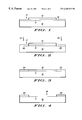
- FIGS. 1 through 4 are greatly enlarged, simplified sectional views illustrating a preferred method of patterning a substrate for further processing, in accordance with the present invention
- FIG. 5 is a greatly enlarged, simplified top elevational view of a substrate patterned for processing, in accordance with the present invention
- FIG. 6 is a greatly enlarged, simplified sectional view illustrating crystalline material selectively grown on the patterned substrate of FIG. 4, in accordance with the present invention
- FIG. 7 is a greatly enlarged, simplified sectional view illustrating crystalline material selectively grown on a facet of the crystalline material illustrated in FIG. 6, in accordance with the present invention.
- FIG. 8 is a greatly enlarged orthogonal view of a sparse-carrier device, in accordance with the present invention.
- FIG. 9 is a greatly enlarged, simplified top elevational view of another substrate patterned for processing, in accordance with the present invention.
- FIG. 10 is a greatly enlarged, simplified top elevational view of a yet still another substrate patterned for processing, in accordance with the present invention.
- FIGS. 1-4 illustrate several steps in a preferred method of masking a gallium arsenide substrate 10 for the fabrication of sparse carrier devices. While the present masking method is utilized because of its convenience (the substrate does not have to be removed from the growth chamber throughout the operation), other masking methods known in the semiconductor art may be utilized, if desired. It should be understood that gallium arsenide substrate 10 is utilized herein for purposes of this description, but other III-V compounds and other semiconductor materials may be utilized in other applications. Referring specifically to FIG. 1, a simplified sectional view of gallium arsenide substrate 10 having a surface 11 is illustrated. It should be understood that substrate 10 might simply be a supporting structure, such as a wafer or the like, or it might include various layers (not shown) formed on or in the supporting structure.
- Surface 11 of gallium arsenide substrate 10 has a film 12 (generally 20 ⁇ or less) of a native oxide which, as is well known in the art, forms substantially instantaneously upon exposure to air.
- the native oxide is not necessary to the present invention and is only illustrated because it is generally present and requires special procedures to prevent.
- various types of passivation may be used to prevent the formation of film 12 , in which case such passivation may have to be removed before the present procedure can be performed. It has been found that the present technique will operate generally as described with the surface simply being clean (i.e., no foreign matter).
- a mask 15 is positioned adjacent to surface 11 of substrate 10 for patterning surface 11 , as will be explained presently.
- Mask 15 generally is a shadow or metal mask but, in some special applications, it can be formed in the well known manner with photolithography as in an aligner or stepper (generally includes a projected image from a mask).
- photolithography and the like are not necessary for the described masking operations.
- mask 15 is a mask plate with metal lines and other features, for example, a chrome mask.
- mask 15 is positioned adjacent surface 11 so as to defined one or more growth areas or openings 16 on surface 11 beneath mask 15 and one or more unmasked portions 17 on surface 11 of substrate 10 .
- Unmasked portions 17 of surface 11 are exposed to a bright light preferably including deep ultraviolet, represented by arrows 21 in FIG. 2 .
- the bright light may be, for example, the type typically used in aligners, steppers, or E-beam devices in the semiconductor industry.
- the term deep ultraviolet refers to light in the ultraviolet range, generally with a wavelength in the range of 180 to 250 nanometers (nm). It is believed that exposure to other wavelengths, such as 248 nm in a specific example, modifies the composition of the surface oxide by forming a different kind of oxide or complex oxide molecules that are more stable than the native oxide.
- the exposure to light can be performed under a lamp.
- gallium arsenide wafer 10 with layer 12 of native oxide on the surface was provided. Standard bright lights, both at 185 nm and at 248 nm, were used with the wafer being exposed through a chrome coated mask for 5 minutes. Oxide film 20 with a thickness less than approximately 2 nm was produced in the unmasked areas.
- oxide film 20 is grown, mask 15 is removed to expose growth areas or openings 16 , as illustrated substantially in FIG. 3 .
- Oxide film 20 then serves as a mask for further process operations, such as growth, etching, and so on, and can be easily removed in situ by heating, if necessary.
- substrate 10 is then introduced into a growth chamber (not shown) and heated to a temperature of approximately 580° C. to desorb any native oxide that may still be present in growth area 16 as illustrated in FIG. 4 .
- selective growth of crystalline, or semiconductor, material 25 in growth area 16 is performed, as illustrated in FIG. 6 .
- oxide film 20 in place as a mask for further growth, a predetermined amount of crystalline material 25 is selectively grown in area (or areas) 16 .
- selective growth or selectively grown is defined as growing only in the specific or designated area 16 .
- GaAs is grown using selective area epitaxy (SAE) and well defined crystallographic facets develop while no growth occurs on oxide film 20 .
- SAE selective area epitaxy
- growth rates and shapes are crystalographically dependent, i.e., the rate and shape of growth are dependent upon the type of material 25 being utilized.
- growth area 16 may be geometrically defined to have not only a predetermined length, but also one or more predetermined widths prior to material 25 deposition.
- growth area 16 as defined by mask 15 , includes a length L, a first width A formed along substantially the entire length of growth area 16 , and a substantially centrally disposed second width B defined by an extension 40 .
- first width A is greater than second width B.
- first width A of growth area 16 is approximately 1 micron wide and may extend lengthwise (into and out-of the figure) as far as described, and second width B is somewhat greater than 1 micron wide (shown only in FIG. 5 ).
- Gallium arsenide is grown on exposed surface 11 of substrate 10 by chemical beam epitaxy using tri-isopropylgallium and arsine as the source materials.
- tri-isopropylgallium is used because it allows for lower growth temperatures that are more compatible with the resistless oxide film 20 .
- Other possible processes include, for example, the use of triethylgallium and arsine on a nitride patterned substrate at a substrate temperature of approximately 620° C.
- the crystalline structure illustrated in FIG. 6 is grown with an upper facet 26 having a first width W 1 of, in a specific example, approximately 200 nm to correspond with first width A, and a second width W 2 somewhat greater than 200 nm to correspond with second width B as shown in FIG. 8 .
- Two other facets 27 and 28 , connecting facet 26 to the substrate, are also grown but, as will be explained, not used.
- the limits on the widths W 1 and W 2 of facet 26 are related to the quantum dot diameter and desired density.
- the lower limit for width W 1 is equal to a quantum dot diameter
- the lower limit of width W 2 is equal to a plurality (such as at least two) of quantum dot diameters.
- Both the quantum dot diameter and the density are influenced by the growth conditions. It should be noted that too much material 25 (i.e., crystalline growth) results in a peak (no upper facet 26 ) and too little material 25 results in too wide a facet 26 at widths W 1 and W 2 . Further, in this specific embodiment, the crystalline structure is arranged so that upper facet 26 is the (100) facet of the GaAs. It is expected that other facets and/or facets directed other than upwardly, may be used in other applications and the present embodiment-is utilized only for the purposes of explanation.
- distance A is 1 micron. As material 25 is grown, it is reduced to approximately 0.1 micron as side or connecting facets 27 and 28 develop. Width B is achieved by forming extension 40 in the desired location of approximately 0.1 micron in width. As material 25 is grown, width A is reduced to width W 1 (0.1 micron). Width B includes width A with the additional extension 40 formed adjacent thereto. Distance B is reduced by the reduction of distance A to W 1 (0.1 micron) plus the additional width of extension 40 . The additional width of extension 40 is not decreased by the growth of material 25 due to the crystallographic orientation. In other words, the material of extension 40 grows parallel to facet 27 (the angle of the facet remains fixed), and therefore maintains its original width. Thus a small change in the difference between distance A and B results in a relatively large change in the difference between W 1 and W 2 .
- crystal material utilized in this specific application produces crystallographic facets generally as shown in the figures, it will be understood by those skilled in the art that other crystalline structures or combinations of crystalline structures can be grown and utilized.
- crystalline structures in which the outer facets grow perpendicular to the surface of the substrate, or facets which grow at a negative angle (i.e. the upper surface becomes larger than the interface at the substrate), could also be utilized.
- a second crystalline material is selectively grown on facet 26 of crystal material 25 .
- indium arsenide was selectively grown using trimethyl indium and arsine in a chemical beam epitaxy.
- the growth rates of InAs are different on the various GaAs facets and, utilizing this fact, InAs grows only on the (100) facet thick enough for strain-induced islanding to occur and a quantum structure herein referred to as a quantum dot 30 is produced.
- Quantum dot 30 is a small particle of material, e.g., semiconductor material, that is small enough to be quantum confined in three dimensions. That is, quantum dot 30 has a diameter, D, that is less that about 200 ⁇ .
- Indium arsenide growth on facets 27 and 28 is either too slow or non-existent so that no strain-induced islanding can occur on these facets.
- the ability to avoid InAs growth on oxide layer 20 and the amount of InAs that nucleates on other facets (e.g., facets 27 and 28 ) are strongly dependent on the growth conditions.
- the temperature of the substrate was lowered to approximately 525° C. and, using trimethylindium as the source, indium was delivered onto facet 26 together with arsine in a multiple of cycles each lasting 6-10 seconds long. While a multiple cycle process was used in this example, it should be understood that a continuous deposition can be utilized if desired.
- the fluxes on In and As delivered in each cycle were equivalent to that which would provide the growth of a fraction of a monolayer (ML) of In As on an unpatterned wafer. The flux levels and the total number of cycles thus determine the total amounts delivered to facet 26 .
- ML monolayer
- the flux levels and the total number of cycles thus determine the total amounts delivered to facet 26 .
- only arsine was delivered to facet 26 to allow the surface to approach equilibrium conditions.
- the diameter D is typically 30 nm or less with a height of approximately 7-8 nm.
- the quantum dots are formed with a specific distribution pattern.
- the term distribution pattern includes size of dots, density of the dots (e.g. approximately 10 9 -10 10 quantum dots/cm 2 ), position, etc. Deposition of additional mismatched material results in coalescence of individual quantum dots and formation of dislocations.
- the formation of the quantum dots on an unlimited surface occurs in a generally random location.
- the quantum dot distribution pattern for given growth conditions is, to a large extent, a function of the facet width.
- the areal density of the quantum dots decreases with the facet width.
- the rate of decrease in the quantum dot density is relatively high as the facet width is decreased but slows for facets less than approximately 1.5 m wide.
- a row of quantum dots 30 approximately one quantum dot wide and a plurality of quantum dots long may be produced along the length of facet 26 at W 1
- a plurality of rows of quantum dots 30 approximately one quantum dot wide and a plurality of quantum dots long may be produced along the length of facet 26 at W 2 , as illustrated in FIG. 8 .
- a row more than one quantum dot wide, or more than one row may be grown at W 1 of facet 26 , and even more so, by comparison, at W 2 of facet 26 if so desired in accordance with the present teachings.
- electrons introduced at one end of the quantum dots 30 will migrate or tunnel to the opposite end of the proper potentials are applied. While electrons are the prime carrier in this example, it is expected that structures utilizing holes as the carriers could also be fabricated using the precepts described herein. Also, in some approaches, no carriers travel down the chain, only polarization states change and the effect propagates along the chain. By patterning the oxide (see FIGS. 1-4) to form desired paths and structures, various sparse-carrier devices can be fabricated.
- the relative size and densities (distribution pattern) of quantum dots may be correspondingly controlled to vary along a predetermined length thereof for the manufacture of varying types of sparse-carrier devices.
- FIGS. 9 and 10 illustrate specifically masked growth areas 16 ′ and 16 ′′.
- growth area 16 ′ is formed with a substrate 10 having a length L′, a first width A′ and a second greater width B′ defined by a pair of substantially opposing extensions 41 and 42 .
- a row of quantum dots 30 approximately one quantum dot wide and a plurality of quantum dots long may be produced along a length of facet of a crystal structure grown therein to correspond with width A′
- a plurality of rows of quantum dots 30 approximately one quantum dot wide and a plurality of quantum dots long may be produced along the length of a facet of a crystal structure grown therein to correspond with width B′.
- a row more than one quantum dot wide, or more than one row may be grown on a facet to correspond with width A′ and even more so, by comparison, to correspond with width B′ if so desired.
- growth area 16 ′′ formed with a substrate 10 having a length L′′, a first width A′′ and a second lesser width B′′ defined by a pair of substantially opposing notches 43 and 44 .
- a one or more rows of quantum dots 30 approximately one quantum dot wide and a plurality of quantum dots long may be produced along a length of facet of a crystal structure grown therein to correspond with width A′′, and only one row of quantum dots 30 approximately one quantum dot wide and a plurality of quantum dots long may be produced along the length of a facet of a crystal structure grown therein to correspond with width B′′.
- width B′′ may be of an extent such that after growth of a crystalline structure at 16 ′′, the resulting facet will be too narrow for one or more quantum dots to grow.
- deposition of InAs on a selectively formed facet of another material, such as GaAs forms quantum dots selectively on the facet.
- the distribution pattern of the quantum dots not only depends on the growth conditions, but also on the size and shape of the facet.
- facet width varies, which may be controlled prior to material deposition in one or more growth areas, from very wide to narrow
- the quantum dot distribution pattern varies from zero to multiple quantum dots (many rows) to fewer rows as the facet width decreases to a single row of well separated quantum dots.
- quantum dot distribution can thus be controlled to fabricate a large variety of novel and useful device structures.
- a very narrow facet width may have all quantum dots connected, and a comparatively wide facet width may have comparatively discreet quantum dots.
Landscapes
- Engineering & Computer Science (AREA)
- Microelectronics & Electronic Packaging (AREA)
- Power Engineering (AREA)
- Physics & Mathematics (AREA)
- Condensed Matter Physics & Semiconductors (AREA)
- General Physics & Mathematics (AREA)
- Computer Hardware Design (AREA)
- Chemical & Material Sciences (AREA)
- Manufacturing & Machinery (AREA)
- Nanotechnology (AREA)
- Crystallography & Structural Chemistry (AREA)
- Materials Engineering (AREA)
- Ceramic Engineering (AREA)
- Mathematical Physics (AREA)
- Theoretical Computer Science (AREA)
- Recrystallisation Techniques (AREA)
Abstract
Description
Claims (14)
Priority Applications (1)
| Application Number | Priority Date | Filing Date | Title |
|---|---|---|---|
| US09/036,947 US6265329B1 (en) | 1998-03-09 | 1998-03-09 | Quantum deposition distribution control |
Applications Claiming Priority (1)
| Application Number | Priority Date | Filing Date | Title |
|---|---|---|---|
| US09/036,947 US6265329B1 (en) | 1998-03-09 | 1998-03-09 | Quantum deposition distribution control |
Publications (1)
| Publication Number | Publication Date |
|---|---|
| US6265329B1 true US6265329B1 (en) | 2001-07-24 |
Family
ID=21891584
Family Applications (1)
| Application Number | Title | Priority Date | Filing Date |
|---|---|---|---|
| US09/036,947 Expired - Lifetime US6265329B1 (en) | 1998-03-09 | 1998-03-09 | Quantum deposition distribution control |
Country Status (1)
| Country | Link |
|---|---|
| US (1) | US6265329B1 (en) |
Cited By (3)
| Publication number | Priority date | Publication date | Assignee | Title |
|---|---|---|---|---|
| EP1739728A1 (en) * | 2004-04-13 | 2007-01-03 | Kwansei Gakuin Educational Foundation | Method of three-dimensional microfabrication and high-density three-dimensional fine structure |
| US20080246022A1 (en) * | 2004-10-12 | 2008-10-09 | Commissariat A L'energie Atomique | Method for Producing Planar Transporting Resonance Heterostructures |
| CN107919266A (en) * | 2016-10-08 | 2018-04-17 | 中国科学院苏州纳米技术与纳米仿生研究所 | A kind of production method of quantum-dot structure |
Citations (8)
| Publication number | Priority date | Publication date | Assignee | Title |
|---|---|---|---|---|
| EP0588062A1 (en) * | 1992-08-13 | 1994-03-23 | Sony Corporation | Quantum Device and its Manufacturing Method |
| US5614435A (en) * | 1994-10-27 | 1997-03-25 | The Regents Of The University Of California | Quantum dot fabrication process using strained epitaxial growth |
| US5783840A (en) * | 1991-12-20 | 1998-07-21 | Texas Instruments Incorporated | Universal quantum dot logic cell |
| JPH10289998A (en) * | 1997-04-11 | 1998-10-27 | Motorola Inc | Lean carrier device and manufacture |
| US5831294A (en) * | 1993-09-30 | 1998-11-03 | Sony Corporation | Quantum box structure and carrier conductivity modulating device |
| US5888885A (en) * | 1997-05-14 | 1999-03-30 | Lucent Technologies Inc. | Method for fabricating three-dimensional quantum dot arrays and resulting products |
| US5905273A (en) * | 1996-12-12 | 1999-05-18 | Sony Corporation | Quantum box information storage device |
| US6244530B1 (en) * | 1996-07-17 | 2001-06-12 | Fuji Photo Film Co., Ltd. | Paper magazine for recording paper roll and recording paper roll |
-
1998
- 1998-03-09 US US09/036,947 patent/US6265329B1/en not_active Expired - Lifetime
Patent Citations (9)
| Publication number | Priority date | Publication date | Assignee | Title |
|---|---|---|---|---|
| US5783840A (en) * | 1991-12-20 | 1998-07-21 | Texas Instruments Incorporated | Universal quantum dot logic cell |
| EP0588062A1 (en) * | 1992-08-13 | 1994-03-23 | Sony Corporation | Quantum Device and its Manufacturing Method |
| US5831294A (en) * | 1993-09-30 | 1998-11-03 | Sony Corporation | Quantum box structure and carrier conductivity modulating device |
| US6020605A (en) * | 1993-09-30 | 2000-02-01 | Sony Corporation | Quantum box structure and carrier conductivity modulating device |
| US5614435A (en) * | 1994-10-27 | 1997-03-25 | The Regents Of The University Of California | Quantum dot fabrication process using strained epitaxial growth |
| US6244530B1 (en) * | 1996-07-17 | 2001-06-12 | Fuji Photo Film Co., Ltd. | Paper magazine for recording paper roll and recording paper roll |
| US5905273A (en) * | 1996-12-12 | 1999-05-18 | Sony Corporation | Quantum box information storage device |
| JPH10289998A (en) * | 1997-04-11 | 1998-10-27 | Motorola Inc | Lean carrier device and manufacture |
| US5888885A (en) * | 1997-05-14 | 1999-03-30 | Lucent Technologies Inc. | Method for fabricating three-dimensional quantum dot arrays and resulting products |
Non-Patent Citations (1)
| Title |
|---|
| "Positioning of InAs Quantum Dots on Sub-250 Facets using Selective Area Epitaxy", Tsui, p. 531-534, 1998, IEEE Journal of Quantum Electronics. * |
Cited By (6)
| Publication number | Priority date | Publication date | Assignee | Title |
|---|---|---|---|---|
| EP1739728A1 (en) * | 2004-04-13 | 2007-01-03 | Kwansei Gakuin Educational Foundation | Method of three-dimensional microfabrication and high-density three-dimensional fine structure |
| EP1739728A4 (en) * | 2004-04-13 | 2011-06-22 | Riber | Method of three-dimensional microfabrication and high-density three-dimensional fine structure |
| US20080246022A1 (en) * | 2004-10-12 | 2008-10-09 | Commissariat A L'energie Atomique | Method for Producing Planar Transporting Resonance Heterostructures |
| US8193525B2 (en) * | 2004-10-12 | 2012-06-05 | Commissariat A L'energie Atomique | Method for producing planar transporting resonance heterostructures |
| CN107919266A (en) * | 2016-10-08 | 2018-04-17 | 中国科学院苏州纳米技术与纳米仿生研究所 | A kind of production method of quantum-dot structure |
| CN107919266B (en) * | 2016-10-08 | 2020-04-10 | 青岛翼晨镭硕科技有限公司 | Manufacturing method of quantum dot structure |
Similar Documents
| Publication | Publication Date | Title |
|---|---|---|
| US8785226B2 (en) | Epitaxial growth of in-plane nanowires and nanowire devices | |
| JP2923753B2 (en) | Method for forming group III atomic layer | |
| Ishikawa et al. | Site control of self-organized InAs dots on GaAs substrates by in situ electron-beam lithography and molecular-beam epitaxy | |
| Haraguchi et al. | Self‐organized fabrication of planar GaAs nanowhisker arrays | |
| US7122827B2 (en) | Monolithic light emitting devices based on wide bandgap semiconductor nanostructures and methods for making same | |
| JP4701161B2 (en) | Precisely positioned nanowhiskers and nanowhisker arrays and methods of making them | |
| US20070257264A1 (en) | CATALYST-FREE GROWTH OF GaN NANOSCALE NEEDLES AND APPLICATION IN InGaN/GaN VISIBLE LEDS | |
| US7666696B2 (en) | Process for controlling indium clustering in ingan leds using strain arrays | |
| KR100249774B1 (en) | Growing method of high quality gaas quantum dots | |
| Kohmoto et al. | Site-controlled self-organization of InAs quantum dots | |
| US5258326A (en) | Quantum device fabrication method | |
| US6265329B1 (en) | Quantum deposition distribution control | |
| US6211530B1 (en) | Sparse-carrier devices and method of fabrication | |
| US6452205B2 (en) | Sparse-carrier devices and method of fabrication | |
| JPH10289998A (en) | Lean carrier device and manufacture | |
| JPH02188912A (en) | Selective growth method of iii-v compound semiconductor | |
| Zhang et al. | Spatially selective formation of InAs self-organized quantum dots on patterned GaAs (100) substrates | |
| KR101026507B1 (en) | Method of three-dimensional microfabrication and high-density three-dimensional fine structure | |
| JP3098371B2 (en) | Semiconductor crystal growth method | |
| JP2000124441A (en) | Preparation of semiconductor quantum dot | |
| KR20010054538A (en) | fabrication method of semiconductor device for growth of self-aligned array of self-assembled quantum dots and current blocking structure | |
| JP2004281954A (en) | Method of manufacturing quantum dot | |
| JPH10261785A (en) | Quantum box semiconductor device and its manufacture | |
| SE1930280A1 (en) | Crystal phase tuned super-structures based on nanowires | |
| Kohmoto et al. | InAs-dot/GaAs structures site-controlled by in situ EB lithography and self-organizing MBE growth |
Legal Events
| Date | Code | Title | Description |
|---|---|---|---|
| AS | Assignment |
Owner name: MOTOROLA, INC., ILLINOIS Free format text: ASSIGNMENT OF ASSIGNORS INTEREST;ASSIGNORS:SHIRALAGI, KUMAR;TSUI, RAYMOND K.;REEL/FRAME:009076/0165 Effective date: 19980309 |
|
| STCF | Information on status: patent grant |
Free format text: PATENTED CASE |
|
| AS | Assignment |
Owner name: FREESCALE SEMICONDUCTOR, INC., TEXAS Free format text: ASSIGNMENT OF ASSIGNORS INTEREST;ASSIGNOR:MOTOROLA, INC.;REEL/FRAME:015698/0657 Effective date: 20040404 Owner name: FREESCALE SEMICONDUCTOR, INC.,TEXAS Free format text: ASSIGNMENT OF ASSIGNORS INTEREST;ASSIGNOR:MOTOROLA, INC.;REEL/FRAME:015698/0657 Effective date: 20040404 |
|
| FPAY | Fee payment |
Year of fee payment: 4 |
|
| AS | Assignment |
Owner name: CITIBANK, N.A. AS COLLATERAL AGENT, NEW YORK Free format text: SECURITY AGREEMENT;ASSIGNORS:FREESCALE SEMICONDUCTOR, INC.;FREESCALE ACQUISITION CORPORATION;FREESCALE ACQUISITION HOLDINGS CORP.;AND OTHERS;REEL/FRAME:018855/0129 Effective date: 20061201 Owner name: CITIBANK, N.A. AS COLLATERAL AGENT,NEW YORK Free format text: SECURITY AGREEMENT;ASSIGNORS:FREESCALE SEMICONDUCTOR, INC.;FREESCALE ACQUISITION CORPORATION;FREESCALE ACQUISITION HOLDINGS CORP.;AND OTHERS;REEL/FRAME:018855/0129 Effective date: 20061201 |
|
| FPAY | Fee payment |
Year of fee payment: 8 |
|
| AS | Assignment |
Owner name: CITIBANK, N.A., AS COLLATERAL AGENT,NEW YORK Free format text: SECURITY AGREEMENT;ASSIGNOR:FREESCALE SEMICONDUCTOR, INC.;REEL/FRAME:024397/0001 Effective date: 20100413 Owner name: CITIBANK, N.A., AS COLLATERAL AGENT, NEW YORK Free format text: SECURITY AGREEMENT;ASSIGNOR:FREESCALE SEMICONDUCTOR, INC.;REEL/FRAME:024397/0001 Effective date: 20100413 |
|
| FPAY | Fee payment |
Year of fee payment: 12 |
|
| AS | Assignment |
Owner name: CITIBANK, N.A., AS NOTES COLLATERAL AGENT, NEW YOR Free format text: SECURITY AGREEMENT;ASSIGNOR:FREESCALE SEMICONDUCTOR, INC.;REEL/FRAME:030633/0424 Effective date: 20130521 |
|
| AS | Assignment |
Owner name: CITIBANK, N.A., AS NOTES COLLATERAL AGENT, NEW YOR Free format text: SECURITY AGREEMENT;ASSIGNOR:FREESCALE SEMICONDUCTOR, INC.;REEL/FRAME:031591/0266 Effective date: 20131101 |
|
| AS | Assignment |
Owner name: FREESCALE SEMICONDUCTOR, INC., TEXAS Free format text: PATENT RELEASE;ASSIGNOR:CITIBANK, N.A., AS COLLATERAL AGENT;REEL/FRAME:037356/0553 Effective date: 20151207 Owner name: FREESCALE SEMICONDUCTOR, INC., TEXAS Free format text: PATENT RELEASE;ASSIGNOR:CITIBANK, N.A., AS COLLATERAL AGENT;REEL/FRAME:037356/0143 Effective date: 20151207 Owner name: FREESCALE SEMICONDUCTOR, INC., TEXAS Free format text: PATENT RELEASE;ASSIGNOR:CITIBANK, N.A., AS COLLATERAL AGENT;REEL/FRAME:037354/0225 Effective date: 20151207 |
|
| AS | Assignment |
Owner name: MORGAN STANLEY SENIOR FUNDING, INC., MARYLAND Free format text: ASSIGNMENT AND ASSUMPTION OF SECURITY INTEREST IN PATENTS;ASSIGNOR:CITIBANK, N.A.;REEL/FRAME:037486/0517 Effective date: 20151207 |
|
| AS | Assignment |
Owner name: MORGAN STANLEY SENIOR FUNDING, INC., MARYLAND Free format text: ASSIGNMENT AND ASSUMPTION OF SECURITY INTEREST IN PATENTS;ASSIGNOR:CITIBANK, N.A.;REEL/FRAME:037518/0292 Effective date: 20151207 |
|
| AS | Assignment |
Owner name: MORGAN STANLEY SENIOR FUNDING, INC., MARYLAND Free format text: SUPPLEMENT TO THE SECURITY AGREEMENT;ASSIGNOR:FREESCALE SEMICONDUCTOR, INC.;REEL/FRAME:039138/0001 Effective date: 20160525 |
|
| AS | Assignment |
Owner name: NXP, B.V., F/K/A FREESCALE SEMICONDUCTOR, INC., NETHERLANDS Free format text: RELEASE BY SECURED PARTY;ASSIGNOR:MORGAN STANLEY SENIOR FUNDING, INC.;REEL/FRAME:040925/0001 Effective date: 20160912 Owner name: NXP, B.V., F/K/A FREESCALE SEMICONDUCTOR, INC., NE Free format text: RELEASE BY SECURED PARTY;ASSIGNOR:MORGAN STANLEY SENIOR FUNDING, INC.;REEL/FRAME:040925/0001 Effective date: 20160912 |
|
| AS | Assignment |
Owner name: NXP B.V., NETHERLANDS Free format text: RELEASE BY SECURED PARTY;ASSIGNOR:MORGAN STANLEY SENIOR FUNDING, INC.;REEL/FRAME:040928/0001 Effective date: 20160622 |
|
| AS | Assignment |
Owner name: NXP USA, INC., TEXAS Free format text: MERGER;ASSIGNOR:FREESCALE SEMICONDUCTOR, INC.;REEL/FRAME:041144/0363 Effective date: 20161107 |
|
| AS | Assignment |
Owner name: MORGAN STANLEY SENIOR FUNDING, INC., MARYLAND Free format text: CORRECTIVE ASSIGNMENT TO CORRECT THE REMOVE PATENTS 8108266 AND 8062324 AND REPLACE THEM WITH 6108266 AND 8060324 PREVIOUSLY RECORDED ON REEL 037518 FRAME 0292. ASSIGNOR(S) HEREBY CONFIRMS THE ASSIGNMENT AND ASSUMPTION OF SECURITY INTEREST IN PATENTS;ASSIGNOR:CITIBANK, N.A.;REEL/FRAME:041703/0536 Effective date: 20151207 |
|
| AS | Assignment |
Owner name: SHENZHEN XINGUODU TECHNOLOGY CO., LTD., CHINA Free format text: CORRECTIVE ASSIGNMENT TO CORRECT THE TO CORRECT THE APPLICATION NO. FROM 13,883,290 TO 13,833,290 PREVIOUSLY RECORDED ON REEL 041703 FRAME 0536. ASSIGNOR(S) HEREBY CONFIRMS THE THE ASSIGNMENT AND ASSUMPTION OF SECURITYINTEREST IN PATENTS.;ASSIGNOR:MORGAN STANLEY SENIOR FUNDING, INC.;REEL/FRAME:048734/0001 Effective date: 20190217 |
|
| AS | Assignment |
Owner name: NXP B.V., NETHERLANDS Free format text: RELEASE BY SECURED PARTY;ASSIGNOR:MORGAN STANLEY SENIOR FUNDING, INC.;REEL/FRAME:050744/0097 Effective date: 20190903 |
|
| AS | Assignment |
Owner name: MORGAN STANLEY SENIOR FUNDING, INC., MARYLAND Free format text: CORRECTIVE ASSIGNMENT TO CORRECT THE REMOVE APPLICATION11759915 AND REPLACE IT WITH APPLICATION 11759935 PREVIOUSLY RECORDED ON REEL 037486 FRAME 0517. ASSIGNOR(S) HEREBY CONFIRMS THE ASSIGNMENT AND ASSUMPTION OF SECURITYINTEREST IN PATENTS;ASSIGNOR:CITIBANK, N.A.;REEL/FRAME:053547/0421 Effective date: 20151207 |
|
| AS | Assignment |
Owner name: NXP B.V., NETHERLANDS Free format text: CORRECTIVE ASSIGNMENT TO CORRECT THE REMOVEAPPLICATION 11759915 AND REPLACE IT WITH APPLICATION11759935 PREVIOUSLY RECORDED ON REEL 040928 FRAME 0001. ASSIGNOR(S) HEREBY CONFIRMS THE RELEASE OF SECURITYINTEREST;ASSIGNOR:MORGAN STANLEY SENIOR FUNDING, INC.;REEL/FRAME:052915/0001 Effective date: 20160622 |
|
| AS | Assignment |
Owner name: NXP, B.V. F/K/A FREESCALE SEMICONDUCTOR, INC., NETHERLANDS Free format text: CORRECTIVE ASSIGNMENT TO CORRECT THE REMOVEAPPLICATION 11759915 AND REPLACE IT WITH APPLICATION11759935 PREVIOUSLY RECORDED ON REEL 040925 FRAME 0001. ASSIGNOR(S) HEREBY CONFIRMS THE RELEASE OF SECURITYINTEREST;ASSIGNOR:MORGAN STANLEY SENIOR FUNDING, INC.;REEL/FRAME:052917/0001 Effective date: 20160912 |