US6231666B1 - Process for forming epitaxial perovskite thin film layers using halide precursors - Google Patents
Process for forming epitaxial perovskite thin film layers using halide precursors Download PDFInfo
- Publication number
- US6231666B1 US6231666B1 US09/356,810 US35681099A US6231666B1 US 6231666 B1 US6231666 B1 US 6231666B1 US 35681099 A US35681099 A US 35681099A US 6231666 B1 US6231666 B1 US 6231666B1
- Authority
- US
- United States
- Prior art keywords
- substrate
- thin film
- perovskite
- organic salt
- titanium
- Prior art date
- Legal status (The legal status is an assumption and is not a legal conclusion. Google has not performed a legal analysis and makes no representation as to the accuracy of the status listed.)
- Expired - Lifetime
Links
Images
Classifications
-
- C—CHEMISTRY; METALLURGY
- C30—CRYSTAL GROWTH
- C30B—SINGLE-CRYSTAL GROWTH; UNIDIRECTIONAL SOLIDIFICATION OF EUTECTIC MATERIAL OR UNIDIRECTIONAL DEMIXING OF EUTECTOID MATERIAL; REFINING BY ZONE-MELTING OF MATERIAL; PRODUCTION OF A HOMOGENEOUS POLYCRYSTALLINE MATERIAL WITH DEFINED STRUCTURE; SINGLE CRYSTALS OR HOMOGENEOUS POLYCRYSTALLINE MATERIAL WITH DEFINED STRUCTURE; AFTER-TREATMENT OF SINGLE CRYSTALS OR A HOMOGENEOUS POLYCRYSTALLINE MATERIAL WITH DEFINED STRUCTURE; APPARATUS THEREFOR
- C30B29/00—Single crystals or homogeneous polycrystalline material with defined structure characterised by the material or by their shape
- C30B29/10—Inorganic compounds or compositions
- C30B29/16—Oxides
- C30B29/22—Complex oxides
- C30B29/225—Complex oxides based on rare earth copper oxides, e.g. high T-superconductors
-
- C—CHEMISTRY; METALLURGY
- C30—CRYSTAL GROWTH
- C30B—SINGLE-CRYSTAL GROWTH; UNIDIRECTIONAL SOLIDIFICATION OF EUTECTIC MATERIAL OR UNIDIRECTIONAL DEMIXING OF EUTECTOID MATERIAL; REFINING BY ZONE-MELTING OF MATERIAL; PRODUCTION OF A HOMOGENEOUS POLYCRYSTALLINE MATERIAL WITH DEFINED STRUCTURE; SINGLE CRYSTALS OR HOMOGENEOUS POLYCRYSTALLINE MATERIAL WITH DEFINED STRUCTURE; AFTER-TREATMENT OF SINGLE CRYSTALS OR A HOMOGENEOUS POLYCRYSTALLINE MATERIAL WITH DEFINED STRUCTURE; APPARATUS THEREFOR
- C30B7/00—Single-crystal growth from solutions using solvents which are liquid at normal temperature, e.g. aqueous solutions
- C30B7/005—Epitaxial layer growth
-
- H—ELECTRICITY
- H10—SEMICONDUCTOR DEVICES; ELECTRIC SOLID-STATE DEVICES NOT OTHERWISE PROVIDED FOR
- H10N—ELECTRIC SOLID-STATE DEVICES NOT OTHERWISE PROVIDED FOR
- H10N60/00—Superconducting devices
- H10N60/01—Manufacture or treatment
- H10N60/0268—Manufacture or treatment of devices comprising copper oxide
- H10N60/0296—Processes for depositing or forming copper oxide superconductor layers
- H10N60/0576—Processes for depositing or forming copper oxide superconductor layers characterised by the substrate
- H10N60/0632—Intermediate layers, e.g. for growth control
Definitions
- YBa 2 CuO 7 ⁇ x YBCO
- YBCO YBa 2 CuO 7 ⁇ x
- Production of such films likely requires use of a substrate with a similar atomic lattice structure to template crystalline growth.
- Through cold-rolling of nickel wire, long lengths of (200) oriented nickel tape have been demonstrated by Oak Ridge National Laboratory and others, enabling the required length scales of lattice-matched, oriented, and relatively inexpensive substrates.
- Superconducting materials such as YBCO would react chemically if deposited directly on nickel. Therefore, some sort of buffer layer is necessary between the YBCO and the nickel substrate.
- Ni electrodes are much less costly than the silver, silver/palladium, or platinum electrodes normally used for these applications. As electrode costs in half the expense for such capacitors, such an advance is significant.
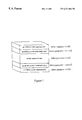
- FIG. 1 is an isometric diagram of an idealized cross section of a central substrate of oriented Ni tape on which perovskite buffer layers have been grown on which in turn have been grown YBCO layers.
- the buffer layer prevents reaction of the YBCO with the underlying Ni substrate but maintains the atomic registry of the oriented Ni substrate to allow epitaxial structures of YBCO(100)//ABO 3 (100)//Ni(100), where ABO 3 denotes a generic perovskite structure oxide buffer layer.
- ABO 3 denotes a generic perovskite structure oxide buffer layer.
- the same technique may be used for any oxide buffer layer that has similar lattice match to the top superconductor layer and nickel underlayer. As mentioned above, a continuous process is desirable for production of kilometer lengths of wire or tape.
- buffer layers of BaTiO 3 and SrTiO 3 were deposited atop the Ni by a fluorinated CSD process.
- BaTiO 3 and SrTiO 3 typically form via BaCO 3 and SrCO 3 intermediate carbonate phases, which decompose slowly and generally yield polycrystalline (non-epitaxial) films.
- Ba, Sr, and most of the other Column I alkali and Column II alkaline earth metals form carbonate phases upon exposure to CO 2 in the atmosphere or CO 2 resulting from decomposition of alcohols or other organics (e.g. Ba+CH 3 OH+3/2 O 2 ⁇ BaCO 3 +2H 2 O).
- This solution is then dip- or spin-coated onto nickel or single crystal oxide substrates to form films of 30-100 nm thickness.
- the films are heated to 100° C. on a hot plate, then to 400° C. in an inert gas (Ar, N 2 or N 2 H 2 ) atmosphere together with water vapor or H 2 , and finally to 700-800° C. in a dry inert gas (Ar, N 2 ) atmosphere.
- This process produced epitaxial films of BaTiO 3 and SrTiO 3 on Ni, without evidence of Ni oxidation which would disrupt epitaxial growth.
- Rapid heat treatment of spin-coated coated Ba acetate/Ti isopropoxide/TFA films on single crystal MgO (100) substrates produced epitaxial (100) oriented BaTiO 3 films as well.
- epitaxial BaTiO 3 films are observed immediately upon heating a film from 400° C. to 800° C. It is understood that the formation of epitaxial films in enable by formation of a liquid Ba phase at around 730° C., as indicated by the Ba-BaF 2 phase diagram.
- the perovskite metal oxides should be able to be extended beyond Ba and Sr to the rest of the column I alkali metals and column II alkaline earth metals as well as at least some of the rare earth metals such as Nd and Er.
- Ni oxidizes in the presence of O 2 or H 2 O at high temperature (>400° C.). Such oxidation is to be avoided, since formation of such a randomly oriented NiO layer atop Ni would result in the inability to template epitaxial oxide films on the Ni.
- fluorinated buffer layer precursors herein, the use of a dry N 2 or Ar atmosphere above 400° C. was found to be effective in avoiding formation of NiO, thus enable deposition of BaTiO 3 on top of the Ni.
- Presence of H 2 O above 400° C. was found to lead to formation of NiO on the randomly oriented Ni substrates, while use of dry atmospheres avoided this problem.
- a wet atmosphere was used below 400° C.
- epitaxial YBCO was deposited by CSD on BaTiO 3 //MgO and SrTiO 3 //LaAIO 3 structures. This demonstrates that Ni or single crystal substrates can be used to template CSD epitaxial perovskite layers such as BaTiO 3 and SrTiO 3 and that these perovskite layers can be successfully overgrown with epitaxial YBCO.
- TFA- and other halide-based precursors enables avoidance of alkali and alkaline earth carbonate phases in a wide variety of ceramic/perovskite thin films.
- the low temperatures (400-800° C.) used in this process enable integration of perovskite oxides with materials such as Ni without oxidation of such base-metal electrodes.
- rare earth metal oxides may be included along with the Ti oxide as part of the perovskite thin film.
- Er or Nd are include in concentrations if the 1000's of ppm range, light amplification within the layer may be possible.
- the perovskite layer is the functional layer, rather than a buffer layer.
- a perovskite film such as BaTiO 3 can serve as an epitaxial optical waveguide or in other applications.
Landscapes
- Chemical & Material Sciences (AREA)
- Engineering & Computer Science (AREA)
- Crystallography & Structural Chemistry (AREA)
- Materials Engineering (AREA)
- Metallurgy (AREA)
- Organic Chemistry (AREA)
- Inorganic Chemistry (AREA)
- Manufacturing & Machinery (AREA)
- Crystals, And After-Treatments Of Crystals (AREA)
Abstract
Description
Claims (27)
Priority Applications (1)
| Application Number | Priority Date | Filing Date | Title |
|---|---|---|---|
| US09/356,810 US6231666B1 (en) | 1999-07-20 | 1999-07-20 | Process for forming epitaxial perovskite thin film layers using halide precursors |
Applications Claiming Priority (1)
| Application Number | Priority Date | Filing Date | Title |
|---|---|---|---|
| US09/356,810 US6231666B1 (en) | 1999-07-20 | 1999-07-20 | Process for forming epitaxial perovskite thin film layers using halide precursors |
Publications (1)
| Publication Number | Publication Date |
|---|---|
| US6231666B1 true US6231666B1 (en) | 2001-05-15 |
Family
ID=23403044
Family Applications (1)
| Application Number | Title | Priority Date | Filing Date |
|---|---|---|---|
| US09/356,810 Expired - Lifetime US6231666B1 (en) | 1999-07-20 | 1999-07-20 | Process for forming epitaxial perovskite thin film layers using halide precursors |
Country Status (1)
| Country | Link |
|---|---|
| US (1) | US6231666B1 (en) |
Cited By (7)
| Publication number | Priority date | Publication date | Assignee | Title |
|---|---|---|---|---|
| US20030127051A1 (en) * | 2001-07-31 | 2003-07-10 | Fritzemeier Leslie G. | Superconductor methods and reactors |
| US20070031312A1 (en) * | 2005-08-05 | 2007-02-08 | Payne David A | Manganite perovskite ceramics, their precursors and methods for forming |
| US20080293576A1 (en) * | 2007-05-24 | 2008-11-27 | Zenergy Power Gmbh | Substrate for a Superconducting Thin-Film Strip Conductor |
| US20090246361A1 (en) * | 2008-03-31 | 2009-10-01 | Tdk Corporation | Method for manufacturing dielectric element |
| WO2015184197A3 (en) * | 2014-05-28 | 2016-03-03 | Alliance For Sustainable Energy, Llc | Methods for producing and using perovskite materials and devices therefrom |
| US9701696B2 (en) | 2015-02-27 | 2017-07-11 | Alliance For Sustainable Energy, Llc | Methods for producing single crystal mixed halide perovskites |
| US10160660B1 (en) | 2014-05-28 | 2018-12-25 | National Technology & Engineering Solutions Of Sandia, Llc | Vanadium oxide for infrared coatings and methods thereof |
Citations (4)
| Publication number | Priority date | Publication date | Assignee | Title |
|---|---|---|---|---|
| US5146299A (en) * | 1990-03-02 | 1992-09-08 | Westinghouse Electric Corp. | Ferroelectric thin film material, method of deposition, and devices using same |
| US5231074A (en) * | 1990-04-17 | 1993-07-27 | Massachusetts Institute Of Technology | Preparation of highly textured oxide superconducting films from mod precursor solutions |
| US5509189A (en) * | 1993-03-10 | 1996-04-23 | Massachusetts Institute Of Technology, A Ma Corp. | Method for making an electrochemical cell |
| US5650362A (en) * | 1993-11-04 | 1997-07-22 | Fuji Xerox Co. | Oriented conductive film and process for preparing the same |
-
1999
- 1999-07-20 US US09/356,810 patent/US6231666B1/en not_active Expired - Lifetime
Patent Citations (4)
| Publication number | Priority date | Publication date | Assignee | Title |
|---|---|---|---|---|
| US5146299A (en) * | 1990-03-02 | 1992-09-08 | Westinghouse Electric Corp. | Ferroelectric thin film material, method of deposition, and devices using same |
| US5231074A (en) * | 1990-04-17 | 1993-07-27 | Massachusetts Institute Of Technology | Preparation of highly textured oxide superconducting films from mod precursor solutions |
| US5509189A (en) * | 1993-03-10 | 1996-04-23 | Massachusetts Institute Of Technology, A Ma Corp. | Method for making an electrochemical cell |
| US5650362A (en) * | 1993-11-04 | 1997-07-22 | Fuji Xerox Co. | Oriented conductive film and process for preparing the same |
Non-Patent Citations (5)
| Title |
|---|
| P. C. McIntyre, M. J. Cima, A. Roshko, Epitaxial Nucleation and Growth of Chemically Derived Ba2Ycu3O7-x Thin Films on (001) ) SrTiO3, Journal of Applied Physics 77(10), May 15, 1995. |
| Paul C. McIntyre and Michael J. Cima, Heteroepitaxial Growth of Chemically Derived ex situ Ba2Ycu3O7-x Thin Films, J. Mater Res., vol. 9, No. 9, Sep. 1994. |
| Paul C. McIntyre, Michael J. Cima, and Man Fai Ng, Metalorganic Deposition of high JcBa2Ycu3O7-x Thin Films from Trifluoroaecetate Precursors onto (100) SrTiO3, Journal of Applied Physics, 68(8), Oct. 15, 1990. |
| Paul C. McIntyre, Michael J. Cima, John A. Smith, Jr., Robert B. Hallock, Michael P. Siegal and Julia M. Phillips, Effect of Growth Conditions on the Properties and Morphology of Chemically Derived Epitaxial Thin Films of Ba2Ycu3O7-x on (001) LaAIO3, Journal of Applied Physics 71(4), Feb. 15, 1992. |
| Ronald H. Baney, Debora F. Bergstrom, and Bruce H. Justice, Metal Iodides: Novel Solution Precursors to Cuprate Superconductors, American Chemical Society, 0897-4756/92/2804-0984, 1992. |
Cited By (13)
| Publication number | Priority date | Publication date | Assignee | Title |
|---|---|---|---|---|
| US6797313B2 (en) * | 2001-07-31 | 2004-09-28 | American Superconductor Corporation | Superconductor methods and reactors |
| US20030127051A1 (en) * | 2001-07-31 | 2003-07-10 | Fritzemeier Leslie G. | Superconductor methods and reactors |
| US8974855B2 (en) | 2005-08-05 | 2015-03-10 | The United States Department Of Energy | Manganite perovskite ceramics, their precursors and methods for forming |
| US20070031312A1 (en) * | 2005-08-05 | 2007-02-08 | Payne David A | Manganite perovskite ceramics, their precursors and methods for forming |
| US20080293576A1 (en) * | 2007-05-24 | 2008-11-27 | Zenergy Power Gmbh | Substrate for a Superconducting Thin-Film Strip Conductor |
| US8513163B2 (en) * | 2007-05-24 | 2013-08-20 | Basf Se | Substrate for a superconducting thin-film strip conductor |
| US20090246361A1 (en) * | 2008-03-31 | 2009-10-01 | Tdk Corporation | Method for manufacturing dielectric element |
| WO2015184197A3 (en) * | 2014-05-28 | 2016-03-03 | Alliance For Sustainable Energy, Llc | Methods for producing and using perovskite materials and devices therefrom |
| US10160660B1 (en) | 2014-05-28 | 2018-12-25 | National Technology & Engineering Solutions Of Sandia, Llc | Vanadium oxide for infrared coatings and methods thereof |
| US10566143B2 (en) | 2014-05-28 | 2020-02-18 | Alliance For Sustainable Energy, Llc | Methods for producing and using perovskite materials and devices therefrom |
| US10889506B2 (en) | 2014-05-28 | 2021-01-12 | National Technology & Engineering Solutions Of Sandia, Llc | Vanadium oxide for infrared coatings and methods thereof |
| US11264179B2 (en) | 2014-05-28 | 2022-03-01 | Alliance For Sustainable Energy, Llc | Methods for producing and using perovskite materials and devices therefrom |
| US9701696B2 (en) | 2015-02-27 | 2017-07-11 | Alliance For Sustainable Energy, Llc | Methods for producing single crystal mixed halide perovskites |
Similar Documents
| Publication | Publication Date | Title |
|---|---|---|
| US6077344A (en) | Sol-gel deposition of buffer layers on biaxially textured metal substances | |
| CN100367525C (en) | Methods, systems and reactors for producing superconducting materials | |
| US6537689B2 (en) | Multi-layer superconductor having buffer layer with oriented termination plane | |
| KR100585417B1 (en) | Precursor solutions and methods of using the same | |
| US7902120B2 (en) | High temperature superconductors having planar magnetic flux pinning centers and methods for making the same | |
| JPH05345613A (en) | Cubic perovskite crystal structure and method for producing the crystal structure | |
| JP5736603B2 (en) | REBCO oxide superconducting thin film and manufacturing method thereof | |
| CN103548100A (en) | Superconducting thin-film material and method for manufacturing same | |
| US20100015340A1 (en) | COMPOSITIONS AND METHODS FOR THE MANUFACTURE OF RARE EARTH METAL-Ba2Cu3O7-delta THIN FILMS | |
| US5141918A (en) | Method of forming an oxide superconducting thin film of a single phase having no carbonate | |
| Araki et al. | Firing condition for entire reactions of fluorides with water vapor in metalorganic deposition method using trifluoroacetate | |
| US7985712B2 (en) | Rare earth oxide superconductor and process for producing the same | |
| EP1598871A1 (en) | Thin-film capacitative element and electronic circuit or electronic equipment including the same | |
| US7473670B2 (en) | Process for producing rare earth oxide superconductor | |
| Araki et al. | A large volume reduction and calcining profile for large-area YBa2Cu3O7− x film by metalorganic deposition using trifluoroacetates | |
| US8030247B2 (en) | Synthesizing precursor solution enabling fabricating biaxially textured buffer layers by low temperature annealing | |
| JPS63239742A (en) | Manufacturing method of thin film superconductor | |
| JPH0358488A (en) | Planar josephson element and manufacturing method of the same | |
| JPS63279527A (en) | Manufacture of superconductor device | |
| JP2013235765A (en) | Oxide superconducting wire material and method for manufacturing the same | |
| JP3186381B2 (en) | Method for producing oriented conductive thin film | |
| Benavidez et al. | Chemical method to prepare YBa2Cu3O7− x (YBCO) films by dipping onto SrTi (Nb) O3 ceramics | |
| JP2523952B2 (en) | Thin film forming method and thin film forming apparatus | |
| JPH0214827A (en) | Production of superconductive oxide layer | |
| TWI235390B (en) | Thin film capacitive element, and electronic circuit and electronic device including the same |
Legal Events
| Date | Code | Title | Description |
|---|---|---|---|
| AS | Assignment |
Owner name: SANDIA CORPORATION, NEW MEXICO Free format text: ASSIGNMENT OF ASSIGNORS INTEREST;ASSIGNORS:CLEM, PAUL G.;VOIGHT, JAMES A.;ASHLEY, CAROL S.;AND OTHERS;REEL/FRAME:010217/0292;SIGNING DATES FROM 19990720 TO 19990812 |
|
| STCF | Information on status: patent grant |
Free format text: PATENTED CASE |
|
| REMI | Maintenance fee reminder mailed | ||
| FPAY | Fee payment |
Year of fee payment: 4 |
|
| SULP | Surcharge for late payment | ||
| AS | Assignment |
Owner name: ENERGY, U.S. DEPARTMENT OF, DISTRICT OF COLUMBIA Free format text: CONFIRMATORY LICENSE;ASSIGNOR:SANDIA CORPORATION;REEL/FRAME:015918/0993 Effective date: 19990826 |
|
| FPAY | Fee payment |
Year of fee payment: 8 |
|
| FPAY | Fee payment |
Year of fee payment: 12 |
|
| AS | Assignment |
Owner name: NATIONAL TECHNOLOGY & ENGINEERING SOLUTIONS OF SAN Free format text: CHANGE OF NAME;ASSIGNOR:SANDIA CORPORATION;REEL/FRAME:043293/0702 Effective date: 20170501 |