US6229331B1 - Apparatus for and method of inspecting patterns on semiconductor integrated devices - Google Patents

Apparatus for and method of inspecting patterns on semiconductor integrated devices Download PDF

Info

Publication number
US6229331B1
US6229331B1 US09/395,264 US39526499A US6229331B1 US 6229331 B1 US6229331 B1 US 6229331B1 US 39526499 A US39526499 A US 39526499A US 6229331 B1 US6229331 B1 US 6229331B1
Authority
US
United States
Prior art keywords
pixels
pixel
strip
mean
smaller
Prior art date
Legal status (The legal status is an assumption and is not a legal conclusion. Google has not performed a legal analysis and makes no representation as to the accuracy of the status listed.)
Expired - Fee Related
Application number
US09/395,264
Inventor
Masayuki Kuwabara
Current Assignee (The listed assignees may be inaccurate. Google has not performed a legal analysis and makes no representation or warranty as to the accuracy of the list.)
Tokyo Seimitsu Co Ltd
Original Assignee
Tokyo Seimitsu Co Ltd
Priority date (The priority date is an assumption and is not a legal conclusion. Google has not performed a legal analysis and makes no representation as to the accuracy of the date listed.)
Filing date
Publication date
Application filed by Tokyo Seimitsu Co Ltd filed Critical Tokyo Seimitsu Co Ltd
Assigned to TOKYO SEIMITSU CO., LTD. reassignment TOKYO SEIMITSU CO., LTD. ASSIGNMENT OF ASSIGNORS INTEREST (SEE DOCUMENT FOR DETAILS). Assignors: KUWABARA, MASAYUKI
Application granted granted Critical
Publication of US6229331B1 publication Critical patent/US6229331B1/en
Anticipated expiration legal-status Critical
Expired - Fee Related legal-status Critical Current

Links

Images

Classifications

    • GPHYSICS
    • G01MEASURING; TESTING
    • G01RMEASURING ELECTRIC VARIABLES; MEASURING MAGNETIC VARIABLES
    • G01R31/00Arrangements for testing electric properties; Arrangements for locating electric faults; Arrangements for electrical testing characterised by what is being tested not provided for elsewhere
    • G01R31/28Testing of electronic circuits, e.g. by signal tracer
    • G01R31/302Contactless testing
    • G01R31/308Contactless testing using non-ionising electromagnetic radiation, e.g. optical radiation
    • G01R31/311Contactless testing using non-ionising electromagnetic radiation, e.g. optical radiation of integrated circuits

Definitions

  • the present invention relates to an apparatus for, and a method of, inspecting patterns on semiconductor integrated devices and, particularly, to an apparatus for, and a method of, optically or electro-optically inspecting the surfaces of semiconductor wafers and photomasks for defects.
  • An apparatus for inspecting the appearance of semiconductor integrated devices photographs two adjacent semiconductor devices or dies, compares the images of the dies pixel by pixel, and determines that one of the dies is defective if the images disagree with each other.
  • This prior art employs a photographing apparatus such as a combination of an optical microscope and TDI (time delay integration) image pickup elements.
  • the photographing apparatus continuously scans a first die, which may be a defective die, in a row direction, obtains a multivalued image of the first die, and stores the image in an image memory.
  • the photographing apparatus picks up a multivalued image of a second die, which is a reference die and is arranged adjacent to the first die, and stores the image in the image memory.
  • the apparatus reads the images frame by frame and compares the gray levels of corresponding pixels in the frames. Any pixel that provides a gray level difference above a threshold with respect to a corresponding pixel of the reference image is determined to be defective. This technique usually provides satisfactory defect detecting sensitivity in appearance inspection.
  • semiconductor devices to be inspected must exhibit less color unevenness or process noise such as metal grain caused by surface irregularities such as metal wiring.
  • process noise A location on a semiconductor device where a lot of metal grain appears scatters light to reduce light quantity entering into an object lens of a microscope, thereby lowering the gray level of a corresponding location on an image picked up from the semiconductor device.
  • the process noise is not a critical defect such as a short circuit between wires, and therefore, it is preferable not detected. If a fixed threshold is applied to an area where the process noise is present when checking a difference between the gray levels of two pixels, the process noise will be recognized as a defect, thereby lowering the defect detecting sensitivity.
  • one prior art compares two images with each other. In each of the images, the prior art defines an area of 3 ⁇ 3 pixels and calculates a mean value of the gray levels of the 9 pixels in the area as well as a difference (hereinafter referred to as a range value) between the maximum and minimum of the gray levels of the 9 pixels in the area.
  • the prior art selects a threshold for a center pixel of the area to test the difference between the two images. Namely, each pixel in the images is provided with a proper threshold according to a mean value and/or a range value that reflect the gray levels of peripheral pixels, to improve defect detecting sensitivity.
  • FIG. 15 shows an image picked up from metal wires that are formed at intervals of 0.35 ⁇ m with each wire having a width of 0.35 ⁇ m.
  • the image is made of pixels each of 0.20 ⁇ m in size.
  • the metal wires 151 to 154 are alternated with spaces 155 to 158 .
  • Numerals 1 to 10 on the left side of the image are row numbers of the pixels, and numerals 1 to 14 on the top of the image are column numbers of the pixels.
  • Each pixel is represented as (a, b) where a is a row number and b is a column number.
  • the metal wires 151 to 154 involve no metal grain.
  • the columns 3 , 7 , 10 , and 14 are entirely in the metal wires 151 to 154 , and therefore, are brightest to provide a gray level of 225 .
  • the columns 1 , 5 , 8 , and 12 are entirely in the spaces 155 to 158 , and therefore, are darkest to provide a gray level of 25 .
  • the columns 2 , 4 , 6 , 9 , 11 , and 13 involve a mixture of metal wire and space to provide a gray level that is dependent on the ratio of the metal wire and space.
  • pixels in the column 6 have each a gray level of 175
  • pixels in the column 9 a gray level of 75
  • pixels in the column 11 a gray level of 125 .
  • the gray levels of pixels in a given column are not equal to one another and vary from one to another due to process noise such as metal grain in wiring areas and boundaries between bright and dark areas. Such boundaries scatter light to further drop gray levels.
  • the prior art calculates at least a mean value or a range value of the gray levels of every 3 ⁇ 3 pixels in a given image and, according to the mean or range values calculated, divides pixels of the image into groups. Thereafter, the prior art sets a threshold for each group.
  • FIG. 16 shows mean values calculated for the pixels of the image of FIG. 15 .
  • the mean value of each pixel is calculated from the gray levels of 3 ⁇ 3 pixels with the pixel in question being at the center of the 3 ⁇ 3 pixels.
  • Mean values for the other pixels are calculated similarly.
  • this prior art employs the mean gray levels of pixels to find thresholds that cope with local conditions such as noise, darkness, and brightness, thereby improving defect detecting sensitivity.
  • FIG. 17 shows range values calculated for the pixels of the image of FIG. 15 .
  • the range value of each pixel is calculated from the difference between the maximum and minimum of the gray levels of 3 ⁇ 3 pixels with the pixel in question being at the center of the 3 ⁇ 3 pixels.
  • the pixel ( 2 , 2 ) has a range value of 200, which is calculated from the difference between a maximum of 225 and a minimum of 25 among the gray levels of 3 ⁇ 3 pixels around the pixel ( 2 , 2 ).
  • Range values for the other pixels are calculated similarly.
  • this prior art employs the range values of pixels to find thresholds that cope with local conditions such as noise, darkness, and brightness, thereby improving defect detecting sensitivity.
  • the mean values of FIG. 16 and the range values of FIG. 17 are employed to improve defect detecting sensitivity irrespective of the presence of process noise that may fluctuate the gray levels of pixels.
  • FIGS. 15 to 17 The prior art of FIGS. 15 to 17 is imperfect to distinguish spaces from wiring areas, and therefore, is unable to completely detect critical defects such as short circuits in the spaces between the wiring areas.
  • Design rules for wire widths and intervals of semiconductor devices are improving from 0.35 ⁇ m of FIG. 15 to 0.18 ⁇ m.
  • Bright-field microscopes generally provide a pixel size of about 0.20 ⁇ m as shown in FIG. 15 .
  • the pixel size corresponds to a unit image area picked up from a wafer and is equal to a resolution.
  • the 3 ⁇ 3 square area employed by the prior arts to calculate a mean value and range value is too large and covers metal wires and a space between them.
  • a calculation of a mean value of a pixel in the space in the column 5 of FIG. 16 is affected by a part of the wire in the column 4 and a part of the wire in the column 6 .
  • the same will happen in calculating the range values of FIG. 17 .
  • areas of the same nature frequently involve varying mean and range values.
  • the space in the column 5 of FIG. 16 has a mean value of 92 while the space in the column 8 has a mean value of 108. In spite of the columns 5 and 8 both being spaces, these columns have different mean values.
  • the column 5 in FIG. 17 has a range value of 150 while the column 8 has a range value of 200. Due to these variations, the prior art must employ a wide allowance of, for example, 90 to 110 for mean values and 145 to 205 for range values to define a space between metal wires.
  • the image of FIG. 15 involves no noise. Actual images involve process noise to make the gray levels of pixels in one column uneven. Namely, actual gray levels are not like the even gray levels of FIG. 15 .
  • noise levels in a space between metal wires are relatively low because the space is free from the influence of metal grain.
  • noise levels are high because there are random grain spots in the wiring area.
  • the high noise levels greatly vary the mean values and the range values. Even in areas of the same nature, the actual mean and range values vary more than those of FIGS. 16 and 17.
  • the varying mean and range values are useless to divide pixels into groups and set thresholds for the groups because the groups based on the varying mean and range values are incorrect. Thus, it is impossible to correctly detect critical defects such as short circuits. This problem is particularly serious in range values.
  • the prior art is unable to determine whether a pixel having a range value of 200 is in a space or in a metal wire, and therefore, is unable to detect critical defects with a range value of 200. In this way, the prior art is incapable of correctly distinguishing a group of pixels that are in a space from a group of pixels that are in a metal wire, and therefore, is incapable of improving defect detecting sensitivity.
  • An object of the present invention is to provide an apparatus for, and a method of, inspecting patterns on semiconductor integrated devices, capable of correctly detecting defects on the semiconductor integrated devices.
  • an aspect of the present invention provides an apparatus for inspecting patterns on semiconductor integrated devices.
  • the apparatus has an image pickup unit for scanning patterns on first and second semiconductor integrated devices to form first and second images made of pixels represented with multivalued gray levels; an image memory for storing the first and second images; a calculation unit for sequentially reading the first and second images out of the image memory strip by strip, each strip consisting of at least two consecutive pixels aligned in one of the row and the column directions, and calculating an optimum grouping operator for a target pixel contained in the strip according to the gray levels of all pixels in the strip; a grouping unit for associating each pixel with a group according to a grouping operator calculated thus for the pixel; an image difference memory for storing gray level differences between the first and second images pixel by pixel; a threshold setting unit for setting an optimum threshold for each of the groups; and a defect detecting unit for comparing the thresholds with the gray level differences pixel by pixel and detecting defects on any one of the first and second semiconductor integrated devices.
  • the calculating unit has, for each of the first and second images, a row mean filter for calculating a mean of gray levels of pixels that are aligned in the row direction and form a strip; a column mean filter for calculating a mean of gray levels of pixels that are aligned in the column direction and form a strip; a row range filter for calculating a range value that is equal to a difference between maximum and minimum gray levels of pixels that are aligned in the row direction and form a strip; a column range filter for calculating a range value that is equal to a difference between maximum and minimum gray levels of pixels that are aligned in the column direction and form a strip; a smaller mean selector for selecting a smaller one of the outputs of the row and column mean filters; and a smaller range selector for selecting a smaller one of the outputs of the row and column range filters.
  • the calculating unit further has a first selector for selecting a smaller one of the outputs of the smaller mean selectors of the first and second images; and a second selector for selecting a smaller one of the outputs of the smaller range selectors of the first and second images.
  • the outputs of the first and second selectors are used by the grouping unit to associate each pixel with a group.
  • Each of the row mean filters and row range filters is an n ⁇ 1 filter
  • each of the column mean filters and column range filters is a 1 ⁇ n filter, where n is an integer equal to or larger than 2.
  • the grouping unit has a lookup table that stores grouping operators and corresponding groups.
  • Another aspect of the present invention provides a method of inspecting patterns on semiconductor integrated devices.
  • the method includes the steps of scanning patterns on first and second semiconductor integrated devices to form first and second images made of pixels represented with multivalued gray levels; storing the first and second images into an image memory; sequentially reading the first and second images out of the image memory strip by strip, each strip consisting of at least two consecutive pixels aligned in one of row and column directions, and calculating an optimum grouping operator for a target pixel contained in the strip according to the gray levels of all pixels in the strip; associating each pixel with a group according to a grouping operator calculated thus for the pixel; storing gray level differences between the first and second images pixel by pixel into an image difference memory; setting an optimum threshold for each of the groups; and comparing the thresholds with the gray level differences pixel by pixel and detecting defects on any one of the first and second semiconductor integrated devices.
  • FIG. 1 is a block diagram showing an apparatus for inspecting patterns according to an embodiment of the present invention
  • FIG. 2 is a block diagram showing the details of an operator calculator contained in the apparatus of FIG. 1;
  • FIG. 3 is a flowchart showing a method of inspecting patterns achieved by the apparatus of FIG. 1;
  • FIG. 4A shows the gray levels of pixels in an image of a defective die
  • FIG. 4B shows the gray levels of pixels in an image of a reference die
  • FIGS. 5A and 5B show mean values provided by 1 ⁇ 3 mean filters from the images of FIGS. 4A and 4B;
  • FIGS. 6A and 6B show mean values provided by 3 ⁇ 1 mean filters from the images of FIGS. 4A and 4B;
  • FIGS. 7A and 7B show range values provided by 1 ⁇ 3 range filters from the images of FIGS. 4A and 4B;
  • FIGS. 8A and 8B show range values provided by 3 ⁇ 1 range filters from the images of FIGS. 4A and 4B;
  • FIGS. 9A and 9B show smaller values selected from the mean values of FIGS. 5A to 6 B;
  • FIGS. 10A and 10B show smaller values selected from the range values of FIGS. 7A to 8 B;
  • FIG. 11A shows smaller values selected from the mean values of FIGS. 9A and 9B;
  • FIG. 11B shows smaller values selected from the range values of FIGS. 10A and 10B;
  • FIG. 12 shows the contents of a lookup table for dividing pixels into groups
  • FIG. 13 shows pixels divided into groups according to the lookup table of FIG. 12;
  • FIG. 14 shows a differential image generated from the images of FIGS. 4A and 4B;
  • FIG. 15 shows gray levels measured on an image of an inspection object according to a prior art
  • FIG. 16 shows mean values provided by a conventional 3 ⁇ 3 mean filter from the image of FIG. 15.
  • FIG. 17 shows range values provided by a conventional 3 ⁇ 3 mean filter from the image of FIG. 15 .
  • FIG. 1 is a block diagram showing an apparatus for inspecting patterns on semiconductor integrated circuits according to an embodiment of the present invention.
  • the apparatus has an image pickup unit 2 , an image memory 4 , an operator calculator 6 , a grouping unit 8 , a threshold setter 10 , a differential image memory 12 , and a defect detector 14 .
  • the image pickup unit 2 scans patterns on first and second semiconductor integrated devices to form first and second images made of pixels represented with multivalued gray levels.
  • the first and second semiconductor integrated devices are dies arranged adjacent to each other for inspection, one being a reference die and the other a defective die.
  • the image memory 4 stores the gray levels of the pixels of the first and second images.
  • the first image 41 may be of the defective die and the second image 42 may be of the reference die.
  • the operator calculator 6 is characteristic to the present invention.
  • the operator calculator 6 sequentially reads the first and second images 41 and 42 out of the image memory 4 strip by strip. Each strip is made of a predetermined number (2 or above) of pixels consecutively aligned in a row or column direction.
  • the operator calculator 6 calculates an operator that is optimum for associating a target pixel contained in the strip with a group.
  • the operator calculator 6 has a first operator selector 61 for selecting an optimum operator for each pixel contained in the first image 41 , a second operator selector 62 for selecting an optimum operator for each pixel contained in the second image 42 , and a third operator selector 63 for selecting an optimum one of the outputs of the first and second operator selectors 61 and 62 .
  • the details of the operator calculator 6 will be explained later.
  • the grouping unit 8 divides the pixels of the first and second images into groups according to a lookup table or function that defines relationships between mean and range values and groups.
  • the threshold setter 10 sets a threshold for each group.
  • the differential image memory 12 stores gray level differences between the first and second images 41 and 42 pixel by pixel.
  • the defect detector 14 compares the optimum thresholds provided by the threshold setter 10 with the gray level differences stored in the differential image memory 12 and detects defects on any one of the first and second semiconductor integrated devices.
  • FIG. 2 is a block diagram showing the details of the operator calculator 6 .
  • the first operator selector 61 has a 1 ⁇ n mean filter 611 , an n ⁇ 1 mean filter 612 , a 1 ⁇ n range filter 613 , an n ⁇ 1 range filter 614 , a smaller mean selector 615 , and a smaller range selector 616 .
  • the second operator selector 62 has a 1 ⁇ n mean filter 621 , an n ⁇ 1 mean filter 622 , a 1 ⁇ n range filter 623 , an n ⁇ 1 range filter 624 , a smaller mean selector 625 , and a smaller range selector 626 .
  • n is an integer equal to or larger that 2.
  • the filters mentioned above are not limited to the 1 ⁇ n and n ⁇ 1 filters. As the resolution of the image pickup unit 2 increases, the filters may be m ⁇ n and n ⁇ m filters where m and n are integers each equal to or greater than 2 with m ⁇ n.
  • the third operator selector 63 has a first selector 631 and a second selector 632 .
  • FIG. 3 is a flowchart showing a pattern inspecting method achieved by the apparatus of FIGS. 1 and 2.
  • Step S 31 scans patterns on the first and second dies to form first and second images made of pixels represented with multivalued gray levels and stores the first and second images in the image memory 4 .
  • step S 32 the operator calculator 6 sequentially reads the first and second images out of the image memory 4 strip by strip.
  • Each strip consists of a predetermined number (at least 2) of pixels that are consecutive in a row or column direction.
  • the operator calculator 6 calculates an operator that is optimum for associating a target pixel in the strip with a group.
  • step S 33 the grouping unit 8 determines a group in the lookup table corresponding to the operator of each pixel.
  • step S 34 the threshold setter 10 sets a threshold for each group.
  • Step S 35 compares the thresholds with gray level differences stored in the differential image memory 12 pixel by pixel and detects defects on any one of the first and second semiconductor integrated devices.
  • the gray level differences between the first and second images are stored in the differential image memory 12 in any one of steps S 31 and S 35 .
  • the 1 ⁇ n and n ⁇ 1 filters 611 to 614 and 621 to 624 of FIG. 2 are 1 ⁇ 3 and 3 ⁇ 1 filters.
  • FIG. 4A shows the gray levels of a first image, which is of a defective die
  • FIG. 4B shows the gray levels of a second image, which is of a reference die.
  • the images of FIGS. 4A and 4B involve random noise due to metal grain in metal wiring areas.
  • the grain levels of pixels in the metal wiring areas on the defective and reference dies vary depending on the sizes of the metal grain with a maximum gray level of 225.
  • the metal grain is process noise and should not be detected as defects.
  • the defective die has a defect 40 , i.e., a short circuit in pixels ( 4 , 4 ), ( 4 , 5 ), and ( 4 , 6 ) in a space between adjacent wires.
  • the defect 40 may be a metal hair. Due to this, the grain levels of these pixels are increased from 125 to 140, from 25 to 55, and from 175 to 185.
  • the present invention is capable of not detecting the process noise in the metal wiring areas and is capable of surely detecting the defect 40 in the space.
  • the present invention employs the filters for providing strips, detects the direction of each wiring pattern, and groups spaces separately from the wiring patterns. This will be explained in detail.
  • FIGS. 5A and 5B show mean values provided by the 1 ⁇ 3 mean filters 611 and 621 from the images of FIGS. 4A and 4B.
  • Column mean values for the other pixels are calculated similarly. Pixels in the first and tenth rows have no column mean values because there are no zeroth and eleventh rows to calculate them.
  • FIGS. 6A and 6B show mean values provided by the 3 ⁇ 1 mean filters 612 and 622 from the images of FIGS. 4A and 4B.
  • Row mean values for the other pixels are calculated similarly. Pixels in the first and seventh columns have no row mean values because there are no zeroth and eighth columns to calculate them.
  • FIGS. 7A and 7B show range values provided by the 1 ⁇ 3 range filters 613 and 623 from the images of FIGS. 4A and 4B.
  • Column range values for the other pixels are calculated similarly. Pixels in the first and tenth rows have no column range values for the same reason as for the column mean values.
  • FIGS. 8A and 8B show range values provided by the 3 ⁇ 1 range filters 614 and 624 from the images of FIGS. 4A and 4B.
  • Row range values for the other pixels are calculated similarly. Pixels in the first and seventh columns have no row range values for the same reason as for the row mean values.
  • the smaller mean selector 615 selects a smaller one of the mean values of each corresponding pair of pixels of FIGS. 5A and 6A, to provide a result of FIG. 9 A.
  • a value 98 in the pixel ( 4 , 4 ) is a smaller value between 98 of the pixel ( 4 , 4 ) of FIG. 5A and 128 of the same pixel of FIG. 6 A.
  • the smaller mean selector 615 selects smaller mean values for the other pixels.
  • the smaller mean value selector 625 selects a smaller one of the mean values of each corresponding pair of pixels of FIGS. 5B and 6B, to provide a result of FIG. 9 B.
  • a value 99 in a pixel ( 4 , 4 ) is a smaller value between 113 of the pixel ( 4 , 4 ) of FIG. 5B and 99 of the same pixel of FIG. 6 B.
  • the smaller mean selector 625 selects smaller mean values for the other pixels.
  • the smaller range value selector 616 selects a smaller one of the range values of each corresponding pair of pixels of FIGS. 7A and 8A, to provide a result of FIG. 10 A.
  • a value 75 in the pixel ( 4 , 4 ) is a smaller value between 75 of the pixel ( 4 , 4 ) of FIG. 7A and 135 of the same pixel of FIG. 8 A.
  • the smaller range value selector 616 selects smaller range values for the other pixels.
  • the smaller range value selector 626 selects a smaller one of the range values of each corresponding pair of pixels of FIG. 7B and 8B, to provide a result of FIG. 10 B.
  • a value 35 in the pixel ( 4 , 4 ) is a smaller value between 35 of the pixel ( 4 , 4 ) of FIG. 7B and 122 of the same pixel of FIG. 8 B.
  • the smaller range value selector 626 selects smaller range values for the other pixels.
  • the pixels represented with the small mean values of FIGS. 9A and 9B are divided into groups according to a reference table.
  • the first selector 631 determines which of the values of the defective die and reference die must be employed. Namely, the first selector 631 selects, for each pixel, a smaller one of the mean values of FIGS. 9A and 9B and provides a result of FIG. 11 A. For example, FIG. 9A has a mean value of 98 for the pixel ( 4 , 4 ) and FIG. 9B has a mean value of 99 for the same pixel. Then, the first selector 631 selects 98 . Similarly, the first selector 631 selects smaller mean values for the other pixels.
  • the second selector 632 selects, for each pixel, a smaller one of the range values of FIGS. 10A and 10B and provides a result of FIG. 11 B.
  • FIG. 10A has a range value of 75 for the pixel ( 4 , 4 ) and FIG. 10B has a range value of 35 for the same pixel. Then, the second selector 632 selects 35. Similarly, the second selector 632 selects smaller range values for the other pixels.
  • the grouping unit 8 divides the pixels into groups by referring to the lookup table of FIG. 12 according to the smaller mean and range values.
  • the contents of the lookup table of FIG. 12 are prepared in advance so that pixels are divided into groups to achieve optimum defect detection.
  • a pixel ( 2 , 2 ) has a mean value of 75 and a range value of 0 in FIGS. 11A and 11B, and therefore, belongs to a group 2 .
  • a pixel ( 5 , 5 ) has a mean value of 25 and a range value of 0, and therefore, belongs to a group 1 .
  • all pixels are divided into groups as shown in FIG. 13 . In FIG.
  • the differential image memory 12 stores the difference between the images of the defective die of FIG. 4 A and reference die of FIG. 4 B.
  • FIG. 14 shows gray level differences of the pixels of the differential image stored in the memory 12 .
  • a gray level difference of 17 in a pixel ( 4 , 2 ) is the difference between a gray level of 75 in the same pixel in FIG. 4A and a gray level of 58 in the same pixel in FIG. 4 B.
  • the same is applicable to the other pixels.
  • a threshold for detecting a defect is set for each group.
  • any pixel belonging to the group 3 is in a range that covers mean values of greater than 80 or in a range that covers mean values of smaller than 80 and range values of greater than 15.
  • the group 3 corresponds to an area that is mostly covered by metal wires.
  • Any pixel belonging to the group 2 is in a range that covers mean values of 40 to 80 and range values of 0 to 15.
  • the group 2 corresponds to an area that contains metal wires. Accordingly, pixels belonging to the groups 2 and 3 never involve critical defects such as short circuits, and therefore, high thresholds are set for the groups 2 and 3 .
  • Any pixel belonging to the group 1 is in a range that covers mean values of 0 to 40 and range values of 0 to 15. These small mean and range values indicate a space. Namely, the group 1 corresponds to a space, and therefore, a low threshold is set for the group 1 to surely detect critical defects such as short circuits.
  • the second column belongs to the group 2 , and a threshold of, for example, 20 is set for the group 2 so that noise due to metal grain in, for example, the pixel ( 4 , 2 ) will not be detected as a defect.
  • the third, fourth, and sixth columns belong to the group 3 , and a threshold of, for example, 70 is set for the group 3 so that noise due to metal grain in, for example, the pixels ( 2 , 3 ) and ( 4 , 4 ) will not be detected as defects.
  • the fifth column belongs to the group 1 , and a threshold of, for example, 20 is set for the group 1 so that a grain level difference of 30 in the pixel ( 4 , 5 ) is detected as a defect.
  • the above embodiment prepares a lookup table in advance and determines a group for given mean and range values.
  • the present invention is not limited to this.
  • groups may be determined according to functions based on mean and range values.
  • the above embodiment employs the row and column filters to determine an optimum direction.
  • the present invention is not limited to this.
  • an inspection file to store the running direction of each pattern in advance may be employed.
  • the direction of a filter may properly be changed according to the inspection file and positional data provided by an image pickup unit, and mean and range filters appropriate for the direction are employed to divide pixels into groups.
  • the present invention is capable of correctly dividing metal wiring areas that involve noise and spaces between the metal wiring areas into separate groups, to correctly detect critical defects such as short circuits in the spaces.

Abstract

An apparatus correctly detects critical defects in spaces between wiring patterns on semiconductor integrated devices. The apparatus picks up gray level images from semiconductor dies, sequentially reads the images strip by strip, each strip consisting of pixels aligned in a row or column direction, calculates an optimum grouping operator for the strip, divides the pixels into groups according to the grouping operators, sets thresholds for the groups, compares the thresholds with gray level differences between the gray level images, and detects defects on the semiconductor dies. Also provided is a method to achieve this technique.

Description

BACKGROUND OF THE INVENTION
1. Field of the Invention
The present invention relates to an apparatus for, and a method of, inspecting patterns on semiconductor integrated devices and, particularly, to an apparatus for, and a method of, optically or electro-optically inspecting the surfaces of semiconductor wafers and photomasks for defects.
2. Description of the Related Art
An apparatus according to a prior art for inspecting the appearance of semiconductor integrated devices photographs two adjacent semiconductor devices or dies, compares the images of the dies pixel by pixel, and determines that one of the dies is defective if the images disagree with each other. This prior art employs a photographing apparatus such as a combination of an optical microscope and TDI (time delay integration) image pickup elements. The photographing apparatus continuously scans a first die, which may be a defective die, in a row direction, obtains a multivalued image of the first die, and stores the image in an image memory. Similarly, the photographing apparatus picks up a multivalued image of a second die, which is a reference die and is arranged adjacent to the first die, and stores the image in the image memory. The apparatus reads the images frame by frame and compares the gray levels of corresponding pixels in the frames. Any pixel that provides a gray level difference above a threshold with respect to a corresponding pixel of the reference image is determined to be defective. This technique usually provides satisfactory defect detecting sensitivity in appearance inspection.
Recently, however, the requirements for the defect detecting sensitivity of appearance inspection have increasing due to finer design rules for semiconductor devices. To improve the defect detecting sensitivity of an inspection apparatus, semiconductor devices to be inspected must exhibit less color unevenness or process noise such as metal grain caused by surface irregularities such as metal wiring. In practice, however, it is difficult to eliminate such process noise from semiconductor devices. A location on a semiconductor device where a lot of metal grain appears scatters light to reduce light quantity entering into an object lens of a microscope, thereby lowering the gray level of a corresponding location on an image picked up from the semiconductor device. The process noise is not a critical defect such as a short circuit between wires, and therefore, it is preferable not detected. If a fixed threshold is applied to an area where the process noise is present when checking a difference between the gray levels of two pixels, the process noise will be recognized as a defect, thereby lowering the defect detecting sensitivity.
To solve this problem, experiments have been made to set higher thresholds for brighter areas where metal wires are present and lower thresholds for dark areas between the metal wires, so that process noise such as metal grain in the metal wires may not be detected as defects and critical defects such as short circuits between the wires are surely detected. For example, one prior art compares two images with each other. In each of the images, the prior art defines an area of 3×3 pixels and calculates a mean value of the gray levels of the 9 pixels in the area as well as a difference (hereinafter referred to as a range value) between the maximum and minimum of the gray levels of the 9 pixels in the area. According to at least one of the mean value and range value, the prior art selects a threshold for a center pixel of the area to test the difference between the two images. Namely, each pixel in the images is provided with a proper threshold according to a mean value and/or a range value that reflect the gray levels of peripheral pixels, to improve defect detecting sensitivity.
This prior art will be explained in more detail with reference to FIGS. 15 to 17.
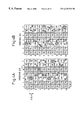
FIG. 15 shows an image picked up from metal wires that are formed at intervals of 0.35 μm with each wire having a width of 0.35 μm. The image is made of pixels each of 0.20 μm in size. The metal wires 151 to 154 are alternated with spaces 155 to 158. Numerals 1 to 10 on the left side of the image are row numbers of the pixels, and numerals 1 to 14 on the top of the image are column numbers of the pixels. Each pixel is represented as (a, b) where a is a row number and b is a column number. For the sake of simplicity of explanation, the metal wires 151 to 154 involve no metal grain. The columns 3, 7, 10, and 14 are entirely in the metal wires 151 to 154, and therefore, are brightest to provide a gray level of 225. The columns 1, 5, 8, and 12 are entirely in the spaces 155 to 158, and therefore, are darkest to provide a gray level of 25. The columns 2, 4, 6, 9, 11, and 13 involve a mixture of metal wire and space to provide a gray level that is dependent on the ratio of the metal wire and space. For example, pixels in the column 6 have each a gray level of 175, pixels in the column 9 a gray level of 75, and pixels in the column 11 a gray level of 125. In practice, the gray levels of pixels in a given column are not equal to one another and vary from one to another due to process noise such as metal grain in wiring areas and boundaries between bright and dark areas. Such boundaries scatter light to further drop gray levels.
The prior art calculates at least a mean value or a range value of the gray levels of every 3×3 pixels in a given image and, according to the mean or range values calculated, divides pixels of the image into groups. Thereafter, the prior art sets a threshold for each group.
FIG. 16 shows mean values calculated for the pixels of the image of FIG. 15. The mean value of each pixel is calculated from the gray levels of 3×3 pixels with the pixel in question being at the center of the 3×3 pixels. For example, a pixel (2, 2) has a mean value of 108, which is calculated by averaging the gray levels of 3×3 pixels around the pixel (2, 2), i.e., (25×3+75×3+225×3)/9=108.3. Mean values for the other pixels are calculated similarly. Instead of directly employing the gray levels of pixels to find thresholds, this prior art employs the mean gray levels of pixels to find thresholds that cope with local conditions such as noise, darkness, and brightness, thereby improving defect detecting sensitivity.
FIG. 17 shows range values calculated for the pixels of the image of FIG. 15. The range value of each pixel is calculated from the difference between the maximum and minimum of the gray levels of 3×3 pixels with the pixel in question being at the center of the 3×3 pixels. For example, the pixel (2, 2) has a range value of 200, which is calculated from the difference between a maximum of 225 and a minimum of 25 among the gray levels of 3×3 pixels around the pixel (2, 2). Range values for the other pixels are calculated similarly. Instead of directly employing the gray levels of pixels to find thresholds, this prior art employs the range values of pixels to find thresholds that cope with local conditions such as noise, darkness, and brightness, thereby improving defect detecting sensitivity.
Depending on the nature of an object and defects to be detected, the mean values of FIG. 16 and the range values of FIG. 17 are employed to improve defect detecting sensitivity irrespective of the presence of process noise that may fluctuate the gray levels of pixels.
It is essential for the appearance inspection apparatuses to surely detect critical defects, i.e., short circuits between metal wires. To detect such critical defects, spaces between metal wires must surely be recognized. Once the spaces are recognized, proper thresholds are set for the spaces to surely detect defects in the spaces.
The prior art of FIGS. 15 to 17 is imperfect to distinguish spaces from wiring areas, and therefore, is unable to completely detect critical defects such as short circuits in the spaces between the wiring areas.
Design rules for wire widths and intervals of semiconductor devices are improving from 0.35 μm of FIG. 15 to 0.18 μm. Bright-field microscopes generally provide a pixel size of about 0.20 μm as shown in FIG. 15. The pixel size corresponds to a unit image area picked up from a wafer and is equal to a resolution.
As the design rules become finer, the 3×3 square area employed by the prior arts to calculate a mean value and range value is too large and covers metal wires and a space between them. For example, a calculation of a mean value of a pixel in the space in the column 5 of FIG. 16 is affected by a part of the wire in the column 4 and a part of the wire in the column 6. The same will happen in calculating the range values of FIG. 17. In addition, areas of the same nature frequently involve varying mean and range values. For example, the space in the column 5 of FIG. 16 has a mean value of 92 while the space in the column 8 has a mean value of 108. In spite of the columns 5 and 8 both being spaces, these columns have different mean values. Similarly, the column 5 in FIG. 17 has a range value of 150 while the column 8 has a range value of 200. Due to these variations, the prior art must employ a wide allowance of, for example, 90 to 110 for mean values and 145 to 205 for range values to define a space between metal wires.
The image of FIG. 15 involves no noise. Actual images involve process noise to make the gray levels of pixels in one column uneven. Namely, actual gray levels are not like the even gray levels of FIG. 15.
In actual semiconductor devices, noise levels in a space between metal wires are relatively low because the space is free from the influence of metal grain. In a metal wiring area, however, noise levels are high because there are random grain spots in the wiring area. The high noise levels greatly vary the mean values and the range values. Even in areas of the same nature, the actual mean and range values vary more than those of FIGS. 16 and 17.
The varying mean and range values are useless to divide pixels into groups and set thresholds for the groups because the groups based on the varying mean and range values are incorrect. Thus, it is impossible to correctly detect critical defects such as short circuits. This problem is particularly serious in range values. The prior art is unable to determine whether a pixel having a range value of 200 is in a space or in a metal wire, and therefore, is unable to detect critical defects with a range value of 200. In this way, the prior art is incapable of correctly distinguishing a group of pixels that are in a space from a group of pixels that are in a metal wire, and therefore, is incapable of improving defect detecting sensitivity.
SUMMARY OF THE INVENTION
An object of the present invention is to provide an apparatus for, and a method of, inspecting patterns on semiconductor integrated devices, capable of correctly detecting defects on the semiconductor integrated devices.
In order to accomplish the object, an aspect of the present invention provides an apparatus for inspecting patterns on semiconductor integrated devices. The apparatus has an image pickup unit for scanning patterns on first and second semiconductor integrated devices to form first and second images made of pixels represented with multivalued gray levels; an image memory for storing the first and second images; a calculation unit for sequentially reading the first and second images out of the image memory strip by strip, each strip consisting of at least two consecutive pixels aligned in one of the row and the column directions, and calculating an optimum grouping operator for a target pixel contained in the strip according to the gray levels of all pixels in the strip; a grouping unit for associating each pixel with a group according to a grouping operator calculated thus for the pixel; an image difference memory for storing gray level differences between the first and second images pixel by pixel; a threshold setting unit for setting an optimum threshold for each of the groups; and a defect detecting unit for comparing the thresholds with the gray level differences pixel by pixel and detecting defects on any one of the first and second semiconductor integrated devices.
The calculating unit has, for each of the first and second images, a row mean filter for calculating a mean of gray levels of pixels that are aligned in the row direction and form a strip; a column mean filter for calculating a mean of gray levels of pixels that are aligned in the column direction and form a strip; a row range filter for calculating a range value that is equal to a difference between maximum and minimum gray levels of pixels that are aligned in the row direction and form a strip; a column range filter for calculating a range value that is equal to a difference between maximum and minimum gray levels of pixels that are aligned in the column direction and form a strip; a smaller mean selector for selecting a smaller one of the outputs of the row and column mean filters; and a smaller range selector for selecting a smaller one of the outputs of the row and column range filters. The calculating unit further has a first selector for selecting a smaller one of the outputs of the smaller mean selectors of the first and second images; and a second selector for selecting a smaller one of the outputs of the smaller range selectors of the first and second images. The outputs of the first and second selectors are used by the grouping unit to associate each pixel with a group.
Each of the row mean filters and row range filters is an n×1 filter, and each of the column mean filters and column range filters is a 1×n filter, where n is an integer equal to or larger than 2.
The grouping unit has a lookup table that stores grouping operators and corresponding groups.
Another aspect of the present invention provides a method of inspecting patterns on semiconductor integrated devices. The method includes the steps of scanning patterns on first and second semiconductor integrated devices to form first and second images made of pixels represented with multivalued gray levels; storing the first and second images into an image memory; sequentially reading the first and second images out of the image memory strip by strip, each strip consisting of at least two consecutive pixels aligned in one of row and column directions, and calculating an optimum grouping operator for a target pixel contained in the strip according to the gray levels of all pixels in the strip; associating each pixel with a group according to a grouping operator calculated thus for the pixel; storing gray level differences between the first and second images pixel by pixel into an image difference memory; setting an optimum threshold for each of the groups; and comparing the thresholds with the gray level differences pixel by pixel and detecting defects on any one of the first and second semiconductor integrated devices.
BRIEF DESCRIPTION OF THE DRAWINGS
Other objects and features of the present invention will be described hereinafter in detail by way of preferred embodiments with reference to the accompanying drawings, in which:
FIG. 1 is a block diagram showing an apparatus for inspecting patterns according to an embodiment of the present invention;
FIG. 2 is a block diagram showing the details of an operator calculator contained in the apparatus of FIG. 1;
FIG. 3 is a flowchart showing a method of inspecting patterns achieved by the apparatus of FIG. 1;
FIG. 4A shows the gray levels of pixels in an image of a defective die;
FIG. 4B shows the gray levels of pixels in an image of a reference die;
FIGS. 5A and 5B show mean values provided by 1×3 mean filters from the images of FIGS. 4A and 4B;
FIGS. 6A and 6B show mean values provided by 3×1 mean filters from the images of FIGS. 4A and 4B;
FIGS. 7A and 7B show range values provided by 1×3 range filters from the images of FIGS. 4A and 4B;
FIGS. 8A and 8B show range values provided by 3×1 range filters from the images of FIGS. 4A and 4B;
FIGS. 9A and 9B show smaller values selected from the mean values of FIGS. 5A to 6B;
FIGS. 10A and 10B show smaller values selected from the range values of FIGS. 7A to 8B;
FIG. 11A shows smaller values selected from the mean values of FIGS. 9A and 9B;
FIG. 11B shows smaller values selected from the range values of FIGS. 10A and 10B;
FIG. 12 shows the contents of a lookup table for dividing pixels into groups;
FIG. 13 shows pixels divided into groups according to the lookup table of FIG. 12;
FIG. 14 shows a differential image generated from the images of FIGS. 4A and 4B;
FIG. 15 shows gray levels measured on an image of an inspection object according to a prior art;
FIG. 16 shows mean values provided by a conventional 3×3 mean filter from the image of FIG. 15; and
FIG. 17 shows range values provided by a conventional 3×3 mean filter from the image of FIG. 15.
DESCRIPTION OF THE PREFERRED EMBODIMENTS
FIG. 1 is a block diagram showing an apparatus for inspecting patterns on semiconductor integrated circuits according to an embodiment of the present invention. The apparatus has an image pickup unit 2, an image memory 4, an operator calculator 6, a grouping unit 8, a threshold setter 10, a differential image memory 12, and a defect detector 14.
The image pickup unit 2 scans patterns on first and second semiconductor integrated devices to form first and second images made of pixels represented with multivalued gray levels. The first and second semiconductor integrated devices are dies arranged adjacent to each other for inspection, one being a reference die and the other a defective die.
The image memory 4 stores the gray levels of the pixels of the first and second images. The first image 41 may be of the defective die and the second image 42 may be of the reference die.
The operator calculator 6 is characteristic to the present invention. The operator calculator 6 sequentially reads the first and second images 41 and 42 out of the image memory 4 strip by strip. Each strip is made of a predetermined number (2 or above) of pixels consecutively aligned in a row or column direction. The operator calculator 6 calculates an operator that is optimum for associating a target pixel contained in the strip with a group. The operator calculator 6 has a first operator selector 61 for selecting an optimum operator for each pixel contained in the first image 41, a second operator selector 62 for selecting an optimum operator for each pixel contained in the second image 42, and a third operator selector 63 for selecting an optimum one of the outputs of the first and second operator selectors 61 and 62. The details of the operator calculator 6 will be explained later.
The grouping unit 8 divides the pixels of the first and second images into groups according to a lookup table or function that defines relationships between mean and range values and groups. The threshold setter 10 sets a threshold for each group. The differential image memory 12 stores gray level differences between the first and second images 41 and 42 pixel by pixel. The defect detector 14 compares the optimum thresholds provided by the threshold setter 10 with the gray level differences stored in the differential image memory 12 and detects defects on any one of the first and second semiconductor integrated devices.
FIG. 2 is a block diagram showing the details of the operator calculator 6. The first operator selector 61 has a 1×n mean filter 611, an n×1 mean filter 612, a 1×n range filter 613, an n×1 range filter 614, a smaller mean selector 615, and a smaller range selector 616.
The second operator selector 62 has a 1×n mean filter 621, an n×1 mean filter 622, a 1×n range filter 623, an n×1 range filter 624, a smaller mean selector 625, and a smaller range selector 626.
Here, “n” is an integer equal to or larger that 2. The filters mentioned above are not limited to the 1×n and n×1 filters. As the resolution of the image pickup unit 2 increases, the filters may be m×n and n×m filters where m and n are integers each equal to or greater than 2 with m<n.
The third operator selector 63 has a first selector 631 and a second selector 632.
FIG. 3 is a flowchart showing a pattern inspecting method achieved by the apparatus of FIGS. 1 and 2.
The method will be explained step by step.
Step S31 scans patterns on the first and second dies to form first and second images made of pixels represented with multivalued gray levels and stores the first and second images in the image memory 4.
In step S32, the operator calculator 6 sequentially reads the first and second images out of the image memory 4 strip by strip. Each strip consists of a predetermined number (at least 2) of pixels that are consecutive in a row or column direction. The operator calculator 6 calculates an operator that is optimum for associating a target pixel in the strip with a group.
In step S33, the grouping unit 8 determines a group in the lookup table corresponding to the operator of each pixel.
In step S34, the threshold setter 10 sets a threshold for each group.
Step S35 compares the thresholds with gray level differences stored in the differential image memory 12 pixel by pixel and detects defects on any one of the first and second semiconductor integrated devices.
The gray level differences between the first and second images are stored in the differential image memory 12 in any one of steps S31 and S35.
An example of the operation of the present invention will be explained with reference to FIGS. 4 to 11. In the example, the 1×n and n×1 filters 611 to 614 and 621 to 624 of FIG. 2 are 1×3 and 3×1 filters.
FIG. 4A shows the gray levels of a first image, which is of a defective die, and FIG. 4B shows the gray levels of a second image, which is of a reference die. Unlike the image shown in FIG. 15 having no noise, the images of FIGS. 4A and 4B involve random noise due to metal grain in metal wiring areas. The grain levels of pixels in the metal wiring areas on the defective and reference dies vary depending on the sizes of the metal grain with a maximum gray level of 225. The metal grain is process noise and should not be detected as defects.
The defective die has a defect 40, i.e., a short circuit in pixels (4, 4), (4, 5), and (4, 6) in a space between adjacent wires. The defect 40 may be a metal hair. Due to this, the grain levels of these pixels are increased from 125 to 140, from 25 to 55, and from 175 to 185.
The present invention is capable of not detecting the process noise in the metal wiring areas and is capable of surely detecting the defect 40 in the space.
The present invention employs the filters for providing strips, detects the direction of each wiring pattern, and groups spaces separately from the wiring patterns. This will be explained in detail.
FIGS. 5A and 5B show mean values provided by the 1×3 mean filters 611 and 621 from the images of FIGS. 4A and 4B. For example, a column mean value of 35 in a pixel (4, 5) of FIG. 5A is an average of the gray levels of a strip of 1×3 pixels consecutive to each other in a column direction with the pixel (4, 5) being at the center of the strip, i.e., (25+55+25)/3=35. Column mean values for the other pixels are calculated similarly. Pixels in the first and tenth rows have no column mean values because there are no zeroth and eleventh rows to calculate them.
FIGS. 6A and 6B show mean values provided by the 3×1 mean filters 612 and 622 from the images of FIGS. 4A and 4B. For example, a row mean value of 128 in a pixel (4, 4) of FIG. 6A is an average of the gray levels of a strip of 3×1 pixels consecutive to each other in a row direction with the pixel (4, 4) being at the center of the strip, i.e., (190+140+55)/3=128.33. Row mean values for the other pixels are calculated similarly. Pixels in the first and seventh columns have no row mean values because there are no zeroth and eighth columns to calculate them.
FIGS. 7A and 7B show range values provided by the 1×3 range filters 613 and 623 from the images of FIGS. 4A and 4B. For example, a column range value of 75 in the pixel (4, 4) of FIG. 7A is a difference between a maximum and a minimum of the gray levels of a strip of 1×3 pixels consecutive to each other in the column direction with the pixel (4, 4) being at the center of the strip, i.e., 140−65=75. Column range values for the other pixels are calculated similarly. Pixels in the first and tenth rows have no column range values for the same reason as for the column mean values.
FIGS. 8A and 8B show range values provided by the 3×1 range filters 614 and 624 from the images of FIGS. 4A and 4B. For example, a row range value of 135 in the pixel (4, 4) of FIG. 8A is a difference between a maximum and a minimum of the gray levels of a strip of 3×1 pixels consecutive to each other in the row direction with the pixel (4, 4) being at the center of the strip, i.e., 190−55=135. Row range values for the other pixels are calculated similarly. Pixels in the first and seventh columns have no row range values for the same reason as for the row mean values.
The smaller mean selector 615 selects a smaller one of the mean values of each corresponding pair of pixels of FIGS. 5A and 6A, to provide a result of FIG. 9A. In FIG. 9A, a value 98 in the pixel (4, 4) is a smaller value between 98 of the pixel (4, 4) of FIG. 5A and 128 of the same pixel of FIG. 6A. Similarly, the smaller mean selector 615 selects smaller mean values for the other pixels.
The smaller mean value selector 625 selects a smaller one of the mean values of each corresponding pair of pixels of FIGS. 5B and 6B, to provide a result of FIG. 9B. In FIG. 9B, a value 99 in a pixel (4, 4) is a smaller value between 113 of the pixel (4, 4) of FIG. 5B and 99 of the same pixel of FIG. 6B. Similarly, the smaller mean selector 625 selects smaller mean values for the other pixels.
The smaller range value selector 616 selects a smaller one of the range values of each corresponding pair of pixels of FIGS. 7A and 8A, to provide a result of FIG. 10A. In FIG. 10A, a value 75 in the pixel (4, 4) is a smaller value between 75 of the pixel (4, 4) of FIG. 7A and 135 of the same pixel of FIG. 8A. Similarly, the smaller range value selector 616 selects smaller range values for the other pixels.
The smaller range value selector 626 selects a smaller one of the range values of each corresponding pair of pixels of FIG. 7B and 8B, to provide a result of FIG. 10B. In FIG. 10B, a value 35 in the pixel (4, 4) is a smaller value between 35 of the pixel (4, 4) of FIG. 7B and 122 of the same pixel of FIG. 8B. Similarly, the smaller range value selector 626 selects smaller range values for the other pixels.
The reason why lower ones of the mean and range values of the column filters and row filters are selected as shown in FIGS. 9A to 10B is because the smaller the values the more correct the mean and range values in the column and row directions. This technique is effective when vertical and horizontal patterns change from one to another in a relatively small area as happens in logic-based semiconductor devices such as processors.
The pixels represented with the small mean values of FIGS. 9A and 9B are divided into groups according to a reference table. At this time, the first selector 631 determines which of the values of the defective die and reference die must be employed. Namely, the first selector 631 selects, for each pixel, a smaller one of the mean values of FIGS. 9A and 9B and provides a result of FIG. 11A. For example, FIG. 9A has a mean value of 98 for the pixel (4, 4) and FIG. 9B has a mean value of 99 for the same pixel. Then, the first selector 631 selects 98. Similarly, the first selector 631 selects smaller mean values for the other pixels.
The second selector 632 selects, for each pixel, a smaller one of the range values of FIGS. 10A and 10B and provides a result of FIG. 11B. For example, FIG. 10A has a range value of 75 for the pixel (4, 4) and FIG. 10B has a range value of 35 for the same pixel. Then, the second selector 632 selects 35. Similarly, the second selector 632 selects smaller range values for the other pixels.
The reason why smaller ones of the mean and range values are selected for each pixel is because selecting the smaller values improves the correctness of dividing pixels into groups to detect defects in spaces between metal wires.
The grouping unit 8 divides the pixels into groups by referring to the lookup table of FIG. 12 according to the smaller mean and range values. The contents of the lookup table of FIG. 12 are prepared in advance so that pixels are divided into groups to achieve optimum defect detection. For example, a pixel (2, 2) has a mean value of 75 and a range value of 0 in FIGS. 11A and 11B, and therefore, belongs to a group 2. A pixel (5, 5) has a mean value of 25 and a range value of 0, and therefore, belongs to a group 1. Similarly, all pixels are divided into groups as shown in FIG. 13. In FIG. 13, all pixels in the second column belong to the group 2, and all pixels in the third, fourth, and sixth columns belong to a group 3. Pixels in the fifth column belong to the group 1. Critical defects are present in spaces where mean and range values are small. By grouping the pixels, it is understood that the group 1 is a space. Accordingly, a low threshold is set only for the group 1 to surely detect defects, and higher thresholds are set for the other groups not to detect process noise due to metal grain as defects.
The differential image memory 12 stores the difference between the images of the defective die of FIG. 4A and reference die of FIG. 4B. FIG. 14 shows gray level differences of the pixels of the differential image stored in the memory 12. For example, a gray level difference of 17 in a pixel (4, 2) is the difference between a gray level of 75 in the same pixel in FIG. 4A and a gray level of 58 in the same pixel in FIG. 4B. The same is applicable to the other pixels.
A threshold for detecting a defect is set for each group. As shown in the lookup table of FIG. 12, any pixel belonging to the group 3 is in a range that covers mean values of greater than 80 or in a range that covers mean values of smaller than 80 and range values of greater than 15. The group 3 corresponds to an area that is mostly covered by metal wires. Any pixel belonging to the group 2 is in a range that covers mean values of 40 to 80 and range values of 0 to 15. The group 2 corresponds to an area that contains metal wires. Accordingly, pixels belonging to the groups 2 and 3 never involve critical defects such as short circuits, and therefore, high thresholds are set for the groups 2 and 3. Any pixel belonging to the group 1 is in a range that covers mean values of 0 to 40 and range values of 0 to 15. These small mean and range values indicate a space. Namely, the group 1 corresponds to a space, and therefore, a low threshold is set for the group 1 to surely detect critical defects such as short circuits.
In FIG. 13, the second column belongs to the group 2, and a threshold of, for example, 20 is set for the group 2 so that noise due to metal grain in, for example, the pixel (4, 2) will not be detected as a defect.
The third, fourth, and sixth columns belong to the group 3, and a threshold of, for example, 70 is set for the group 3 so that noise due to metal grain in, for example, the pixels (2, 3) and (4, 4) will not be detected as defects.
The fifth column belongs to the group 1, and a threshold of, for example, 20 is set for the group 1 so that a grain level difference of 30 in the pixel (4, 5) is detected as a defect.
The above embodiment prepares a lookup table in advance and determines a group for given mean and range values. The present invention is not limited to this. For example, groups may be determined according to functions based on mean and range values.
The above embodiment employs the row and column filters to determine an optimum direction. The present invention is not limited to this. For example, an inspection file to store the running direction of each pattern in advance may be employed. In this case, the direction of a filter may properly be changed according to the inspection file and positional data provided by an image pickup unit, and mean and range filters appropriate for the direction are employed to divide pixels into groups.
As explained above, the present invention is capable of correctly dividing metal wiring areas that involve noise and spaces between the metal wiring areas into separate groups, to correctly detect critical defects such as short circuits in the spaces.

Claims (6)

What is claimed is:
1. An apparatus for inspecting patterns on semiconductor integrated devices, comprising:
image pickup means for scanning patterns on first and second semiconductor integrated devices to form first and second images made of pixels represented with multivalued gray levels;
an image memory for storing the first and second images;
calculation means for sequentially reading the first and second images out of the image memory strip by strip, each strip consisting of at least two consecutive pixels aligned in one of row and column directions, and calculating an optimum grouping operator for a target pixel contained in the strip according to the gray levels of all pixels in the strip;
grouping means for associating each pixel with a group according to a grouping operator calculated thus for the pixel;
an image difference memory for storing gray level differences between the first and second images pixel by pixel;
threshold setting means for setting an optimum threshold for each of the groups; and
defect detecting means for comparing the thresholds with the gray level differences pixel by pixel and detecting defects on any one of the first and second semiconductor integrated devices.
2. The apparatus of claim 1, wherein:
the calculation means has, for each of the first and second images,:
a row mean filter for calculating a mean of gray levels of pixels that are aligned in the row direction and form a strip;
a column mean filter for calculating a mean of gray levels of pixels that are aligned in the column direction and form a strip;
a row range filter for calculating a range value that is equal to a difference between maximum and minimum gray levels of pixels that are aligned in the row direction and form a strip;
a column range filter for calculating a range value that is equal to a difference between maximum and minimum gray levels of pixels that are aligned in the column direction and form a strip;
smaller mean selection means for selecting a smaller one of the outputs of the row and column mean filters; and
smaller range selection means for selecting a smaller one of the outputs of the row and column range filters, the calculating means further has:
first selection means for selecting a smaller one of the outputs of the smaller mean selection means of the first and second images; and
second selection means for selecting a smaller one of the outputs of the smaller range selection means of the first and second images, the outputs of the first and second selection means being used by the grouping means to associate each pixel with a group.
3. The apparatus of claim 2, wherein:
each of the row mean filters and row range filters is an n×1 filter; and
each of the column mean filters and column range filters is a 1×n filter, where n is an integer equal to or larger than 2.
4. The apparatus of any one of claims 1 to 3, wherein:
the grouping means has a lookup table that stores grouping operators and corresponding groups.
5. A method of inspecting patterns on semiconductor integrated devices, comprising the steps of:
scanning patterns on first and second semiconductor integrated devices to form first and second images made of pixels represented with multivalued gray levels;
storing the first and second images into an image memory;
sequentially reading the first and second images out of the image memory strip by strip, each strip consisting of at least two consecutive pixels aligned in one of row and column directions, and calculating an optimum grouping operator for a target pixel contained in the strip according to the gray levels of all pixels in the strip;
associating each pixel with a group according to a grouping operator calculated thus for the pixel;
storing gray level differences between the first and second images pixel by pixel into an image difference memory;
setting an optimum threshold for each of the groups; and
comparing the thresholds with the gray level differences pixel by pixel and detecting defects on any one of the first and second semiconductor integrated devices.
6. The method of claim 5, wherein:
the sequentially reading and calculating step includes, for each of the first and second images, the steps of:
calculating, by a row mean filter, a mean of gray levels of pixels that are aligned in the row direction and form a strip;
calculating, by a column mean filter, a mean of gray levels of pixels that are aligned in the column direction and form a strip;
calculating, by a row range filter, a range value that is equal to a difference between maximum and minimum gray levels of pixels that are aligned in the row direction and form a strip;
calculating, by a column range filter, a range value that is equal to a difference between maximum and minimum gray levels of pixels that are aligned in the column direction and form a strip;
selecting, by smaller mean selection means, a smaller one of the outputs of the row and column mean filters; and
selecting, by smaller range selection means, a smaller one of the outputs of the row and column range filters, the sequentially reading and calculating step further includes the steps of:
selecting, by first selection means, a smaller one of the outputs of the smaller mean selection means of the first and second images; and
selecting, by second selection means, a smaller one of the outputs of the smaller range selection means of the first and second images, the outputs of the first and second selection means being used by the associating step to associate each pixel with a group.
US09/395,264 1998-12-02 1999-09-14 Apparatus for and method of inspecting patterns on semiconductor integrated devices Expired - Fee Related US6229331B1 (en)

Applications Claiming Priority (2)

Application Number Priority Date Filing Date Title
JP10-343220 1998-12-02
JP34322098A JP3357001B2 (en) 1998-12-02 1998-12-02 Pattern inspection apparatus and pattern inspection method for semiconductor integrated device

Publications (1)

Publication Number Publication Date
US6229331B1 true US6229331B1 (en) 2001-05-08

Family

ID=18359852

Family Applications (1)

Application Number Title Priority Date Filing Date
US09/395,264 Expired - Fee Related US6229331B1 (en) 1998-12-02 1999-09-14 Apparatus for and method of inspecting patterns on semiconductor integrated devices

Country Status (2)

Country Link
US (1) US6229331B1 (en)
JP (1) JP3357001B2 (en)

Cited By (8)

* Cited by examiner, † Cited by third party
Publication number Priority date Publication date Assignee Title
US20030095696A1 (en) * 2001-09-14 2003-05-22 Reeves Anthony P. System, method and apparatus for small pulmonary nodule computer aided diagnosis from computed tomography scans
US20030228049A1 (en) * 2002-06-11 2003-12-11 Dainippon Screen Mfg. Co., Ltd. Apparatus and method for inspecting pattern
US20040057611A1 (en) * 2002-09-23 2004-03-25 Byoung-Ho Lee Method for selecting reference images, method and apparatus for inspecting patterns on wafers, and method for dividing a wafer into application regions
US20040086168A1 (en) * 2002-10-23 2004-05-06 Masayuki Kuwabara Pattern inspection method and inspection apparatus
US20040184652A1 (en) * 2002-12-27 2004-09-23 Hideo Tsuchiya Pattern inspecting method and pattern inspecting apparatus
US20050043903A1 (en) * 2003-07-25 2005-02-24 Yasuhiko Nara Circuit-pattern inspection apparatus
US20060084262A1 (en) * 2004-10-18 2006-04-20 Shu Qin Low-k dielectric process for multilevel interconnection using microcavity engineering during electric circuit manufacture
US20190043183A1 (en) * 2017-08-01 2019-02-07 Applied Materials, Inc. Method for detecting voids and an inspection system

Families Citing this family (4)

* Cited by examiner, † Cited by third party
Publication number Priority date Publication date Assignee Title
JP2006284433A (en) * 2005-04-01 2006-10-19 Tokyo Seimitsu Co Ltd Device and method for visual examination
JP4703327B2 (en) * 2005-09-15 2011-06-15 株式会社東京精密 Image defect inspection apparatus and image defect inspection method
KR101297208B1 (en) 2011-11-04 2013-08-16 (주)오로스 테크놀로지 Defect analyzing method of semiconductor wafer
KR101297207B1 (en) 2011-11-04 2013-08-16 (주)오로스 테크놀로지 Defect analyzing method of semiconductor wafer

Citations (2)

* Cited by examiner, † Cited by third party
Publication number Priority date Publication date Assignee Title
US5469274A (en) * 1992-03-12 1995-11-21 Sharp Kabushiki Kaisha Image processing apparatus for combining differently corrected images
US5696550A (en) * 1994-07-14 1997-12-09 Advantest Corporation Image quality inspection system

Patent Citations (2)

* Cited by examiner, † Cited by third party
Publication number Priority date Publication date Assignee Title
US5469274A (en) * 1992-03-12 1995-11-21 Sharp Kabushiki Kaisha Image processing apparatus for combining differently corrected images
US5696550A (en) * 1994-07-14 1997-12-09 Advantest Corporation Image quality inspection system

Cited By (15)

* Cited by examiner, † Cited by third party
Publication number Priority date Publication date Assignee Title
US20030095696A1 (en) * 2001-09-14 2003-05-22 Reeves Anthony P. System, method and apparatus for small pulmonary nodule computer aided diagnosis from computed tomography scans
US20030228049A1 (en) * 2002-06-11 2003-12-11 Dainippon Screen Mfg. Co., Ltd. Apparatus and method for inspecting pattern
US20040057611A1 (en) * 2002-09-23 2004-03-25 Byoung-Ho Lee Method for selecting reference images, method and apparatus for inspecting patterns on wafers, and method for dividing a wafer into application regions
US7200258B2 (en) 2002-09-23 2007-04-03 Samsung Electronics Co., Ltd. Method for selecting reference images, method and apparatus for inspecting patterns on wafers, and method for dividing a wafer into application regions
US7248732B2 (en) 2002-10-23 2007-07-24 Tokyo Seimitsu Co., Ltd Pattern inspection method and inspection apparatus
US20040086168A1 (en) * 2002-10-23 2004-05-06 Masayuki Kuwabara Pattern inspection method and inspection apparatus
US20040184652A1 (en) * 2002-12-27 2004-09-23 Hideo Tsuchiya Pattern inspecting method and pattern inspecting apparatus
US7359043B2 (en) * 2002-12-27 2008-04-15 Kabushiki Kaisha Toshiba Pattern inspecting method and pattern inspecting apparatus
US7292327B2 (en) * 2003-07-25 2007-11-06 Hitachi High-Technologies Corporation Circuit-pattern inspection apparatus
US20050043903A1 (en) * 2003-07-25 2005-02-24 Yasuhiko Nara Circuit-pattern inspection apparatus
US20080174772A1 (en) * 2003-07-25 2008-07-24 Hitachi, Ltd. Circuit-pattern inspection apparatus
US7532328B2 (en) 2003-07-25 2009-05-12 Hitachi High-Technologies Corporation Circuit-pattern inspection apparatus
US20060084262A1 (en) * 2004-10-18 2006-04-20 Shu Qin Low-k dielectric process for multilevel interconnection using microcavity engineering during electric circuit manufacture
US20190043183A1 (en) * 2017-08-01 2019-02-07 Applied Materials, Inc. Method for detecting voids and an inspection system
US10922809B2 (en) * 2017-08-01 2021-02-16 Applied Materials, Inc. Method for detecting voids and an inspection system

Also Published As

Publication number Publication date
JP3357001B2 (en) 2002-12-16
JP2000171404A (en) 2000-06-23

Similar Documents

Publication Publication Date Title
US6252981B1 (en) System and method for selection of a reference die
KR100474571B1 (en) Method of setting reference images, method and apparatus using the setting method for inspecting patterns on a wafer
US7346207B2 (en) Image defect inspection method, image defect inspection apparatus, and appearance inspection apparatus
JP4776308B2 (en) Image defect inspection apparatus, image defect inspection system, defect classification apparatus, and image defect inspection method
US5204910A (en) Method for detection of defects lacking distinct edges
KR101021320B1 (en) System and method for process variation monitor
US5373147A (en) Apparatus and method for detecting line segment direction
US7492942B2 (en) Image defect inspection method, image defect inspection apparatus, and appearance inspection apparatus
US6928185B2 (en) Defect inspection method and defect inspection apparatus
US6229331B1 (en) Apparatus for and method of inspecting patterns on semiconductor integrated devices
JP4230880B2 (en) Defect inspection method
JP5660861B2 (en) Foreign matter inspection method and foreign matter inspection apparatus on substrate
US6909798B1 (en) Method of erasing repeated patterns and pattern defect inspection device
CN114972173A (en) Defect detection method, defect detection device and system
KR100827906B1 (en) Substrate inspection device
JP3870208B2 (en) Image processing method and inspection apparatus
US20060251295A1 (en) Method and device for evaluating defects in textile structures
JPH0943162A (en) External appearance inspection method
JP2001319221A (en) Method and device for inspection
JPH08193959A (en) Device and method for detecting surface scratch of inspection object
JP2008164303A (en) Imaging condition determination method for periodic pattern, defect inspection method, and defect inspecting device
JPH04294260A (en) Inspecting apparatus for printed pattern quality
JP2001210690A (en) Macroscopic inspecting apparatus for semiconductor wafer
JPH07140090A (en) Item discrimination method for appearance test
JPH0436643A (en) Tablet inspection device

Legal Events

Date Code Title Description
AS Assignment

Owner name: TOKYO SEIMITSU CO., LTD., JAPAN

Free format text: ASSIGNMENT OF ASSIGNORS INTEREST;ASSIGNOR:KUWABARA, MASAYUKI;REEL/FRAME:010253/0818

Effective date: 19990902

FPAY Fee payment

Year of fee payment: 4

FPAY Fee payment

Year of fee payment: 8

FEPP Fee payment procedure

Free format text: PAYOR NUMBER ASSIGNED (ORIGINAL EVENT CODE: ASPN); ENTITY STATUS OF PATENT OWNER: LARGE ENTITY

REMI Maintenance fee reminder mailed
LAPS Lapse for failure to pay maintenance fees
STCH Information on status: patent discontinuation

Free format text: PATENT EXPIRED DUE TO NONPAYMENT OF MAINTENANCE FEES UNDER 37 CFR 1.362

FP Lapsed due to failure to pay maintenance fee

Effective date: 20130508