US6229184B1 - Semiconductor device with a modulated gate oxide thickness - Google Patents
Semiconductor device with a modulated gate oxide thickness Download PDFInfo
- Publication number
- US6229184B1 US6229184B1 US09/250,174 US25017499A US6229184B1 US 6229184 B1 US6229184 B1 US 6229184B1 US 25017499 A US25017499 A US 25017499A US 6229184 B1 US6229184 B1 US 6229184B1
- Authority
- US
- United States
- Prior art keywords
- thickness
- dielectric layer
- substrate
- gate dielectric
- gate
- Prior art date
- Legal status (The legal status is an assumption and is not a legal conclusion. Google has not performed a legal analysis and makes no representation as to the accuracy of the status listed.)
- Expired - Lifetime
Links
Images


Classifications
-
- H10D64/01344—
-
- H10D64/01348—
-
- H—ELECTRICITY
- H10—SEMICONDUCTOR DEVICES; ELECTRIC SOLID-STATE DEVICES NOT OTHERWISE PROVIDED FOR
- H10D—INORGANIC ELECTRIC SEMICONDUCTOR DEVICES
- H10D64/00—Electrodes of devices having potential barriers
- H10D64/20—Electrodes characterised by their shapes, relative sizes or dispositions
- H10D64/27—Electrodes not carrying the current to be rectified, amplified, oscillated or switched, e.g. gates
- H10D64/311—Gate electrodes for field-effect devices
- H10D64/411—Gate electrodes for field-effect devices for FETs
- H10D64/511—Gate electrodes for field-effect devices for FETs for IGFETs
- H10D64/514—Gate electrodes for field-effect devices for FETs for IGFETs characterised by the insulating layers
- H10D64/516—Gate electrodes for field-effect devices for FETs for IGFETs characterised by the insulating layers the thicknesses being non-uniform
-
- H—ELECTRICITY
- H10—SEMICONDUCTOR DEVICES; ELECTRIC SOLID-STATE DEVICES NOT OTHERWISE PROVIDED FOR
- H10D—INORGANIC ELECTRIC SEMICONDUCTOR DEVICES
- H10D64/00—Electrodes of devices having potential barriers
- H10D64/60—Electrodes characterised by their materials
- H10D64/66—Electrodes having a conductor capacitively coupled to a semiconductor by an insulator, e.g. MIS electrodes
- H10D64/68—Electrodes having a conductor capacitively coupled to a semiconductor by an insulator, e.g. MIS electrodes characterised by the insulator, e.g. by the gate insulator
- H10D64/693—Electrodes having a conductor capacitively coupled to a semiconductor by an insulator, e.g. MIS electrodes characterised by the insulator, e.g. by the gate insulator the insulator comprising nitrogen, e.g. nitrides, oxynitrides or nitrogen-doped materials
-
- H10P30/222—
Definitions
- the present invention relates to a semiconductor device suitable for high speed performance.
- the present invention is particularly applicable for ultra large scale integration semiconductor devices having a design rule of abut 0.18 micron and under.
- An advantage of the present invention is a semiconductor device comprising a transistor exhibiting reduced drain capacitance and a gate oxide layer with high reliability.
- Another advantage of the present invention is a method of manufacturing a semiconductor device comprising a transistor with reduced drain capacitance and a gate oxide layer with high integrity.
- a semiconductor device containing a transistor comprising: a gate dielectric layer having first and second side surfaces on a substrate with a channel region therebetween; source and drain regions in the substrate with the channel region therebetween, the drain region formed proximate the first side surface and the source region formed proximate the second side surface; and a gate electrode on the gate dielectric layer, wherein the gate dielectric layer has a thickness at the first side surface which is less than its thickness at the second side surface.
- Another aspect of the present invention is a method of manufacturing a semiconductor device, the method comprising: forming a gate dielectric layer on a substrate surface, the gate dielectric layer having first and second side surfaces and a thickness at the first side surface which is less than its thickness at the second side surface; forming a gate electrode layer on the gate dielectric layer; and forming source and drain regions in the semiconductor substrate with a channel region therebetween underlying the gate dielectric layer, the drain region formed proximate the first side surface and the source region formed proximate the second side surface.
- Embodiments of the present invention include a semiconductor device comprising a transistor with a gate oxide layer having a thickness which gradually increases from proximate the drain region to proximate the source region, and a gate oxide having a first uniform thickness and a second uniform thickness greater than the first uniform thickness with a gradually increasing the transition zone between the first thickness and the second thickness.
- Embodiments of the present invention also include thermally oxidizing a substrate surface to form a gate oxide layer having a modulated thickness by ion implanting neutral impurities, such as silicon, argon or germanium, to increase the substrate surface oxidation rate proximate the contemplated source region and/or ion implanting nitrogen into the substrate surface to reduce the oxidation rate proximate the contemplated drain region.
- FIG. 1 schematically illustrates a transistor comprising a modulated gate oxide thickness in accordance with an embodiment of the present invention.
- FIG. 2 Schematically illustrates a transistor comprising a modulated gate oxide thickness in accordance with another embodiment of the present invention.
- FIGS. 3 and 4 represent sequential phases of a method in accordance with an embodiment of the present invention.
- FIGS. 5 and 6 represent sequential phases of a method in accordance with another embodiment of the present invention.
- FIGS. 7, 8 , 9 and 10 represent sequential phases of a method in accordance with further embodiment of the present invention.
- the present invention addresses and solves problems attendant upon attempting to satisfy the speed requirements for semiconductor circuitry as feature sizes are reduced into the deep sub-micron ranges to satisfy the increasing demands for miniaturization.
- the present invention enjoys particular industrial applicability in manufacturing semiconductor devices having a design rule of about 0.18 micron and under, e.g., about 0.15 micron and under.
- the present invention advantageously reduces drain capacitance without creating reliability problems attendant upon reduction of the gate dielectric layer thickness.
- the present invention achieves the foregoing objectives by strategically decoupling the thickness of the gate dielectric layer proximate the drain region from the thickness of the gate dielectric layer proximate the source region.
- the present invention provides a gate dielectric layer with a modulated thickness strategically optimized in proximity to the drain region for reducing the drain capacitance thereby increasing circuit speed.
- the thickness of the gate oxide layer is optimized proximate the source region for improved mechanical stress and reduced hot carrier injection, and furthermore decreasing the leakage current in the “OFF” state.
- a transistor is formed with a gate dielectric layer having a thickness proximate the drain region which is less than the gate dielectric layer thickness proximate the source region.
- the gate dielectric layer is formed without any step region, thereby avoiding an abrupt change or spike in the electric field.
- Embodiments of the present invention include forming a gate dielectric layer having a thickness which gradually increases from proximate the drain region to proximate the source region.
- the optimum thickness of the gate dielectric layer at the drain region and at the source region can be readily determined in a particular situation. For example, it was found suitable to form the gate dielectric layer with a thickness proximate the source region which exceeds the thickness proximate the drain region by about 10 ⁇ to about 20 ⁇ .
- Embodiments of the present invention comprise forming a gate dielectric layer having a thickness proximate the drain region of about 15 ⁇ to about 25 ⁇ and a thickness proximate the source region of about 25 ⁇ to about 35 ⁇ .
- Embodiments of the present invention further comprise forming a gate dielectric layer having a first portion of a substantially uniform first thickness of about 15 ⁇ to about 25 ⁇ proximate the drain region, a second portion of substantially uniform second thickness greater than the first thickness, i.e. about 25 ⁇ to about 35 ⁇ , proximate the source region, and a transition zone therebetween increasing in thickness from the first portion to the second portion.
- a gate electrode layer e.g. doped polycrystalline silicon
- Shallow source and drain extension implants are then formed with the shallow drain extension implant proximate the first side surface of the gate dielectric layer having the reduced thickness.
- Dielectric sidewall spacers are then formed and ion implantation conducted to form the moderate or heavily doped implants which, after subsequent conventional annealing, form source and drain regions with shallow extensions.
- the gate dielectric layer of the present invention can comprise any conventional gate dielectric material employed for a gate dielectric layer in manufacturing semiconductor devices, e.g. silicon oxide or silicon oxynitride.
- the gate dielectric layer can be formed of silicon oxide by thermal oxidation.
- Embodiments of the present invention comprise strategically altering the substrate surface to obtain a differential oxidation rate, thereby enabling forming the gate oxide layer with a modulated thickness.
- a neutral impurity such as silicon, germanium or argon
- the oxidation rate of a selected portion of the substrate is reduced, as by ion implanting nitrogen, thereby enabling formation of the gate oxide layer having a modulated thickness by thermal oxidation.
- the oxidation rate of the substrate surface is selectively increased proximate the contemplated source region and the oxidation rate selectively reduced by nitrogen implantation proximate the contemplated drain region, in either order, prior to thermal oxidation.
- inventions of the present invention comprise forming a gate oxide layer at a first thickness, selectively etching a portion of the gate oxide layer by reducing its thickness to a second thickness proximate the contemplated drain region and then thermally oxidizing, with the use of masks, to form a transition zone gradually decreasing from the first thickness to the second thicknesses, thereby avoiding abrupt stepped portions.
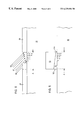
- FIG. 1 An embodiment of the present invention is schematically illustrated in FIG. 1 and comprises substrate 10 , gate dielectric layer 11 formed on the main surface of substrate 10 with a channel region 12 thereunder.
- Gate dielectric layer comprises first side surface 11 A and second side surface 11 B, and has a thickness which gradually increases from the first side surface 11 A to the second side surface 11 B.
- Gate electrode 13 is formed on gate dielectric layer 11 , and dielectric sidewall spacers 14 , e.g., silicon nitride or silicon oxynitride, are formed thereon in a conventional manner.
- Drain region comprising shallow extension 15 and a moderately or heavily doped region 16 , is formed proximate the first side surface 11 A of gate dielectric layer 11 having a reduced thickness, while source region, shallow source extension 17 and moderately or heavily region 18 , is formed proximate the second side surface 11 B of gate dielectric layer 11 .
- FIG. 2 Another embodiment of the present invention is shown in FIG. 2 wherein features similar to those of FIG. 1 are denoted by similar reference numerals.
- the embodiment schematically illustrated in FIG. 2 comprises a gate dielectric layer having a first portion 20 having a substantially uniform first thickness, a second portion 21 having a substantially uniform second thickness greater than the first thickness, and a transition zone 22 which gradually increases in thickness from the first portion 20 to the second portion 21 , thereby avoiding an abrupt stepped feature and consequential spike in the electric field.
- FIGS. 3 and 4 schematically illustrate sequential phases of methodology in accordance with an embodiment of the present invention.
- a photoresist mask 30 is formed on the main surface of substrate 10 .
- Region A denotes the contemplated channel region which is to underlie the gate oxide layer of the transistor.
- Neutral impurities atoms are then ion implanted, as shown by arrows 31 , into a selected portion of the surface of the substrate 10 , indicated by “X” marks.
- X ion implanted
- Suitable ions include silicon, germanium and argon, which cause damage to the crystalline structure of the semiconductor substrate thereby increasing its oxidation rate.
- the photoresist mask 30 is then stripped, a gate electrode layer is deposited, and patterning is conducted to form the gate electrode structure, as shown in FIG. 4, comprising gate electrode 13 overlying gate oxide layer 11 having a gradually increasing thickness in progressing from the first side surface 11 A to the second side surface 11 B.
- nitrogen atoms are ion implanted, by angular ion implantation indicated by arrows 50 , into a selected portion of the main surface of substrate 10 .
- the implanted nitrogen atoms “X” retard oxidation of the selected portion of the substrate.
- Photoresist mask 30 is then removed, thermal oxidation is conducted, gate electrode layer, e.g., doped polycrystalline silicon, is deposited and patterning is conducted to form the gate electrode structure as depicted in FIG. 6 comprising gate electrode 13 on gate oxide layer 11 having first side surface 11 A second side surface 11 B, and a thickness which gradually increases from the first side surface 11 A to the second side surface 11 B.
- an implantation dosage of about 1 ⁇ 10 12 to about 1 ⁇ 10 13 atoms cm ⁇ 2 at an energy of about 3 to about 5KeV can be employed.
- an implantation dosage of about 5 ⁇ 10 12 to about 5 ⁇ 10 13 atoms cm ⁇ 2 and an implantation energy of about 3 to about 5 KeV can be employed.
- Angular ion implantation of the neutral atoms or nitrogen can be implemented at an angle of about 30° to about 45° with respect to the substrate surface.
- FIGS. 7-10 Another embodiment of methodology in accordance with the present invention is schematically illustrated in FIGS. 7-10.
- the surface of substrate 10 is oxidized in a conventional manner to form a gate oxide layer 70 .
- Region A denotes the contemplated channel region which would underlie the ultimately formed gate oxide layer.
- a photoresist mask 71 is formed over the contemplated gate oxide layer extending from the contemplated source region toward the contemplated drain region, and etching is conducted to remove the portion of the gate oxide layer 70 extending from the contemplated source region away from the contemplated drain region.
- another photoresist mask 80 is formed overlying a portion of remaining gate oxide layer 81 (FIG.
- etching is conducted to reduce the thickness of the exposed portion of the remaining gate oxide layer, thereby leaving a second portion 92 having a thickness greater than the first portion 91 , as shown in FIG. 9.
- a hard mask 90 is then formed exposing a region adjoining the step between the first portion 91 and second portion 92 .
- Thermal oxidation is then conducted to form a transition zone 100 , as shown in FIG. 10, which gradually increases from the first portion 91 of the gate oxide layer to the second portion 92 , thereby forming a gate oxide structure having a modulated thickness similar to that shown in FIG. 2 .
- the present invention advantageously enables manufacturing a semiconductor device comprising a transistor with a gate dielectric layer having a differential thickness, wherein the thickness proximate the drain region is optimized independently of the thickness proximate the source region, thereby reducing the drain capacitance without adversely impacting the structural integrity of the gate dielectric layer or creating reliability problems.
- the present invention enjoys applicability in the manufacture of various types of semiconductor devices, and is particularly applicable in manufacturing semiconductor devices having submicron design rules, e.g, a design rule of about 0.18 microns and under, such as about 0.15 micron and under.
Landscapes
- Insulated Gate Type Field-Effect Transistor (AREA)
Abstract
Description
Claims (20)
Priority Applications (1)
| Application Number | Priority Date | Filing Date | Title |
|---|---|---|---|
| US09/250,174 US6229184B1 (en) | 1999-02-16 | 1999-02-16 | Semiconductor device with a modulated gate oxide thickness |
Applications Claiming Priority (1)
| Application Number | Priority Date | Filing Date | Title |
|---|---|---|---|
| US09/250,174 US6229184B1 (en) | 1999-02-16 | 1999-02-16 | Semiconductor device with a modulated gate oxide thickness |
Publications (1)
| Publication Number | Publication Date |
|---|---|
| US6229184B1 true US6229184B1 (en) | 2001-05-08 |
Family
ID=22946596
Family Applications (1)
| Application Number | Title | Priority Date | Filing Date |
|---|---|---|---|
| US09/250,174 Expired - Lifetime US6229184B1 (en) | 1999-02-16 | 1999-02-16 | Semiconductor device with a modulated gate oxide thickness |
Country Status (1)
| Country | Link |
|---|---|
| US (1) | US6229184B1 (en) |
Cited By (16)
| Publication number | Priority date | Publication date | Assignee | Title |
|---|---|---|---|---|
| US6348388B1 (en) * | 1999-11-30 | 2002-02-19 | International Business Machines Corporation | Process for fabricating a uniform gate oxide of a vertical transistor |
| US6514843B2 (en) * | 2001-04-27 | 2003-02-04 | International Business Machines Corporation | Method of enhanced oxidation of MOS transistor gate corners |
| US20030082861A1 (en) * | 2001-10-29 | 2003-05-01 | Nec Corporation | Method for fabricating a MOSFET |
| US20030104661A1 (en) * | 2001-02-01 | 2003-06-05 | Kazuhide Koyama | Semiconductor device and fabrication method therefor |
| US20050130441A1 (en) * | 2003-11-05 | 2005-06-16 | Geon-Ook Park | Semiconductor devices and methods of manufacturing the same |
| US20060084220A1 (en) * | 2004-10-15 | 2006-04-20 | Freescale Semiconductor, Inc. | Differentially nitrided gate dielectrics in CMOS fabrication process |
| US20070164326A1 (en) * | 2004-02-20 | 2007-07-19 | Yasuhiro Okamoto | Field effect transistor |
| US20100178754A1 (en) * | 2009-01-09 | 2010-07-15 | Samsung Electronics Co., Ltd. | Method of manufacturing cmos transistor |
| US20110097824A1 (en) * | 2009-10-22 | 2011-04-28 | International Business Machines Corporation | Method of creating an extremely thin semiconductor-on- insulator (etsoi) layer having a uniform thickness |
| US20110095366A1 (en) * | 2009-10-22 | 2011-04-28 | International Business Machines Corporation | Forming an extremely thin semiconductor-on-insulator (etsoi) layer |
| US20110095393A1 (en) * | 2009-10-22 | 2011-04-28 | International Business Machines Corporation | Creating extremely thin semiconductor-on-insulator (etsoi) having substantially uniform thickness |
| US20160268428A1 (en) * | 2005-12-22 | 2016-09-15 | Micron Technology, Inc. | Electronic device with asymmetric gate strain |
| US20170317123A1 (en) * | 2011-09-30 | 2017-11-02 | Taiwan Semiconductor Manufacturing Company, Ltd. | Methods of Manufacturing Semiconductor Devices |
| US11362188B2 (en) * | 2017-12-27 | 2022-06-14 | Intel Corporation | Field effect transistors with reduced electric field by thickening dielectric on the drain side |
| US11682726B2 (en) | 2020-12-30 | 2023-06-20 | United Microelectronics Corp. | High voltage semiconductor device and manufacturing method thereof |
| WO2025094625A1 (en) * | 2023-10-30 | 2025-05-08 | ソニーセミコンダクタソリューションズ株式会社 | Light detection apparatus, semiconductor device, and manufacturing method for semiconductor device |
Citations (2)
| Publication number | Priority date | Publication date | Assignee | Title |
|---|---|---|---|---|
| US5949117A (en) * | 1995-12-26 | 1999-09-07 | Micron Technology, Inc. | Highly efficient transistor for fast programming of flash memories |
| US6077749A (en) * | 1998-03-03 | 2000-06-20 | Advanced Micro Devices, Inc. | Method of making dual channel gate oxide thickness for MOSFET transistor design |
-
1999
- 1999-02-16 US US09/250,174 patent/US6229184B1/en not_active Expired - Lifetime
Patent Citations (2)
| Publication number | Priority date | Publication date | Assignee | Title |
|---|---|---|---|---|
| US5949117A (en) * | 1995-12-26 | 1999-09-07 | Micron Technology, Inc. | Highly efficient transistor for fast programming of flash memories |
| US6077749A (en) * | 1998-03-03 | 2000-06-20 | Advanced Micro Devices, Inc. | Method of making dual channel gate oxide thickness for MOSFET transistor design |
Cited By (32)
| Publication number | Priority date | Publication date | Assignee | Title |
|---|---|---|---|---|
| US6348388B1 (en) * | 1999-11-30 | 2002-02-19 | International Business Machines Corporation | Process for fabricating a uniform gate oxide of a vertical transistor |
| KR100839894B1 (en) | 2001-02-01 | 2008-06-20 | 소니 가부시끼 가이샤 | Semiconductor device and manufacturing method thereof |
| US20030104661A1 (en) * | 2001-02-01 | 2003-06-05 | Kazuhide Koyama | Semiconductor device and fabrication method therefor |
| US6664165B2 (en) * | 2001-02-01 | 2003-12-16 | Sony Corporation | Semiconductor device and fabrication method therefor |
| US6514843B2 (en) * | 2001-04-27 | 2003-02-04 | International Business Machines Corporation | Method of enhanced oxidation of MOS transistor gate corners |
| US20030082861A1 (en) * | 2001-10-29 | 2003-05-01 | Nec Corporation | Method for fabricating a MOSFET |
| US6713333B2 (en) * | 2001-10-29 | 2004-03-30 | Nec Electronics Corporation | Method for fabricating a MOSFET |
| US20050130441A1 (en) * | 2003-11-05 | 2005-06-16 | Geon-Ook Park | Semiconductor devices and methods of manufacturing the same |
| US7348247B2 (en) * | 2003-11-05 | 2008-03-25 | Dongbu Electronics Co., Ltd. | Semiconductor devices and methods of manufacturing the same |
| US20080191290A1 (en) * | 2003-11-05 | 2008-08-14 | Geon-Ook Park | Semiconductor devices and methods of manufacturing the same |
| US20070164326A1 (en) * | 2004-02-20 | 2007-07-19 | Yasuhiro Okamoto | Field effect transistor |
| US20060084220A1 (en) * | 2004-10-15 | 2006-04-20 | Freescale Semiconductor, Inc. | Differentially nitrided gate dielectrics in CMOS fabrication process |
| US9780184B2 (en) * | 2005-12-22 | 2017-10-03 | Micron Technology, Inc. | Electronic device with asymmetric gate strain |
| US20160268428A1 (en) * | 2005-12-22 | 2016-09-15 | Micron Technology, Inc. | Electronic device with asymmetric gate strain |
| US20100178754A1 (en) * | 2009-01-09 | 2010-07-15 | Samsung Electronics Co., Ltd. | Method of manufacturing cmos transistor |
| US8110483B2 (en) | 2009-10-22 | 2012-02-07 | International Business Machines Corporation | Forming an extremely thin semiconductor-on-insulator (ETSOI) layer |
| US20110095393A1 (en) * | 2009-10-22 | 2011-04-28 | International Business Machines Corporation | Creating extremely thin semiconductor-on-insulator (etsoi) having substantially uniform thickness |
| US8124427B2 (en) | 2009-10-22 | 2012-02-28 | International Business Machines Corporation | Method of creating an extremely thin semiconductor-on-insulator (ETSOI) layer having a uniform thickness |
| US8940554B2 (en) | 2009-10-22 | 2015-01-27 | International Business Machines Corporation | Method of creating an extremely thin semiconductor-on-insulator (ETSOI) layer having a uniform thickness |
| US9018024B2 (en) | 2009-10-22 | 2015-04-28 | International Business Machines Corporation | Creating extremely thin semiconductor-on-insulator (ETSOI) having substantially uniform thickness |
| US9263517B2 (en) | 2009-10-22 | 2016-02-16 | Globalfoundries. Inc. | Extremely thin semiconductor-on-insulator (ETSOI) layer |
| US20110095366A1 (en) * | 2009-10-22 | 2011-04-28 | International Business Machines Corporation | Forming an extremely thin semiconductor-on-insulator (etsoi) layer |
| US20110097824A1 (en) * | 2009-10-22 | 2011-04-28 | International Business Machines Corporation | Method of creating an extremely thin semiconductor-on- insulator (etsoi) layer having a uniform thickness |
| US10157942B2 (en) * | 2011-09-30 | 2018-12-18 | Taiwan Semiconductor Manufacturing Company | Semiconductor devices having reduced noise |
| US20170317123A1 (en) * | 2011-09-30 | 2017-11-02 | Taiwan Semiconductor Manufacturing Company, Ltd. | Methods of Manufacturing Semiconductor Devices |
| US10515990B2 (en) | 2011-09-30 | 2019-12-24 | Taiwan Semiconductor Manufacturing Company | Semiconductor devices having reduced noise |
| US11362188B2 (en) * | 2017-12-27 | 2022-06-14 | Intel Corporation | Field effect transistors with reduced electric field by thickening dielectric on the drain side |
| US11682726B2 (en) | 2020-12-30 | 2023-06-20 | United Microelectronics Corp. | High voltage semiconductor device and manufacturing method thereof |
| US20230335637A1 (en) * | 2020-12-30 | 2023-10-19 | United Microelectronics Corp. | Manufacturing method of high voltage semiconductor device |
| US12080794B2 (en) * | 2020-12-30 | 2024-09-03 | United Microelectronics Corp. | Manufacturing method of high voltage semiconductor device |
| US12206020B2 (en) | 2020-12-30 | 2025-01-21 | United Microelectronics Corp. | High voltage semiconductor device |
| WO2025094625A1 (en) * | 2023-10-30 | 2025-05-08 | ソニーセミコンダクタソリューションズ株式会社 | Light detection apparatus, semiconductor device, and manufacturing method for semiconductor device |
Similar Documents
| Publication | Publication Date | Title |
|---|---|---|
| US6229184B1 (en) | Semiconductor device with a modulated gate oxide thickness | |
| KR100407385B1 (en) | Dual damascene copper gate and interconnet therefore | |
| US5198378A (en) | Process of fabricating elevated source/drain transistor | |
| US6949436B2 (en) | Composite spacer liner for improved transistor performance | |
| US8084312B2 (en) | Nitrogen based implants for defect reduction in strained silicon | |
| KR20030043939A (en) | Method and device to reduce gate-induced drain leakage(GIDL) current in thin gate oxide MOSFETS | |
| US5677218A (en) | Method of fabricating FET device with narrow gate length | |
| CN1183586C (en) | Method for suppressing narrow width effects in CMOS technology | |
| US6548369B1 (en) | Multi-thickness silicon films on a single semiconductor-on-insulator (SOI) chip using simox | |
| US7148096B2 (en) | Method of manufacturing a semiconductor device having a gate electrode containing polycrystalline silicon-germanium | |
| US6503844B2 (en) | Notched gate configuration for high performance integrated circuits | |
| US5115296A (en) | Preferential oxidization self-aligned contact technology | |
| US6200887B1 (en) | Method to form a smooth gate polysilicon sidewall in the fabrication of integrated circuits | |
| US7573086B2 (en) | TaN integrated circuit (IC) capacitor | |
| EP1456888B1 (en) | Electrically programmed mos transistor source/drain series resistance | |
| US20030232473A1 (en) | Gate electrode doping method for forming semiconductor integrated circuit microelectronic fabrication with varying effective gate dielectric layer thicknesses | |
| US8034695B2 (en) | Semiconductor device and method of manufacturing the same | |
| US5811339A (en) | Method of fabricating deep submicron MOSFET with narrow gate length using thermal oxidation of polysilicon | |
| JP2001053138A (en) | Manufacture of semiconductor device | |
| US6153486A (en) | Method for establishing shallow junction in semiconductor device to minimize junction capacitance | |
| KR100252858B1 (en) | Semiconductor device and manufacturing method thereof | |
| US5937302A (en) | Method of forming lightly doped drain region and heavily doping a gate using a single implant step | |
| CN1312747C (en) | Manufacturing method of metal oxide semiconductor transistor | |
| KR100280537B1 (en) | Semiconductor device manufacturing method | |
| US20070048962A1 (en) | TaN integrated circuit (IC) capacitor formation |
Legal Events
| Date | Code | Title | Description |
|---|---|---|---|
| AS | Assignment |
Owner name: ADVANCED MICRO DEVICES, INC., CALIFORNIA Free format text: ASSIGNMENT OF ASSIGNORS INTEREST;ASSIGNOR:RICCOBENE, CONCETTA;REEL/FRAME:009774/0433 Effective date: 19990209 |
|
| STCF | Information on status: patent grant |
Free format text: PATENTED CASE |
|
| FPAY | Fee payment |
Year of fee payment: 4 |
|
| FPAY | Fee payment |
Year of fee payment: 8 |
|
| AS | Assignment |
Owner name: GLOBALFOUNDRIES INC., CAYMAN ISLANDS Free format text: AFFIRMATION OF PATENT ASSIGNMENT;ASSIGNOR:ADVANCED MICRO DEVICES, INC.;REEL/FRAME:023119/0083 Effective date: 20090630 |
|
| FPAY | Fee payment |
Year of fee payment: 12 |
|
| AS | Assignment |
Owner name: WILMINGTON TRUST, NATIONAL ASSOCIATION, DELAWARE Free format text: SECURITY AGREEMENT;ASSIGNOR:GLOBALFOUNDRIES INC.;REEL/FRAME:049490/0001 Effective date: 20181127 |
|
| AS | Assignment |
Owner name: GLOBALFOUNDRIES INC., CAYMAN ISLANDS Free format text: RELEASE BY SECURED PARTY;ASSIGNOR:WILMINGTON TRUST, NATIONAL ASSOCIATION;REEL/FRAME:054636/0001 Effective date: 20201117 |
|
| AS | Assignment |
Owner name: GLOBALFOUNDRIES U.S. INC., NEW YORK Free format text: RELEASE BY SECURED PARTY;ASSIGNOR:WILMINGTON TRUST, NATIONAL ASSOCIATION;REEL/FRAME:056987/0001 Effective date: 20201117 Owner name: GLOBALFOUNDRIES U.S. INC., NEW YORK Free format text: RELEASE OF SECURITY INTEREST;ASSIGNOR:WILMINGTON TRUST, NATIONAL ASSOCIATION;REEL/FRAME:056987/0001 Effective date: 20201117 |