US6222233B1 - Lateral RF MOS device with improved drain structure - Google Patents
Lateral RF MOS device with improved drain structure Download PDFInfo
- Publication number
- US6222233B1 US6222233B1 US09/410,934 US41093499A US6222233B1 US 6222233 B1 US6222233 B1 US 6222233B1 US 41093499 A US41093499 A US 41093499A US 6222233 B1 US6222233 B1 US 6222233B1
- Authority
- US
- United States
- Prior art keywords
- region
- lateral
- plug
- mos transistor
- semiconductor material
- Prior art date
- Legal status (The legal status is an assumption and is not a legal conclusion. Google has not performed a legal analysis and makes no representation as to the accuracy of the status listed.)
- Expired - Lifetime
Links
Images


Classifications
-
- H—ELECTRICITY
- H10—SEMICONDUCTOR DEVICES; ELECTRIC SOLID-STATE DEVICES NOT OTHERWISE PROVIDED FOR
- H10D—INORGANIC ELECTRIC SEMICONDUCTOR DEVICES
- H10D62/00—Semiconductor bodies, or regions thereof, of devices having potential barriers
- H10D62/10—Shapes, relative sizes or dispositions of the regions of the semiconductor bodies; Shapes of the semiconductor bodies
- H10D62/113—Isolations within a component, i.e. internal isolations
- H10D62/115—Dielectric isolations, e.g. air gaps
- H10D62/116—Dielectric isolations, e.g. air gaps adjoining the input or output regions of field-effect devices, e.g. adjoining source or drain regions
-
- H—ELECTRICITY
- H10—SEMICONDUCTOR DEVICES; ELECTRIC SOLID-STATE DEVICES NOT OTHERWISE PROVIDED FOR
- H10D—INORGANIC ELECTRIC SEMICONDUCTOR DEVICES
- H10D30/00—Field-effect transistors [FET]
- H10D30/60—Insulated-gate field-effect transistors [IGFET]
- H10D30/601—Insulated-gate field-effect transistors [IGFET] having lightly-doped drain or source extensions, e.g. LDD IGFETs or DDD IGFETs
- H10D30/603—Insulated-gate field-effect transistors [IGFET] having lightly-doped drain or source extensions, e.g. LDD IGFETs or DDD IGFETs having asymmetry in the channel direction, e.g. lateral high-voltage MISFETs having drain offset region or extended drain IGFETs [EDMOS]
-
- H—ELECTRICITY
- H10—SEMICONDUCTOR DEVICES; ELECTRIC SOLID-STATE DEVICES NOT OTHERWISE PROVIDED FOR
- H10D—INORGANIC ELECTRIC SEMICONDUCTOR DEVICES
- H10D64/00—Electrodes of devices having potential barriers
- H10D64/20—Electrodes characterised by their shapes, relative sizes or dispositions
- H10D64/23—Electrodes carrying the current to be rectified, amplified, oscillated or switched, e.g. sources, drains, anodes or cathodes
- H10D64/251—Source or drain electrodes for field-effect devices
- H10D64/256—Source or drain electrodes for field-effect devices for lateral devices wherein the source or drain electrodes are recessed in semiconductor bodies
-
- H—ELECTRICITY
- H10—SEMICONDUCTOR DEVICES; ELECTRIC SOLID-STATE DEVICES NOT OTHERWISE PROVIDED FOR
- H10D—INORGANIC ELECTRIC SEMICONDUCTOR DEVICES
- H10D62/00—Semiconductor bodies, or regions thereof, of devices having potential barriers
- H10D62/10—Shapes, relative sizes or dispositions of the regions of the semiconductor bodies; Shapes of the semiconductor bodies
- H10D62/13—Semiconductor regions connected to electrodes carrying current to be rectified, amplified or switched, e.g. source or drain regions
- H10D62/149—Source or drain regions of field-effect devices
- H10D62/151—Source or drain regions of field-effect devices of IGFETs
-
- H—ELECTRICITY
- H10—SEMICONDUCTOR DEVICES; ELECTRIC SOLID-STATE DEVICES NOT OTHERWISE PROVIDED FOR
- H10D—INORGANIC ELECTRIC SEMICONDUCTOR DEVICES
- H10D62/00—Semiconductor bodies, or regions thereof, of devices having potential barriers
- H10D62/10—Shapes, relative sizes or dispositions of the regions of the semiconductor bodies; Shapes of the semiconductor bodies
- H10D62/17—Semiconductor regions connected to electrodes not carrying current to be rectified, amplified or switched, e.g. channel regions
- H10D62/351—Substrate regions of field-effect devices
- H10D62/357—Substrate regions of field-effect devices of FETs
- H10D62/364—Substrate regions of field-effect devices of FETs of IGFETs
- H10D62/378—Contact regions to the substrate regions
Definitions
- the current invention is in the field of lateral RF MOS devices.
- BJT NPN bipolar junction transistor
- MOSFET vertical structures As processing technology improved, in the early 1970's a number of MOSFET vertical structures begun to challenge the dominance of the BJT at the lower RF frequencies, trading the cost of the large silicon area, necessary to provide the current capability in MOSFETs, for the cost of simple processing.
- the advantages that the MOSFET structure provided to the user were: higher power gain, ruggedness (defined as the capacity to withstand transients) and ease of biasing.
- the new prior art RF MOS devices utilize the standard lateral MOS device with a diffused via that connects the source to the backside of the chip such that the back side becomes both electrical and thermal ground.
- the prior art structure also uses a polysilicide gate process as a compromise between the fabrication benefits of the self aligned polysilicon gate and the high frequency performance of the metal gate structure.
- the prior art structure has extended the frequency of operation of MOS devices into the 2 GHz region thus covering two frequency bands of great commercial importance: the cellular and PCS/PCN mobile telephone bands.
- the via backside contact design and the polysilicide gate processing technology have allowed the prior art device to attain its performance. Firstly, by transferring the source connection to the backside of the chip through a diffused via, the packaging of the device has been simplified reducing parasitic inductance and resistance to ground. The thermal dissipation has been also improved because an electrical isolation layer in the package has been removed. Secondly, the output capacitance of RF MOS device for the common-source mode of amplification operation has been made comparable to the output capacitance obtained with BJT structures. This results in improved collector efficiency and in wider usable bandwidth (BW) of the RF MOS device operating as an amplifier.
- BW usable bandwidth
- the design of the existing lateral RF MOS devices was further improved in the lateral RF MOS device disclosed in the U.S. Pat. No. 5,949,104, issued on Sep. 7, 1999 and incorporated by reference herein in its entirety.
- the connection from the source to the backside of the silicon substrate was improved by using a metal plug.
- the usage of the metal plug to connect the source to the backside of the silicon substrate further reduced the space needed for that connection, and eliminated the lateral as well as the downward movement of the source to backside via diffusion.
- the metal plug design allowed the inclusion of more usable device active area per unit chip area, lead to an increase of available device output power per unity chip area, resulted in a further decrement of the minimal value of the drain-source capacitance (C ds ), and in a wider usable BW of the device operating as an amplifier.
- Prior art lateral RF MOS devices have an inadequate maximum density of current that could flow in the source-drain channel due to a low breakdown voltage. Indeed, dimensions of the source-drain channel are limited by the size of the lateral RF MOS device. The increased breakdown voltage would allow higher current density to flow in the source-drain channel thus increasing the power that could be dissipated at the lateral RF MOS device of the same size.
- the patent application #1 addresses the problem of inadequate maximum density of current that could flow in the source-drain channel due to a low breakdown voltage in a prior art lateral RF MOS by including two drain drift regions with different concentrations of carriers in the source-drain current channel.
- a prior art lateral RF MOS device is difficult to use as a power amplifier with sufficient bandwidth (BW) to cover the high frequencies (900 MHZ ⁇ 2 GHz) that are important for wireless applications. This is due to the fact that a prior art lateral RF MOS device has a too high output drain-source capacitance.
- the present invention provides for a lateral RF MOS device having the prior art size but a decreased drain-source capacitance.
- One aspect of the present invention is directed to a lateral MOS structure having an oxide plug in the drain region and a metal plug in the source region.
- the lateral MOS structure comprises a semiconductor material of a P-type having a first dopant concentration P ⁇ and a top surface.
- a conductive gate overlies the top surface of the semiconductor material and is insulated from it.
- a first region of a second conductivity type and having a second dopant concentration is formed completely within the semiconductor material of the first conductivity type.
- the first region forms a first enhanced drain drift region of the RF MOS transistor structure.
- the lateral MOS structure further comprises a second region of the second conductivity type and having a third dopant concentration being higher than the second dopant concentration formed in the semiconductor material.
- the second region forms a second enhanced drain drift region of the RF MOS transistor.
- the second enhanced drain drift region contacts the first enhanced drain drift region.
- the lateral MOS structure further comprises a drain region contacting the second enhanced drain drift region, a body region having a first end underlying the conductive gate, a source region located within the body region, a contact enhancement region located within the body region, a conductive plug region formed in the source region and the body region of the semiconductor material, and an oxide region formed in the drain region of the RF MOS transistor.
- the first conductivity type is of P type.
- the dopant concentration of the second enhanced drain drift region N 2 is 3/2 as much as the dopant concentration of the first enhanced drain drift N 1 .
- the lateral MOS structure comprises a semiconductor material of a P-type having a first dopant concentration P ⁇ and a top surface.
- a conductive gate overlies the top surface of the semiconductor material and is insulated from it.
- a first region of a second conductivity type and having a second dopant concentration is formed completely within the semiconductor material of the first conductivity type. The first region forms an enhanced drain drift region of the RF MOS transistor structure.
- the lateral MOS structure further comprises a drain region contacting the enhanced drain drift region, a body region having a first end underlying the conductive gate, a source region located within the body region, a contact enhancement region located within the body region, a conductive plug region formed in the source region and the body region of the semiconductor material, and an oxide region formed in the drain region of the RF MOS transistor.
- the oxide region comprises a shallow oxide plug region formed underneath the drain contact area.
- the shallow oxide plug region is located completely within the semiconductor material of the first conductivity type.
- the oxide region comprises a deep oxide plug region formed underneath the drain contact area.
- the deep oxide plug region separates a top or lateral surface of the drain region from a highly conductive substrate of the structure.
- the conductive plug region connects the source region and the body region of the semiconductor material to the backside of the MOS structure.
- the conductive plug region connects a surface of the source region and a lateral surface of the body region of the semiconductor material to a highly conductive substrate of the lateral MOS structure.
- the conductive plug can comprise: a metal plug, or a silicided plug.
- the silicided metal plug can comprise: a tungsten silicided plug, a titanium silicided plug, a cobalt silicided plug, or a platinum silicided plug.
- FIG. 1A shows an idealized NMOS device cross section with depletion and induced channel and with applied positive V GS .
- FIG. 1B is a small-signal MOS transistor equivalent circuit.
- FIG. 1C is an illustration of the prior art structure of lateral RF MOS devices.
- FIG. 1D depicts a lateral view of a simplified plug contact structure of a lateral RF MOS transistor.
- FIG. 1E depicts a detailed lateral view of the plug contact structure of a lateral RF MOS transistor.
- FIG. 2 illustrates a lateral view of a plug contact structure, wherein the conductive plug region connects a top surface and a lateral surface of the source region of the semiconductor material to a highly conductive substrate of the RF MOS structure.
- FIG. 3 is a lateral view of the MOS structure, wherein a V-shaped conductive plug region connects a top surface and a lateral surface of the source region of the semiconductor material to a backside of the MOS structure.
- FIG. 4 depicts a structure of the lateral RF MOS device having two enhanced drain drift regions.
- FIG. 5 shows a structure of the lateral RF MOS device of the present invention having an oxide plug in the drain region.
- FIG. 6 depicts a structure of the lateral RF MOS device of the present invention having two enhanced drain drift regions and an oxide plug in the drain region.
- FIG. 1 A An idealized NMOS device cross section with depletion and induced channel and with applied positive VG GS is shown in FIG. 1 A.
- FIG. 1 A An idealized NMOS device cross section with depletion and induced channel and with applied positive VG GS is shown in FIG. 1 A.
- FIG. 1 A An idealized NMOS device cross section with depletion and induced channel and with applied positive VG GS is shown in FIG. 1 A.
- ⁇ is the potential in the depletion layer at the oxide-silicon interface
- N A atoms/cm 3
- ⁇ the permittivity of the silicon.
- the charge per unit area in this depletion region is:
- V SB source is positive for n-channel devices
- the gate voltage V GS required to produce an inversion layer, is called the threshold voltage V t and can be calculated as follows. This voltage consists of several components. First, a voltage [2 ⁇ f +(Q b /C 0x )] is required to sustain the depletion layer charge Q b , where C 0x is the gate oxide capacitance per unit area. Second, a work-function difference ⁇ ms exists between the gate metal and the silicon. Third, there is always charge density Q SS (positive) in the oxide at the silicon interface. This is caused by crystal discontinuities at the Si—SiO 2 interface and must be compensated by a gate voltage contribution of ( ⁇ ) Q SS /C 0x . Thus, we have a threshold voltage:
- ⁇ (1/C 0x )2qN A ⁇
- C 0x ⁇ 0x /t 0x
- ⁇ 0x and t 0x are the permittivity and thickness of the oxide, respectively.
- the preceding large-signal equations can be used to derive the small-signal model of the MOS transistor in the saturation or pinch-off region.
- the source-substrate voltage V BS affects threshold voltage V t (eq. 5) and thus the drain current I D . This is due to influence of the substrate acting as a second gate and is called body effect.
- the drain current I D is a function of both V GS and V BS , and two transconductance generators ( 54 ) and ( 52 ) are needed in the small-signal model ( 40 ) as shown in FIG. 1 B.
- Variations in voltage v bs from source to body cause current g mb v bs to flow from drain to source.
- the substrate of this idealized lateral MOS device is the area that we call “body region” in the lateral RF MOS device and is always connected to the most negative supply voltage and is thus an ac ground. Thus, in the present embodiments the “body” effect has no role.
- Parasitic resistances due to the channel contact regions should be included in series with the source and drain of the model. These resistances have an inverse dependence on channel width W and have typical values of 50 to 100 ⁇ for devices with W of about 1 ⁇ .
- the parameters of the small signal model ( 40 ) of FIG. 1B can be determined from the I-V characteristics of the NMOS device. For voltages between drain and substrate V DS low in comparison with the Early voltage V A , the transconductance g m is:
- k′ ⁇ n C 0x
- ⁇ n is the average electron mobility in the channel
- L and W are the length and the width of the channel.
- transconductance g mb ( 52 ) can be expressed as follows:
- g mb [ ⁇ 2 k ′( W/L ) I D /(2(2 ⁇ f +V SB ))]. (7)
- the small-signal output resistance r 0 ( 50 ) can be expressed as follows:
- the gate-source capacitance C gs ( 42 ) of FIG. 1B is intrinsic to the device operation in the saturation region.
- the substrate-source capacitance C sb ( 46 ) is shorted by a metal finger or by the source plug in the prior art device, and the drain-source capacitance C db ( 48 ) is a parasitic depletion-region capacitance equal to the drain-source C ds capacitance. Therefore, for the lateral RF MOS structure:
- the high frequency gain of the lateral RF MOS device is controlled by the capacitance elements in the equivalent circuit.
- the frequency capability of the lateral RF MOS device is most often specified in practice by determining the frequency where the magnitude of the short-circuit, common gate current gain falls to unity. This is called the transition frequency, f T , and is a measure of the maximum useful frequency of the transistor when it is used as an amplifier.
- the f T of the lateral RF MOS is given by:
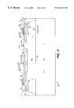
- the prior art structure ( 60 ) depicted in FIG. 1C illustrates one technique to make a connection of the source and body regions in the MOS structure to the backside ( 78 ) through the diffusion of a dopant ( 64 ) introduced from the topside ( 62 ) of the chip and a metal finger short.
- this diffusion not only moves the topside dopant ( 64 ) down and sideways but also moves the substrate dopant ( 76 ) up thus reducing the distance between the highly doped substrate interface ( 75 ) and the drain area ( 72 ) of the device.
- This diffusion movement of the interface ( 75 ) produces an increase of the minimum source-drain capacitance C ds that can be obtained under a high voltage bias V DS .
- the plug ( 82 ) connects the source and the body areas to the backside ( 95 ) through the original epitaxial layer ( 94 ) thickness without diffusion.
- the connection area ( 84 of FIG. 1D) was made small comparable to the diffusion area ( 66 of FIG. 1C) to increase the density of devices per inch 2 .
- the usage of a metal plug ( 82 of FIG. 1D) provided for a good ohmic contact in a small area ( 2 ) without long thermal processing cycles.
- the detailed prior art source-body connection structure ( 160 ) for lateral RF MOS devices is shown in FIG. 1 E.
- the structure ( 160 ) was optimized in terms of its transconductance g m and interelectrode capacitances C gs , C gd , and C ds , so that it could be used in high frequency applications, such as the cellular and the PCS regions of the RF spectrum.
- the transconductance per unit g m of the lateral RF MOS device ( 160 of FIG. 1E) was increased by fabricating the device with the smallest plug size that the technology would allow.
- the reduction in C gd capacitance of the device ( 160 of FIG. 1E) was obtained by minimizing the channel length L and by minimizing the insertion of the drain extension lateral diffusion under the gate.
- the reduction in C ds capacitance of the device ( 160 of FIG. 1E) was obtained by utilizing a high resistivity material under the drain portion of the structure ( 160 of FIG. 1E) and by separating the drain area from the source.
- a region ( 162 ) was formed in the source-body region of the semiconductor material.
- FIG. 4 depicts a detailed cross-sectional view of the lateral RF MOS transistor ( 350 ) disclosed in the patent application #1.
- the device ( 350 of FIG. 4) includes two drain drift regions ( 366 and 368 ) and a plug source-body-contact structure.
- the device structure ( 350 ) comprises: a semiconductor material comprising an epitaxial layer ( 354 ) of a first conductivity type and having an epitaxial layer dopant concentration and a top surface ( 372 ).
- the epitaxial layer's conductivity type is P-type, that is the majority carriers are holes.
- the dopant concentration of the epitaxial layer is P ⁇ , wherein ( ⁇ ) indicates that the dopant concentration P ⁇ of holes in the epitaxial layer ( 354 ) is small comparatively with the hole concentration P in the body region ( 360 ) (see discussion below).
- the typical dimensions of the epitaxial layer ( 354 ) are (3-10) ⁇ .
- the semiconductor material ( 354 ) is of a second (N) conductivity type, has a dopant concentration N ⁇ and includes a top surface ( 372 ).
- the majority carriers are holes.
- a conductive gate ( 356 ) overlies the top surface ( 372 ) of the semiconductor material.
- the gate ( 356 ) is insulated from the semiconductor material by a gate oxide layer ( 357 ).
- the gate oxide layer has the dimensions (200-700) ⁇ .
- the gate comprises a polysilicon gate.
- the region ( 366 ) forms a first enhanced drain drift region of the RF MOS structure.
- the region ( 366 ) is formed completely within the semiconductor material ( 354 ).
- the first enhanced drain drift region ( 366 ) has N conductivity type if the epitaxial layer has P conductivity type (and vice versa), and has a dopant concentration N 1 .
- the first enhanced drain region ( 366 ) has dimensions (0.1-2.5) ⁇ laterally, and about (0.2-0.5) ⁇ vertically.
- the region ( 368 ) forms a second enhanced drain drift region of the RF MOS structure that contacts the first enhanced drain drift region ( 366 ).
- the region ( 368 ) is formed completely within the semiconductor material ( 354 ).
- the second enhanced drain drift region ( 368 ) has N conductivity type if the epitaxial layer has P conductivity type (and vice versa), and has a dopant concentration N 2 that is larger than the dopant concentration N 1 of the first enhanced drain region ( 366 ):
- the second enhanced drain region ( 368 ) has dimensions (0.1-2.5) ⁇ laterally, and about (0.2-0.5) ⁇ vertically.
- the dopant concentration N 2 of the second enhanced drain region ( 366 ) is 3/2 as much as the dopant concentration N 1 of the first enhanced drain region ( 366 ):
- the structure of the lateral RF MOS device ( 350 of FIG. 4) disclosed in the patent application #1 includes two drain drift regions ( 366 and 368 ). This structure allows one to increase the maximum drain drift current density of the device and the drain-to-source breakdown voltage V breakdown of the structure ( 350 of FIG. 4) is also increased.
- the effective electrical field in the drain drift region is strong enough (about 10 kV/cm) to cause at certain critical concentration of carriers N c the avalanche effect of carrier multiplication.
- the critical carrier concentration N c is related to the breakdown voltage V breakdown , that is defined as the voltage at which the avalanche effect of carrier multiplication takes place.
- the second drain drift region ( 368 of FIG. 4) has the concentration N 2 that is higher than the concentration of the first drain drift region N 1 . This results in the redistribution of the critical electrical fields in the source-drain channel and in increase of the drain-to-source breakdown voltage V breakdown .
- the maximum current density in the source-drain channel of the device is increased because the total concentration N T :
- the drain region ( 370 ) formed in the semiconductor material ( 354 ) has the N conductivity type, if the epitaxial layer ( 354 ) has P conductivity type (and vice versa), has a dopant concentration N + that is greater than the dopant concentration N 1 of the first enhanced region ( 366 ), and greater than the dopant concentration N 2 of the second enhanced region ( 368 ).
- the drain region ( 370 ) contacts the second enhanced drain drift region ( 368 ).
- the typical dimensions of the drain region ( 370 ) are (0.5-3.0) ⁇ horizontally, and (0.1-0.3) ⁇ vertically.
- the body region ( 360 ) formed in the semiconductor material has P conductivity type if the epitaxial layer ( 354 ) has P conductivity type (and vice versa), and has a dopant concentration P ⁇ that is equal or greater than the dopant concentration P ⁇ of the epitaxial layer ( 354 ).
- the typical dimensions of the body region ( 360 ) are (0.5-1.5) ⁇ horizontally or vertically.
- the body region ( 360 ) includes a source contact region ( 362 ) being of N conductivity type N (if the epitaxial layer has P conductivity type and vice versa) and having a dopant concentration N + .
- the typical dimensions of the source contact region ( 362 ) are (0.5-1.5) ⁇ horizontally.
- the body region ( 360 ) also includes a body contact region ( 364 ) being of P conductivity type (if the epitaxial layer has P conductivity type and vice versa) and having a dopant concentration P + that is greater than the dopant concentration P ⁇ of the body region ( 360 ).
- the typical dimensions of the region ( 364 ) are (0.5-1.0) ⁇ vertically or horizontally.
- the lateral RF MOS device ( 350 of FIG. 4) also includes a conductive plug region ( 351 ) formed in the source region and the body region ( 360 ) of the semiconductor material.
- the conductive plug ( 351 of FIG. 4) can comprise a metal plug or a silicided plug.
- the silicided plug can comprise a tungsten silicided plug, a titanium silicided plug, a cobalt silicided plug, or a platinum silicided plug.
- the conductive plug region ( 204 of FIG. 2 or 351 of FIG. 4) connects a top of the source region and a lateral surface ( 209 ) of the body contact region to an interface ( 206 ) between a highly conductive substrate ( 207 ) of the RF MOS structure and an epitaxial layer ( 205 ).
- the conductive plug region ( 214 of FIG. 3) connects the top lateral surface ( 218 ) of the source region to a highly conductive substrate ( 216 ) of the RF MOS structure ( 210 ).
- FIG. 5 depicts a lateral RF MOS device ( 400 ) having a single enhanced drain drift region, a conductive plug ( 424 ), an oxide plug ( 430 ) in the drain region ( 428 ), and a body region ( 422 ).
- a conductive gate ( 414 ) overlies the top surface of the semiconductor material.
- the gate ( 414 ) is insulated from the semiconductor material by a gate oxide layer ( 416 ).
- the size of the drain area was reduced to make the drain itself smaller in order to reduce the drain-source capacitance.
- the problem with this solution was that the size of the drain electrode metal finger could become too small to support the necessary drain current density that made the device useful in its operation.
- the oxide plug ( 430 of FIG. 5) utilized in the present invention does not affect the drain current, but significantly improves (decreases) the drain-source capacitance and therefore improves the bandwidth (BW) and the power efficiency when the RF MOS device of the present invention ( 400 of FIG. 5) is used as an amplifier.
- the intrinsic capacitance inherent in the basic physical operation of the device is associated with the charges stored on the gate electrodes and the channel itself.
- the parasitic drain-source capacitance is mainly associated with the bottom physical area ( 430 ) of the drain ( 428 ) of the physical structure ( 400 ), as depicted in FIG. 5, and its value is proportional to the areas of the electrodes involved. By including an oxide plug into the drain physical area ( 430 ) one can significantly reduce the parasitic drain-source capacitance.
- the optimum area for the oxide plug ( 430 of FIG. 5) should be determined according to overall design considerations and the technology used in its fabrication.
- a reduction of parasitic capacitances improves the operation of the lateral RF MOS device because in general capacitance in a device is associated with the stored energy that has to be moved around without any benefit to the device's operation.
- the two capacitances that benefit the most from any reduction in size are the drain-gate and the drain-source capacitances.
- the drain-gate capacitance through a feedback effect increases the effective input capacitance and makes the operating limit of the device smaller.
- the drain-source capacitance appears as an additional element to match to the outside circuitry. According to Fano theorem, the efficiency of power transmission and bandwidth (BW) of the device are compromised the higher the reactive component of the impedance has to be matched. Therefore, the higher the capacitance component of the output impedance of the lateral RF MOS device the higher BW limitations for the device in the amplifier circuit.
- the drain-source capacitance also affects the ultimate efficiency of the device since the matching ability is related to the amount of power that can be extracted from the device.
- the lateral RF MOS device of the present invention 400 of FIG. 5 having the oxide plug ( 430 ) in the drain area and reduced drain-source capacitance has an improved matching ability to the outside circuitry (wider BW) and an improved power efficiency as compared to a prior art lateral RF MOS device without oxide plug in the drain area.
- the oxide plug region ( 430 of FIG. 5) comprises a shallow oxide plug region formed underneath the drain contact area.
- the shallow oxide plug region is located completely within the epitaxial layer ( 412 ).
- the drain-source capacitance is decreased by only approximately 10% if the shallow plug occupies approximately 20% of the epi layer.
- the fabrication process is a relatively easy one.
- the oxide region ( 440 of FIG. 400) comprises a deep oxide plug region formed underneath the drain contact area ( 428 ).
- the deep oxide plug region separates a top ( 411 ) or lateral surface of the drain region from a highly conductive substrate ( 410 ) of the structure ( 400 of FIG. 5 ).
- the drain-source capacitance is decreased by only approximately 15%.
- the fabrication process is a relatively difficult one.
- FIG. 6 depicts another preferred embodiment of the present invention, wherein the lateral RF MOS device structure ( 460 ) includes a conductive plug ( 468 ) in the source region, an oxide plug ( 462 ) in the drain region ( 470 ), and two enhanced drain drift regions ( 464 and 466 ).
- the device ( 460 of FIG. 6) has a shallow oxide plug region (not shown).
- the device ( 460 of FIG. 6) has a deep oxide plug region ( 462 of FIG. 6 ). (Please, see the discussion of a shallow and a deep oxide plug structure benefits above).
- the device ( 460 of FIG. 6) incorporates all benefits (reduced drain-source capacitance, improved matching ability to the outside circuitry, wider BW, and an improved power efficiency) of the device ( 400 of FIG. 5) having a conducive plug ( 424 ) in the source region ( 418 ) and an oxide plug ( 430 or 440 ) in the drain region ( 428 ), and all benefits (an increased source-drain breakdown voltage and an increased maximum drain current density) of the device disclosed in the patent application #1 that has two enhanced drain drift regions. Therefore, the lateral RF MOS device ( 460 of FIG. 6) of the present invention can be used for high power and high frequency applications.
Landscapes
- Insulated Gate Type Field-Effect Transistor (AREA)
Abstract
Description
Claims (24)
Priority Applications (1)
| Application Number | Priority Date | Filing Date | Title |
|---|---|---|---|
| US09/410,934 US6222233B1 (en) | 1999-10-04 | 1999-10-04 | Lateral RF MOS device with improved drain structure |
Applications Claiming Priority (1)
| Application Number | Priority Date | Filing Date | Title |
|---|---|---|---|
| US09/410,934 US6222233B1 (en) | 1999-10-04 | 1999-10-04 | Lateral RF MOS device with improved drain structure |
Publications (1)
| Publication Number | Publication Date |
|---|---|
| US6222233B1 true US6222233B1 (en) | 2001-04-24 |
Family
ID=23626855
Family Applications (1)
| Application Number | Title | Priority Date | Filing Date |
|---|---|---|---|
| US09/410,934 Expired - Lifetime US6222233B1 (en) | 1999-10-04 | 1999-10-04 | Lateral RF MOS device with improved drain structure |
Country Status (1)
| Country | Link |
|---|---|
| US (1) | US6222233B1 (en) |
Cited By (52)
| Publication number | Priority date | Publication date | Assignee | Title |
|---|---|---|---|---|
| US6395610B1 (en) | 1999-06-24 | 2002-05-28 | Lucent Technologies Inc. | Method of making bipolar transistor semiconductor device including graded, grown, high quality oxide layer |
| US6509230B1 (en) | 1999-06-24 | 2003-01-21 | Lucent Technologies Inc. | Non-volatile memory semiconductor device including a graded, grown, high quality oxide layer and associated methods |
| US6521496B1 (en) | 1999-06-24 | 2003-02-18 | Lucent Technologies Inc. | Non-volatile memory semiconductor device including a graded, grown, high quality control gate oxide layer and associated methods |
| US6551946B1 (en) | 1999-06-24 | 2003-04-22 | Agere Systems Inc. | Two-step oxidation process for oxidizing a silicon substrate wherein the first step is carried out at a temperature below the viscoelastic temperature of silicon dioxide and the second step is carried out at a temperature above the viscoelastic temperature |
| US20030085425A1 (en) * | 2001-11-02 | 2003-05-08 | Ultrarf, Inc. | Silicon on insulator device with improved heat removal and method of manufacture |
| US6653691B2 (en) | 2000-11-16 | 2003-11-25 | Silicon Semiconductor Corporation | Radio frequency (RF) power devices having faraday shield layers therein |
| US6670242B1 (en) | 1999-06-24 | 2003-12-30 | Agere Systems Inc. | Method for making an integrated circuit device including a graded, grown, high quality gate oxide layer and a nitride layer |
| US20040065919A1 (en) * | 2002-10-03 | 2004-04-08 | Wilson Peter H. | Trench gate laterally diffused MOSFET devices and methods for making such devices |
| US20040115790A1 (en) * | 2001-02-13 | 2004-06-17 | Tiina Pakula | Method for production of secreted proteins in fungi |
| US20040142523A1 (en) * | 2000-08-16 | 2004-07-22 | Izak Bencuya | Method of forming vertical mosfet with ultra-low on-resistance and low gate charge |
| US20040232407A1 (en) * | 1999-12-20 | 2004-11-25 | Fairchild Semiconductor Corporation | Power MOS device with improved gate charge performance |
| US20040232481A1 (en) * | 2003-05-20 | 2004-11-25 | Robert Herrick | Structure and method for forming a trench MOSFET having self-aligned features |
| US20040256690A1 (en) * | 2001-10-17 | 2004-12-23 | Kocon Christopher Boguslaw | Schottky diode using charge balance structure |
| US20050023607A1 (en) * | 2002-07-18 | 2005-02-03 | Steven Sapp | Vertical charge control semiconductor device with low output capacitance |
| US20050029618A1 (en) * | 2001-01-30 | 2005-02-10 | Marchant Bruce D. | Structure and method of forming a dual-trench field effect transistor |
| EP1515371A2 (en) | 2003-09-15 | 2005-03-16 | Infineon Technologies AG | Semiconductor device comprising a MOS transistor and method of making the same |
| US20050116313A1 (en) * | 2003-11-28 | 2005-06-02 | Lee Jae-Gil | Superjunction semiconductor device |
| US20050153497A1 (en) * | 2000-08-16 | 2005-07-14 | Izak Bencuya | Method of forming a FET having ultra-low on-resistance and low gate charge |
| US20050164516A1 (en) * | 2000-01-11 | 2005-07-28 | Agere Systems Inc. | Method and structure for graded gate oxides on vertical and non-planar surfaces |
| US20050199918A1 (en) * | 2004-03-15 | 2005-09-15 | Daniel Calafut | Optimized trench power MOSFET with integrated schottky diode |
| US20060011990A1 (en) * | 2004-07-15 | 2006-01-19 | International Business Machines Corporation | Method for fabricating strained semiconductor structures and strained semiconductor structures formed thereby |
| US6991977B2 (en) | 2001-10-17 | 2006-01-31 | Fairchild Semiconductor Corporation | Method for forming a semiconductor structure with improved smaller forward voltage loss and higher blocking capability |
| US20060076617A1 (en) * | 2004-10-08 | 2006-04-13 | Shenoy Praveen M | MOS-gated transistor with reduced miller capacitance |
| US7067876B2 (en) * | 2001-05-09 | 2006-06-27 | Kabushiki Kaisha Toshiba | Semiconductor device |
| US20060214222A1 (en) * | 2003-05-20 | 2006-09-28 | Ashok Challa | Power semiconductor devices and methods of manufacture |
| US7265416B2 (en) | 2002-02-23 | 2007-09-04 | Fairchild Korea Semiconductor Ltd. | High breakdown voltage low on-resistance lateral DMOS transistor |
| US20070246771A1 (en) * | 2002-11-22 | 2007-10-25 | Mccormack Steve | Lateral double-diffused metal oxide semiconductor (LDMOS) device with an enhanced drift region that has an improved Ron area product |
| US7319256B1 (en) | 2006-06-19 | 2008-01-15 | Fairchild Semiconductor Corporation | Shielded gate trench FET with the shield and gate electrodes being connected together |
| US7345342B2 (en) | 2001-01-30 | 2008-03-18 | Fairchild Semiconductor Corporation | Power semiconductor devices and methods of manufacture |
| US7352036B2 (en) | 2004-08-03 | 2008-04-01 | Fairchild Semiconductor Corporation | Semiconductor power device having a top-side drain using a sinker trench |
| US7368777B2 (en) | 2003-12-30 | 2008-05-06 | Fairchild Semiconductor Corporation | Accumulation device with charge balance structure and method of forming the same |
| US7385248B2 (en) | 2005-08-09 | 2008-06-10 | Fairchild Semiconductor Corporation | Shielded gate field effect transistor with improved inter-poly dielectric |
| US7446374B2 (en) | 2006-03-24 | 2008-11-04 | Fairchild Semiconductor Corporation | High density trench FET with integrated Schottky diode and method of manufacture |
| US7504306B2 (en) | 2005-04-06 | 2009-03-17 | Fairchild Semiconductor Corporation | Method of forming trench gate field effect transistor with recessed mesas |
| US20090166744A1 (en) * | 2007-12-28 | 2009-07-02 | Magnachip Semiconductor, Ltd. | Semiconductor device with deep trench structure |
| US20090194785A1 (en) * | 2008-01-11 | 2009-08-06 | Fuji Electric Device Technology Co., Ltd. | Semiconductor device and manufacturing method thereof |
| US7576388B1 (en) | 2002-10-03 | 2009-08-18 | Fairchild Semiconductor Corporation | Trench-gate LDMOS structures |
| US7582519B2 (en) | 2002-11-05 | 2009-09-01 | Fairchild Semiconductor Corporation | Method of forming a trench structure having one or more diodes embedded therein adjacent a PN junction |
| WO2009144616A1 (en) * | 2008-05-26 | 2009-12-03 | Nxp B.V. | Ldmos transistor |
| US20100117237A1 (en) * | 2008-11-12 | 2010-05-13 | Coolbaugh Douglas D | Silicided Trench Contact to Buried Conductive Layer |
| US7772668B2 (en) | 2007-12-26 | 2010-08-10 | Fairchild Semiconductor Corporation | Shielded gate trench FET with multiple channels |
| CN101719513B (en) * | 2009-11-26 | 2012-09-19 | 上海宏力半导体制造有限公司 | 30V double-diffusion MOS device and 18V double-diffusion MOS device |
| US8319290B2 (en) | 2010-06-18 | 2012-11-27 | Fairchild Semiconductor Corporation | Trench MOS barrier schottky rectifier with a planar surface using CMP techniques |
| US8673700B2 (en) | 2011-04-27 | 2014-03-18 | Fairchild Semiconductor Corporation | Superjunction structures for power devices and methods of manufacture |
| CN103871881A (en) * | 2012-12-14 | 2014-06-18 | 上海华虹宏力半导体制造有限公司 | Groove of P type LDMOS device and manufacture method of groove |
| US8772868B2 (en) | 2011-04-27 | 2014-07-08 | Fairchild Semiconductor Corporation | Superjunction structures for power devices and methods of manufacture |
| US8786010B2 (en) | 2011-04-27 | 2014-07-22 | Fairchild Semiconductor Corporation | Superjunction structures for power devices and methods of manufacture |
| US8836028B2 (en) | 2011-04-27 | 2014-09-16 | Fairchild Semiconductor Corporation | Superjunction structures for power devices and methods of manufacture |
| US8866218B2 (en) | 2011-03-29 | 2014-10-21 | Fairchild Semiconductor Corporation | Wafer level MOSFET metallization |
| US8928077B2 (en) | 2007-09-21 | 2015-01-06 | Fairchild Semiconductor Corporation | Superjunction structures for power devices |
| US20160079412A1 (en) * | 2014-09-16 | 2016-03-17 | Kabushiki Kaisha Toshiba | Semiconductor device, and method of manufacturing the same |
| US9431481B2 (en) | 2008-09-19 | 2016-08-30 | Fairchild Semiconductor Corporation | Superjunction structures for power devices and methods of manufacture |
-
1999
- 1999-10-04 US US09/410,934 patent/US6222233B1/en not_active Expired - Lifetime
Cited By (121)
| Publication number | Priority date | Publication date | Assignee | Title |
|---|---|---|---|---|
| US6509230B1 (en) | 1999-06-24 | 2003-01-21 | Lucent Technologies Inc. | Non-volatile memory semiconductor device including a graded, grown, high quality oxide layer and associated methods |
| US6521496B1 (en) | 1999-06-24 | 2003-02-18 | Lucent Technologies Inc. | Non-volatile memory semiconductor device including a graded, grown, high quality control gate oxide layer and associated methods |
| US6551946B1 (en) | 1999-06-24 | 2003-04-22 | Agere Systems Inc. | Two-step oxidation process for oxidizing a silicon substrate wherein the first step is carried out at a temperature below the viscoelastic temperature of silicon dioxide and the second step is carried out at a temperature above the viscoelastic temperature |
| US6670242B1 (en) | 1999-06-24 | 2003-12-30 | Agere Systems Inc. | Method for making an integrated circuit device including a graded, grown, high quality gate oxide layer and a nitride layer |
| US6395610B1 (en) | 1999-06-24 | 2002-05-28 | Lucent Technologies Inc. | Method of making bipolar transistor semiconductor device including graded, grown, high quality oxide layer |
| US7625793B2 (en) | 1999-12-20 | 2009-12-01 | Fairchild Semiconductor Corporation | Power MOS device with improved gate charge performance |
| US20040232407A1 (en) * | 1999-12-20 | 2004-11-25 | Fairchild Semiconductor Corporation | Power MOS device with improved gate charge performance |
| US7169714B2 (en) | 2000-01-11 | 2007-01-30 | Agere Systems, Inc. | Method and structure for graded gate oxides on vertical and non-planar surfaces |
| US20050164516A1 (en) * | 2000-01-11 | 2005-07-28 | Agere Systems Inc. | Method and structure for graded gate oxides on vertical and non-planar surfaces |
| US7745289B2 (en) | 2000-08-16 | 2010-06-29 | Fairchild Semiconductor Corporation | Method of forming a FET having ultra-low on-resistance and low gate charge |
| US20050153497A1 (en) * | 2000-08-16 | 2005-07-14 | Izak Bencuya | Method of forming a FET having ultra-low on-resistance and low gate charge |
| US20040142523A1 (en) * | 2000-08-16 | 2004-07-22 | Izak Bencuya | Method of forming vertical mosfet with ultra-low on-resistance and low gate charge |
| US20100258864A1 (en) * | 2000-08-16 | 2010-10-14 | Izak Bencuya | Method of Forming a FET Having Ultra-low On-resistance and Low Gate Charge |
| US8101484B2 (en) | 2000-08-16 | 2012-01-24 | Fairchild Semiconductor Corporation | Method of forming a FET having ultra-low on-resistance and low gate charge |
| US8710584B2 (en) | 2000-08-16 | 2014-04-29 | Fairchild Semiconductor Corporation | FET device having ultra-low on-resistance and low gate charge |
| US6653691B2 (en) | 2000-11-16 | 2003-11-25 | Silicon Semiconductor Corporation | Radio frequency (RF) power devices having faraday shield layers therein |
| US9368587B2 (en) | 2001-01-30 | 2016-06-14 | Fairchild Semiconductor Corporation | Accumulation-mode field effect transistor with improved current capability |
| US20110014764A1 (en) * | 2001-01-30 | 2011-01-20 | Marchant Bruce D | Method of forming a dual-trench field effect transistor |
| US20050029618A1 (en) * | 2001-01-30 | 2005-02-10 | Marchant Bruce D. | Structure and method of forming a dual-trench field effect transistor |
| US8829641B2 (en) | 2001-01-30 | 2014-09-09 | Fairchild Semiconductor Corporation | Method of forming a dual-trench field effect transistor |
| US7345342B2 (en) | 2001-01-30 | 2008-03-18 | Fairchild Semiconductor Corporation | Power semiconductor devices and methods of manufacture |
| US20040115790A1 (en) * | 2001-02-13 | 2004-06-17 | Tiina Pakula | Method for production of secreted proteins in fungi |
| US7067876B2 (en) * | 2001-05-09 | 2006-06-27 | Kabushiki Kaisha Toshiba | Semiconductor device |
| US7061066B2 (en) | 2001-10-17 | 2006-06-13 | Fairchild Semiconductor Corporation | Schottky diode using charge balance structure |
| US6991977B2 (en) | 2001-10-17 | 2006-01-31 | Fairchild Semiconductor Corporation | Method for forming a semiconductor structure with improved smaller forward voltage loss and higher blocking capability |
| US20040256690A1 (en) * | 2001-10-17 | 2004-12-23 | Kocon Christopher Boguslaw | Schottky diode using charge balance structure |
| US7429523B2 (en) | 2001-10-17 | 2008-09-30 | Fairchild Semiconductor Corporation | Method of forming schottky diode with charge balance structure |
| US20030085425A1 (en) * | 2001-11-02 | 2003-05-08 | Ultrarf, Inc. | Silicon on insulator device with improved heat removal and method of manufacture |
| US6900501B2 (en) | 2001-11-02 | 2005-05-31 | Cree Microwave, Inc. | Silicon on insulator device with improved heat removal |
| US6740548B2 (en) | 2001-11-02 | 2004-05-25 | Cree Microwave, Inc. | Method of manufacture of silicon on insulator device with improved heat removal |
| US20030107084A1 (en) * | 2001-11-02 | 2003-06-12 | Cree Microwave, Inc. | Method of manufacture of silicon on insulator device with improved heat removal |
| US7265416B2 (en) | 2002-02-23 | 2007-09-04 | Fairchild Korea Semiconductor Ltd. | High breakdown voltage low on-resistance lateral DMOS transistor |
| US7605040B2 (en) | 2002-02-23 | 2009-10-20 | Fairchild Korea Semiconductor Ltd. | Method of forming high breakdown voltage low on-resistance lateral DMOS transistor |
| US7977744B2 (en) | 2002-07-18 | 2011-07-12 | Fairchild Semiconductor Corporation | Field effect transistor with trench filled with insulating material and strips of semi-insulating material along trench sidewalls |
| US20050023607A1 (en) * | 2002-07-18 | 2005-02-03 | Steven Sapp | Vertical charge control semiconductor device with low output capacitance |
| US7291894B2 (en) | 2002-07-18 | 2007-11-06 | Fairchild Semiconductor Corporation | Vertical charge control semiconductor device with low output capacitance |
| US7033891B2 (en) | 2002-10-03 | 2006-04-25 | Fairchild Semiconductor Corporation | Trench gate laterally diffused MOSFET devices and methods for making such devices |
| US20040065919A1 (en) * | 2002-10-03 | 2004-04-08 | Wilson Peter H. | Trench gate laterally diffused MOSFET devices and methods for making such devices |
| US8198677B2 (en) | 2002-10-03 | 2012-06-12 | Fairchild Semiconductor Corporation | Trench-gate LDMOS structures |
| US7576388B1 (en) | 2002-10-03 | 2009-08-18 | Fairchild Semiconductor Corporation | Trench-gate LDMOS structures |
| US7582519B2 (en) | 2002-11-05 | 2009-09-01 | Fairchild Semiconductor Corporation | Method of forming a trench structure having one or more diodes embedded therein adjacent a PN junction |
| US7635621B2 (en) | 2002-11-22 | 2009-12-22 | Micrel, Inc. | Lateral double-diffused metal oxide semiconductor (LDMOS) device with an enhanced drift region that has an improved Ron area product |
| US20070246771A1 (en) * | 2002-11-22 | 2007-10-25 | Mccormack Steve | Lateral double-diffused metal oxide semiconductor (LDMOS) device with an enhanced drift region that has an improved Ron area product |
| US7638841B2 (en) | 2003-05-20 | 2009-12-29 | Fairchild Semiconductor Corporation | Power semiconductor devices and methods of manufacture |
| US8013391B2 (en) | 2003-05-20 | 2011-09-06 | Fairchild Semiconductor Corporation | Power semiconductor devices with trenched shielded split gate transistor and methods of manufacture |
| US20040232481A1 (en) * | 2003-05-20 | 2004-11-25 | Robert Herrick | Structure and method for forming a trench MOSFET having self-aligned features |
| US8936985B2 (en) | 2003-05-20 | 2015-01-20 | Fairchild Semiconductor Corporation | Methods related to power semiconductor devices with thick bottom oxide layers |
| US8889511B2 (en) | 2003-05-20 | 2014-11-18 | Fairchild Semiconductor Corporation | Methods of manufacturing power semiconductor devices with trenched shielded split gate transistor |
| US8786045B2 (en) | 2003-05-20 | 2014-07-22 | Fairchild Semiconductor Corporation | Power semiconductor devices having termination structures |
| US8716783B2 (en) | 2003-05-20 | 2014-05-06 | Fairchild Semiconductor Corporation | Power device with self-aligned source regions |
| US8350317B2 (en) | 2003-05-20 | 2013-01-08 | Fairchild Semiconductor Corporation | Power semiconductor devices and methods of manufacture |
| US6916745B2 (en) | 2003-05-20 | 2005-07-12 | Fairchild Semiconductor Corporation | Structure and method for forming a trench MOSFET having self-aligned features |
| US8143123B2 (en) | 2003-05-20 | 2012-03-27 | Fairchild Semiconductor Corporation | Methods of forming inter-poly dielectric (IPD) layers in power semiconductor devices |
| US8143124B2 (en) | 2003-05-20 | 2012-03-27 | Fairchild Semiconductor Corporation | Methods of making power semiconductor devices with thick bottom oxide layer |
| US8129245B2 (en) | 2003-05-20 | 2012-03-06 | Fairchild Semiconductor Corporation | Methods of manufacturing power semiconductor devices with shield and gate contacts |
| US7595524B2 (en) | 2003-05-20 | 2009-09-29 | Fairchild Semiconductor Corporation | Power device with trenches having wider upper portion than lower portion |
| US8034682B2 (en) | 2003-05-20 | 2011-10-11 | Fairchild Semiconductor Corporation | Power device with trenches having wider upper portion than lower portion |
| US7344943B2 (en) | 2003-05-20 | 2008-03-18 | Fairchild Semiconductor Corporation | Method for forming a trench MOSFET having self-aligned features |
| US8013387B2 (en) | 2003-05-20 | 2011-09-06 | Fairchild Semiconductor Corporation | Power semiconductor devices with shield and gate contacts and methods of manufacture |
| US7982265B2 (en) | 2003-05-20 | 2011-07-19 | Fairchild Semiconductor Corporation | Trenched shield gate power semiconductor devices and methods of manufacture |
| US20110003449A1 (en) * | 2003-05-20 | 2011-01-06 | Robert Herrick | Power Device With Trenches Having Wider Upper Portion Than Lower Portion |
| US7855415B2 (en) | 2003-05-20 | 2010-12-21 | Fairchild Semiconductor Corporation | Power semiconductor devices having termination structures and methods of manufacture |
| US20100015769A1 (en) * | 2003-05-20 | 2010-01-21 | Robert Herrick | Power Device With Trenches Having Wider Upper Portion Than Lower Portion |
| US7652326B2 (en) | 2003-05-20 | 2010-01-26 | Fairchild Semiconductor Corporation | Power semiconductor devices and methods of manufacture |
| US7799636B2 (en) | 2003-05-20 | 2010-09-21 | Fairchild Semiconductor Corporation | Power device with trenches having wider upper portion than lower portion |
| US20060214222A1 (en) * | 2003-05-20 | 2006-09-28 | Ashok Challa | Power semiconductor devices and methods of manufacture |
| EP1515371A2 (en) | 2003-09-15 | 2005-03-16 | Infineon Technologies AG | Semiconductor device comprising a MOS transistor and method of making the same |
| EP1515371A3 (en) * | 2003-09-15 | 2008-03-26 | Infineon Technologies AG | Semiconductor device comprising a MOS transistor and method of making the same |
| US7301203B2 (en) | 2003-11-28 | 2007-11-27 | Fairchild Korea Semiconductor Ltd. | Superjunction semiconductor device |
| US20050116313A1 (en) * | 2003-11-28 | 2005-06-02 | Lee Jae-Gil | Superjunction semiconductor device |
| US7655981B2 (en) | 2003-11-28 | 2010-02-02 | Fairchild Korea Semiconductor Ltd. | Superjunction semiconductor device |
| US20080211053A1 (en) * | 2003-11-28 | 2008-09-04 | Fairchild Korea Semiconductor Ltd. | Superjunction Semiconductor Device |
| US7368777B2 (en) | 2003-12-30 | 2008-05-06 | Fairchild Semiconductor Corporation | Accumulation device with charge balance structure and method of forming the same |
| US7936008B2 (en) | 2003-12-30 | 2011-05-03 | Fairchild Semiconductor Corporation | Structure and method for forming accumulation-mode field effect transistor with improved current capability |
| US8518777B2 (en) | 2003-12-30 | 2013-08-27 | Fairchild Semiconductor Corporation | Method for forming accumulation-mode field effect transistor with improved current capability |
| US20050199918A1 (en) * | 2004-03-15 | 2005-09-15 | Daniel Calafut | Optimized trench power MOSFET with integrated schottky diode |
| US7102201B2 (en) * | 2004-07-15 | 2006-09-05 | International Business Machines Corporation | Strained semiconductor device structures |
| US20060011990A1 (en) * | 2004-07-15 | 2006-01-19 | International Business Machines Corporation | Method for fabricating strained semiconductor structures and strained semiconductor structures formed thereby |
| US7352036B2 (en) | 2004-08-03 | 2008-04-01 | Fairchild Semiconductor Corporation | Semiconductor power device having a top-side drain using a sinker trench |
| US8148233B2 (en) | 2004-08-03 | 2012-04-03 | Fairchild Semiconductor Corporation | Semiconductor power device having a top-side drain using a sinker trench |
| US7732876B2 (en) | 2004-08-03 | 2010-06-08 | Fairchild Semiconductor Corporation | Power transistor with trench sinker for contacting the backside |
| US8026558B2 (en) | 2004-08-03 | 2011-09-27 | Fairchild Semiconductor Corporation | Semiconductor power device having a top-side drain using a sinker trench |
| US7265415B2 (en) | 2004-10-08 | 2007-09-04 | Fairchild Semiconductor Corporation | MOS-gated transistor with reduced miller capacitance |
| US20060076617A1 (en) * | 2004-10-08 | 2006-04-13 | Shenoy Praveen M | MOS-gated transistor with reduced miller capacitance |
| US7534683B2 (en) | 2004-10-08 | 2009-05-19 | Fairchild Semiconductor Corporation | Method of making a MOS-gated transistor with reduced miller capacitance |
| US8680611B2 (en) | 2005-04-06 | 2014-03-25 | Fairchild Semiconductor Corporation | Field effect transistor and schottky diode structures |
| US8084327B2 (en) | 2005-04-06 | 2011-12-27 | Fairchild Semiconductor Corporation | Method for forming trench gate field effect transistor with recessed mesas using spacers |
| US7504306B2 (en) | 2005-04-06 | 2009-03-17 | Fairchild Semiconductor Corporation | Method of forming trench gate field effect transistor with recessed mesas |
| US7598144B2 (en) | 2005-08-09 | 2009-10-06 | Fairchild Semiconductor Corporation | Method for forming inter-poly dielectric in shielded gate field effect transistor |
| US7385248B2 (en) | 2005-08-09 | 2008-06-10 | Fairchild Semiconductor Corporation | Shielded gate field effect transistor with improved inter-poly dielectric |
| US7446374B2 (en) | 2006-03-24 | 2008-11-04 | Fairchild Semiconductor Corporation | High density trench FET with integrated Schottky diode and method of manufacture |
| US7713822B2 (en) | 2006-03-24 | 2010-05-11 | Fairchild Semiconductor Corporation | Method of forming high density trench FET with integrated Schottky diode |
| US7859047B2 (en) | 2006-06-19 | 2010-12-28 | Fairchild Semiconductor Corporation | Shielded gate trench FET with the shield and gate electrodes connected together in non-active region |
| US7473603B2 (en) | 2006-06-19 | 2009-01-06 | Fairchild Semiconductor Corporation | Method for forming a shielded gate trench FET with the shield and gate electrodes being connected together |
| US7319256B1 (en) | 2006-06-19 | 2008-01-15 | Fairchild Semiconductor Corporation | Shielded gate trench FET with the shield and gate electrodes being connected together |
| US9595596B2 (en) | 2007-09-21 | 2017-03-14 | Fairchild Semiconductor Corporation | Superjunction structures for power devices |
| US8928077B2 (en) | 2007-09-21 | 2015-01-06 | Fairchild Semiconductor Corporation | Superjunction structures for power devices |
| US20100258866A1 (en) * | 2007-12-26 | 2010-10-14 | James Pan | Method for Forming Shielded Gate Trench FET with Multiple Channels |
| US9224853B2 (en) | 2007-12-26 | 2015-12-29 | Fairchild Semiconductor Corporation | Shielded gate trench FET with multiple channels |
| US7772668B2 (en) | 2007-12-26 | 2010-08-10 | Fairchild Semiconductor Corporation | Shielded gate trench FET with multiple channels |
| US20090166744A1 (en) * | 2007-12-28 | 2009-07-02 | Magnachip Semiconductor, Ltd. | Semiconductor device with deep trench structure |
| US8049283B2 (en) * | 2007-12-28 | 2011-11-01 | Magnachip Semiconductor, Ltd. | Semiconductor device with deep trench structure |
| US7999317B2 (en) * | 2008-01-11 | 2011-08-16 | Fuji Electric Systems Co., Ltd. | Semiconductor device and manufacturing method thereof |
| US20090194785A1 (en) * | 2008-01-11 | 2009-08-06 | Fuji Electric Device Technology Co., Ltd. | Semiconductor device and manufacturing method thereof |
| WO2009144616A1 (en) * | 2008-05-26 | 2009-12-03 | Nxp B.V. | Ldmos transistor |
| US9431481B2 (en) | 2008-09-19 | 2016-08-30 | Fairchild Semiconductor Corporation | Superjunction structures for power devices and methods of manufacture |
| US8872281B2 (en) | 2008-11-12 | 2014-10-28 | International Business Machines Corporation | Silicided trench contact to buried conductive layer |
| US20100117237A1 (en) * | 2008-11-12 | 2010-05-13 | Coolbaugh Douglas D | Silicided Trench Contact to Buried Conductive Layer |
| US8338265B2 (en) | 2008-11-12 | 2012-12-25 | International Business Machines Corporation | Silicided trench contact to buried conductive layer |
| CN101719513B (en) * | 2009-11-26 | 2012-09-19 | 上海宏力半导体制造有限公司 | 30V double-diffusion MOS device and 18V double-diffusion MOS device |
| US8432000B2 (en) | 2010-06-18 | 2013-04-30 | Fairchild Semiconductor Corporation | Trench MOS barrier schottky rectifier with a planar surface using CMP techniques |
| US8319290B2 (en) | 2010-06-18 | 2012-11-27 | Fairchild Semiconductor Corporation | Trench MOS barrier schottky rectifier with a planar surface using CMP techniques |
| US8866218B2 (en) | 2011-03-29 | 2014-10-21 | Fairchild Semiconductor Corporation | Wafer level MOSFET metallization |
| US8836028B2 (en) | 2011-04-27 | 2014-09-16 | Fairchild Semiconductor Corporation | Superjunction structures for power devices and methods of manufacture |
| US8673700B2 (en) | 2011-04-27 | 2014-03-18 | Fairchild Semiconductor Corporation | Superjunction structures for power devices and methods of manufacture |
| US8786010B2 (en) | 2011-04-27 | 2014-07-22 | Fairchild Semiconductor Corporation | Superjunction structures for power devices and methods of manufacture |
| US8772868B2 (en) | 2011-04-27 | 2014-07-08 | Fairchild Semiconductor Corporation | Superjunction structures for power devices and methods of manufacture |
| CN103871881A (en) * | 2012-12-14 | 2014-06-18 | 上海华虹宏力半导体制造有限公司 | Groove of P type LDMOS device and manufacture method of groove |
| CN103871881B (en) * | 2012-12-14 | 2017-04-05 | 上海华虹宏力半导体制造有限公司 | The groove and preparation method of p-type LDMOS device |
| US20160079412A1 (en) * | 2014-09-16 | 2016-03-17 | Kabushiki Kaisha Toshiba | Semiconductor device, and method of manufacturing the same |
| US9530881B2 (en) * | 2014-09-16 | 2016-12-27 | Kabushiki Kaisha Toshiba | Semiconductor device, and method of manufacturing the same |
Similar Documents
| Publication | Publication Date | Title |
|---|---|---|
| US6222233B1 (en) | Lateral RF MOS device with improved drain structure | |
| US6271552B1 (en) | Lateral RF MOS device with improved breakdown voltage | |
| US5949104A (en) | Source connection structure for lateral RF MOS devices | |
| US7888735B2 (en) | Integrated complementary low voltage RF-LDMOS | |
| US6831332B2 (en) | Microwave field effect transistor structure | |
| US5146298A (en) | Device which functions as a lateral double-diffused insulated gate field effect transistor or as a bipolar transistor | |
| US6064088A (en) | RF power MOSFET device with extended linear region of transconductance characteristic at low drain current | |
| JP2004501501A (en) | Decoupling capacitors for thin gate oxides | |
| US6686627B2 (en) | Multiple conductive plug structure for lateral RF MOS devices | |
| KR20010101010A (en) | Offset drain fermi-threshold field effect transistors | |
| EP1058949B1 (en) | Rf mos transistor | |
| US20070096146A1 (en) | III-V power field effect transistors | |
| US6734509B2 (en) | Semiconductor integrated circuit | |
| US6838731B1 (en) | Microwave transistor structure having step drain region | |
| US20020017682A1 (en) | Semiconductor device | |
| US6762456B1 (en) | Multiple conductive plug structure including at least one conductive plug region and at least one between-conductive-plug region for lateral RF MOS devices | |
| JP3402043B2 (en) | Field effect transistor | |
| CN100546032C (en) | Semiconductor device including field effect transistor and method of operating the same | |
| JPS5846874B2 (en) | Junction field effect transistor | |
| KR102636054B1 (en) | Active Inductor Device Consisting of Single MOSFET | |
| JP3462255B2 (en) | Field effect transistor | |
| JP2004063922A (en) | Semiconductor device |
Legal Events
| Date | Code | Title | Description |
|---|---|---|---|
| AS | Assignment |
Owner name: XEMOD, INC., CALIFORNIA Free format text: ASSIGNMENT OF ASSIGNORS INTEREST;ASSIGNOR:D'ANNA, PABLO EUGENIO;REEL/FRAME:010302/0062 Effective date: 19991001 |
|
| STCF | Information on status: patent grant |
Free format text: PATENTED CASE |
|
| AS | Assignment |
Owner name: SILICON VALLEY BANK, CALIFORNIA Free format text: SECURITY INTEREST;ASSIGNOR:XEMOD, INC.;REEL/FRAME:012232/0508 Effective date: 20000222 |
|
| AS | Assignment |
Owner name: XEMOD, INC., ARIZONA Free format text: RELEASE;ASSIGNOR:SILICON VALLEY BANK;REEL/FRAME:012376/0613 Effective date: 20020204 |
|
| AS | Assignment |
Owner name: SIRENZA MICRODEVICES, INC., COLORADO Free format text: ASSIGNMENT OF ASSIGNORS INTEREST;ASSIGNOR:XEMOD, INC.;REEL/FRAME:014462/0325 Effective date: 20030808 |
|
| REMI | Maintenance fee reminder mailed | ||
| FPAY | Fee payment |
Year of fee payment: 4 |
|
| SULP | Surcharge for late payment | ||
| AS | Assignment |
Owner name: RF MICRO DEVICES, INC., NORTH CAROLINA Free format text: ASSIGNMENT OF ASSIGNORS INTEREST;ASSIGNOR:SIRENZA MICRODEVICES;REEL/FRAME:020927/0907 Effective date: 20080505 |
|
| FPAY | Fee payment |
Year of fee payment: 8 |
|
| FPAY | Fee payment |
Year of fee payment: 12 |
|
| AS | Assignment |
Owner name: BANK OF AMERICA, N.A., AS ADMINISTRATIVE AGENT, TE Free format text: NOTICE OF GRANT OF SECURITY INTEREST IN PATENTS;ASSIGNOR:RF MICRO DEVICES, INC.;REEL/FRAME:030045/0831 Effective date: 20130319 |
|
| AS | Assignment |
Owner name: RF MICRO DEVICES, INC., NORTH CAROLINA Free format text: CORRECTIVE ASSIGNMENT TO CORRECT THE NAME OF THE ASSIGNOR TO SIRENZA MICRODEVICES, INC. PREVIOUSLY RECORDED ON REEL 020927 FRAME 0907. ASSIGNOR(S) HEREBY CONFIRMS THE NAME OF THE ASSIGNEE IS RF MICRO DEVICES, INC.;ASSIGNOR:SIRENZA MICRODEVICES, INC.;REEL/FRAME:030194/0769 Effective date: 20080505 |
|
| AS | Assignment |
Owner name: RF MICRO DEVICES, INC., NORTH CAROLINA Free format text: TERMINATION AND RELEASE OF SECURITY INTEREST IN PATENTS (RECORDED 3/19/13 AT REEL/FRAME 030045/0831);ASSIGNOR:BANK OF AMERICA, N.A., AS ADMINISTRATIVE AGENT;REEL/FRAME:035334/0363 Effective date: 20150326 |
|
| AS | Assignment |
Owner name: QORVO US, INC., NORTH CAROLINA Free format text: MERGER;ASSIGNOR:RF MICRO DEVICES, INC.;REEL/FRAME:039196/0941 Effective date: 20160330 |