US6211530B1 - Sparse-carrier devices and method of fabrication - Google Patents
Sparse-carrier devices and method of fabrication Download PDFInfo
- Publication number
- US6211530B1 US6211530B1 US09/097,026 US9702698A US6211530B1 US 6211530 B1 US6211530 B1 US 6211530B1 US 9702698 A US9702698 A US 9702698A US 6211530 B1 US6211530 B1 US 6211530B1
- Authority
- US
- United States
- Prior art keywords
- quantum dots
- row
- adjacent
- rows
- distance
- Prior art date
- Legal status (The legal status is an assumption and is not a legal conclusion. Google has not performed a legal analysis and makes no representation as to the accuracy of the status listed.)
- Expired - Lifetime
Links
Images


Classifications
-
- H—ELECTRICITY
- H10—SEMICONDUCTOR DEVICES; ELECTRIC SOLID-STATE DEVICES NOT OTHERWISE PROVIDED FOR
- H10P—GENERIC PROCESSES OR APPARATUS FOR THE MANUFACTURE OR TREATMENT OF DEVICES COVERED BY CLASS H10
- H10P14/00—Formation of materials, e.g. in the shape of layers or pillars
- H10P14/20—Formation of materials, e.g. in the shape of layers or pillars of semiconductor materials
- H10P14/29—Formation of materials, e.g. in the shape of layers or pillars of semiconductor materials characterised by the substrates
- H10P14/2901—Materials
- H10P14/2907—Materials being Group IIIA-VA materials
- H10P14/2911—Arsenides
-
- B—PERFORMING OPERATIONS; TRANSPORTING
- B82—NANOTECHNOLOGY
- B82Y—SPECIFIC USES OR APPLICATIONS OF NANOSTRUCTURES; MEASUREMENT OR ANALYSIS OF NANOSTRUCTURES; MANUFACTURE OR TREATMENT OF NANOSTRUCTURES
- B82Y10/00—Nanotechnology for information processing, storage or transmission, e.g. quantum computing or single electron logic
-
- H—ELECTRICITY
- H10—SEMICONDUCTOR DEVICES; ELECTRIC SOLID-STATE DEVICES NOT OTHERWISE PROVIDED FOR
- H10D—INORGANIC ELECTRIC SEMICONDUCTOR DEVICES
- H10D30/00—Field-effect transistors [FET]
- H10D30/40—FETs having zero-dimensional [0D], one-dimensional [1D] or two-dimensional [2D] charge carrier gas channels
- H10D30/402—Single electron transistors; Coulomb blockade transistors
-
- H—ELECTRICITY
- H10—SEMICONDUCTOR DEVICES; ELECTRIC SOLID-STATE DEVICES NOT OTHERWISE PROVIDED FOR
- H10D—INORGANIC ELECTRIC SEMICONDUCTOR DEVICES
- H10D62/00—Semiconductor bodies, or regions thereof, of devices having potential barriers
- H10D62/40—Crystalline structures
- H10D62/405—Orientations of crystalline planes
-
- H—ELECTRICITY
- H10—SEMICONDUCTOR DEVICES; ELECTRIC SOLID-STATE DEVICES NOT OTHERWISE PROVIDED FOR
- H10D—INORGANIC ELECTRIC SEMICONDUCTOR DEVICES
- H10D62/00—Semiconductor bodies, or regions thereof, of devices having potential barriers
- H10D62/80—Semiconductor bodies, or regions thereof, of devices having potential barriers characterised by the materials
- H10D62/81—Semiconductor bodies, or regions thereof, of devices having potential barriers characterised by the materials of structures exhibiting quantum-confinement effects, e.g. single quantum wells; of structures having periodic or quasi-periodic potential variation
- H10D62/812—Single quantum well structures
- H10D62/814—Quantum box structures
-
- H—ELECTRICITY
- H10—SEMICONDUCTOR DEVICES; ELECTRIC SOLID-STATE DEVICES NOT OTHERWISE PROVIDED FOR
- H10P—GENERIC PROCESSES OR APPARATUS FOR THE MANUFACTURE OR TREATMENT OF DEVICES COVERED BY CLASS H10
- H10P14/00—Formation of materials, e.g. in the shape of layers or pillars
- H10P14/20—Formation of materials, e.g. in the shape of layers or pillars of semiconductor materials
- H10P14/24—Formation of materials, e.g. in the shape of layers or pillars of semiconductor materials using chemical vapour deposition [CVD]
-
- H—ELECTRICITY
- H10—SEMICONDUCTOR DEVICES; ELECTRIC SOLID-STATE DEVICES NOT OTHERWISE PROVIDED FOR
- H10P—GENERIC PROCESSES OR APPARATUS FOR THE MANUFACTURE OR TREATMENT OF DEVICES COVERED BY CLASS H10
- H10P14/00—Formation of materials, e.g. in the shape of layers or pillars
- H10P14/20—Formation of materials, e.g. in the shape of layers or pillars of semiconductor materials
- H10P14/27—Formation of materials, e.g. in the shape of layers or pillars of semiconductor materials using selective deposition, e.g. simultaneous growth of monocrystalline and non-monocrystalline semiconductor materials
- H10P14/271—Formation of materials, e.g. in the shape of layers or pillars of semiconductor materials using selective deposition, e.g. simultaneous growth of monocrystalline and non-monocrystalline semiconductor materials characterised by the preparation of substrate for selective deposition
- H10P14/272—Formation of materials, e.g. in the shape of layers or pillars of semiconductor materials using selective deposition, e.g. simultaneous growth of monocrystalline and non-monocrystalline semiconductor materials characterised by the preparation of substrate for selective deposition using mask materials other than SiO2 or SiN
-
- H—ELECTRICITY
- H10—SEMICONDUCTOR DEVICES; ELECTRIC SOLID-STATE DEVICES NOT OTHERWISE PROVIDED FOR
- H10P—GENERIC PROCESSES OR APPARATUS FOR THE MANUFACTURE OR TREATMENT OF DEVICES COVERED BY CLASS H10
- H10P14/00—Formation of materials, e.g. in the shape of layers or pillars
- H10P14/20—Formation of materials, e.g. in the shape of layers or pillars of semiconductor materials
- H10P14/32—Formation of materials, e.g. in the shape of layers or pillars of semiconductor materials characterised by intermediate layers between substrates and deposited layers
- H10P14/3202—Materials thereof
- H10P14/3214—Materials thereof being Group IIIA-VA semiconductors
- H10P14/3221—Arsenides
-
- H—ELECTRICITY
- H10—SEMICONDUCTOR DEVICES; ELECTRIC SOLID-STATE DEVICES NOT OTHERWISE PROVIDED FOR
- H10P—GENERIC PROCESSES OR APPARATUS FOR THE MANUFACTURE OR TREATMENT OF DEVICES COVERED BY CLASS H10
- H10P14/00—Formation of materials, e.g. in the shape of layers or pillars
- H10P14/20—Formation of materials, e.g. in the shape of layers or pillars of semiconductor materials
- H10P14/32—Formation of materials, e.g. in the shape of layers or pillars of semiconductor materials characterised by intermediate layers between substrates and deposited layers
- H10P14/3242—Structure
-
- H—ELECTRICITY
- H10—SEMICONDUCTOR DEVICES; ELECTRIC SOLID-STATE DEVICES NOT OTHERWISE PROVIDED FOR
- H10P—GENERIC PROCESSES OR APPARATUS FOR THE MANUFACTURE OR TREATMENT OF DEVICES COVERED BY CLASS H10
- H10P14/00—Formation of materials, e.g. in the shape of layers or pillars
- H10P14/20—Formation of materials, e.g. in the shape of layers or pillars of semiconductor materials
- H10P14/34—Deposited materials, e.g. layers
- H10P14/3402—Deposited materials, e.g. layers characterised by the chemical composition
- H10P14/3414—Deposited materials, e.g. layers characterised by the chemical composition being group IIIA-VIA materials
- H10P14/3421—Arsenides
-
- H—ELECTRICITY
- H10—SEMICONDUCTOR DEVICES; ELECTRIC SOLID-STATE DEVICES NOT OTHERWISE PROVIDED FOR
- H10P—GENERIC PROCESSES OR APPARATUS FOR THE MANUFACTURE OR TREATMENT OF DEVICES COVERED BY CLASS H10
- H10P14/00—Formation of materials, e.g. in the shape of layers or pillars
- H10P14/20—Formation of materials, e.g. in the shape of layers or pillars of semiconductor materials
- H10P14/34—Deposited materials, e.g. layers
- H10P14/3451—Structure
- H10P14/3452—Microstructure
- H10P14/3461—Nanoparticles
Definitions
- the present invention pertains to devices that operate through the conduction of a very small number of electrical carriers and to methods of fabricating the devices.
- a 3-D confined nanostructure is a small particle of material, e.g., semiconductor material, that is small enough to be quantum confined in three dimensions. That is, the quantum contained particle has a diameter that is only about 200 ⁇ or less. This creates a three dimensional well with quantum confinement in all directions.
- a sparse-carrier device including a crystal structure formed of a first material and having a crystallographic facet with contact structures at opposite ends of the length.
- Quantum dots are formed of a second material, using self-aligned techniques, and positioned in a plurality of rows on the crystallographic facet with each row extending along the length of the crystallographic facet and being approximately one quantum dot wide and a plurality of quantum dots long.
- the crystallographic facet is defined with a width to restrict formation of the second material thereon to the plurality of quantum dot wide rows of quantum dots.
- the quantum dots in a first row of the plurality of rows are separated from adjacent quantum dots in the first row by a first distance smaller than a second distance between the quantum dots in the first row and adjacent quantum dots in an adjacent row, and the quantum dots in the second row are separated from adjacent quantum dots in the second row by the first distance smaller than the second distance between the quantum dots in the second row and adjacent quantum dots in the first row.
- the first distance is small enough to allow carrier tunneling between adjacent quantum dots along a row and the second distance is large enough to substantially prevent tunneling between adjacent quantum dots between rows while being small enough to allow Coulombic interaction between adjacent quantum dots between rows.
- Electrical contacts are positioned on the contact structures at opposite ends of the rows with the electrical contacts being spaced from the quantum dots in the plurality of rows a distance to allow tunneling of carriers into and out of quantum dots in the plurality of rows.
- a first row of the plurality of rows of quantum dots is connected to receive input signals and a second parallel spaced apart row of the plurality of rows of quantum dots is connected to provide an output signal.
- the quantum dots in the second row are charged oppositely to quantum dots in the first row by Coulombic interaction between adjacent quantum dots so that output signals from the second row are inverted from input signals supplied to the first row.
- a method is disclosed of fabricating a sparse-carrier device including the steps of providing a crystal substrate of a first material and forming a crystal structure on the crystal substrate, the crystal structure being formed by growing a crystallographic facet of the first material with a predetermined width and length.
- Quantum dots of a second material are then selectively grown, using self-aligned techniques, in a plurality of rows on the crystallographic facet with each of the rows extending in parallel spaced apart relationship along the length of the crystallographic facet and being approximately one quantum dot wide and a plurality of quantum dots long.
- the plurality of rows of quantum dots are further selectively grown so that the quantum dots in a first row of the plurality of rows are separated from adjacent quantum dots in the first row by a first distance smaller than a second distance between the quantum dots in the first row and adjacent quantum dots in an adjacent second row, and the quantum dots in the second row are separated from adjacent quantum dots in the second row by the first distance smaller than the second distance between the quantum dots in the second row and adjacent quantum dots in the first row.
- the first distance is small enough to allow carrier tunneling between adjacent quantum dots within each of the rows and the second distance is large enough to substantially prevent tunneling between adjacent quantum dots between rows and small enough to allow Coulombic interaction between adjacent quantum dots between rows.
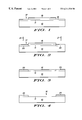
- FIGS. 1 through 4 are greatly enlarged, simplified sectional views illustrating a preferred method of patterning a substrate for further processing
- FIG. 5 is a greatly enlarged, simplified sectional view illustrating crystalline material with a facet selectively grown on the patterned substrate of FIG. 4 in accordance with the present invention
- FIG. 6 is a greatly enlarged, simplified sectional view illustrating a plurality of rows of quantum dots selectively grown on the facet of the crystalline material illustrated in FIG. 5 in accordance with the present invention
- FIG. 7 is an enlarged view in top plan of a sparse-carrier device in accordance with the present invention.
- FIG. 8 is a greatly enlarged sectional view as seen generally from the line 8 — 8 in FIG. 7;
- FIG. 9 illustrates typical input and output waveforms for the sparse-carrier device of FIG. 7 .
- FIGS. 1-4 illustrate several steps in a preferred method of masking a gallium arsenide substrate 10 for the fabrication of sparse carrier devices. While the present masking method is utilized because of its convenience (the substrate does not have to be removed from the growth chamber throughout the operation), other masking methods known in the semiconductor art may be utilized, if desired. It should be understood that gallium arsenide substrate 10 is utilized herein for purposes of this description but other III-V compounds and other semiconductor materials may be utilized in other applications. Referring specifically to FIG. 1, a simplified sectional view of gallium arsenide substrate 10 having a surface 11 is illustrated. It should be understood that substrate 10 might simply be a supporting structure, such as a wafer or the like, or it might include various layers (not shown) formed on or in the supporting structure.
- Surface 11 of gallium arsenide substrate 10 has a film 12 (generally 20 angstroms or less thick) of a native oxide which, as is well known in the art, forms substantially instantaneously upon exposure to air.
- the native oxide is not necessary to the present invention and is only illustrated because it is generally present and requires special procedures to prevent.
- various types of passivation may be used, to prevent the formation of film 12 , in which case such passivation may have to be removed before the present procedure can be performed. It has been found that the present technique will operate generally as described with the surface simply being clean (i.e. no foreign matter).
- a mask 15 is positioned adjacent to surface 11 of substrate 10 for patterning surface 11 , as will be explained presently.
- Mask 15 generally is a shadow or metal mask but, in some special applications, it can be formed in the well known manner with photolithography as in an aligner or stepper (generally includes a projected image from a mask). As will become apparent presently, one of the major advantages of the present technique is that photolithography and the like are not necessary for the described masking operations.
- mask 15 is a mask plate with metal lines and other features, for example, a chrome mask. In any case, mask 15 is positioned adjacent surface 11 so as to define one or more growth areas 16 on surface 11 beneath mask 15 and one or more unmasked portions 17 on surface 11 of substrate 10 .
- Unmasked portions 17 of surface 11 are exposed to a bright light preferably including deep ultraviolet, represented by arrows 21 in FIG. 2 .
- the bright light may be, for example, the type typically used in aligners, steppers, or E-beam devices in the semiconductor industry.
- the term “deep ultraviolet” refers to light in the ultraviolet range, generally with a wavelength in the range of 180 to 250 nanometers. It is believed that exposure to other wavelengths, such as 248 nm in a specific example, modifies the composition of the surface or native oxide by forming a different kind of oxide (i.e. UV oxide) or complex oxide molecules that are more stable than the native oxide.
- the exposure to light can be performed under a lamp.
- gallium arsenide wafer 10 with layer 12 of native oxide on the surface was provided. Standard bright lights, both at 185 nm and at 248 nm, were used with the wafer being exposed through a chrome coated mask for 5 minutes. UV oxide film 20 with a thickness less than approximately 2 nm was produced in the unmasked areas.
- UV oxide film 20 is grown, mask 15 is removed to expose growth area 16 , as illustrated in FIG. 3 .
- UV oxide film 20 then serves as a mask for further process operations, such as growth, etching, and so on, and can be easily removed in situ by heating or the use of TDMAA, if necessary.
- substrate 10 is then introduced into a growth chamber (not shown) and heated to a temperature of approximately 580° C. to desorb any native oxide that may still be present in growth area 16 .
- Substrate 10 with native oxide-free growth area 16 is illustrated in FIG. 4 .
- selective growth of crystalline, or semiconductor, material 25 in growth area 16 is performed, as illustrated in FIG. 5 .
- oxide film 20 in place as a mask for further growth, a predetermined amount of crystalline material 25 is selectively grown in area (or areas) 16 .
- “selective growth” or “selectively grown” is defined as growing only in the specific or designated area.
- GaAs is grown using selective area epitaxy (SAE) and well defined crystallographic facets develop, while no growth occurs on oxide film 20 .
- SAE selective area epitaxy
- growth rates and shapes are crystallographic dependent, i.e. the rate and shape of growth are dependent upon the type of material 25 being utilized.
- opening 16 is between approximately 1 micron and 1 . 5 microns wide and may extend lengthwise (into and out-of the figure) as far as desired, generally several microns.
- GaAs is grown on exposed surface 11 of substrate 10 by chemical beam epitaxy using tri-isopropylgallium and arsine as the source materials.
- tri-isopropylgallium is used because it allows for lower growth temperatures that are more compatible with the resistless oxide film 20 .
- Other possible processes include using triethylgallium and arsine at a substrate temperature of approximately 620° C.
- the crystalline structure illustrated in FIG. 5 is grown with an upper facet 26 having a width ‘w’ of, for example, approximately 200 nm. It will be noted that the crystalline structure is basically a mesa with facet 26 forming the upper surface. Two other facets 27 and 28 are also grown but, as will be explained, are not used.
- the limits on the width ‘w’ of facet 26 are related to a desired quantum dot diameter and density, or number of rows of quantum dots.
- the lower limit for ‘w’ is equal to the fewest number of rows of quantum dot desired (e.g. 2).
- a second crystalline material is selectively grown on facet 26 of crystal material 25 .
- InAs was selectively grown using trimethyl indium and arsine in a chemical beam epitaxy.
- the growth rates of InAs are different on the various GaAs facets and, utilizing this fact, InAs grows only on the (100) facet thick enough for strain-induced islanding to occur and quantum structures herein referred to as a quantum dots 30 are produced.
- the strain-induced islanding is sometimes referred to as resulting in self-organized quantum dots (SOQDs). However, for simplicity the resulting structures will be referred to herein as ‘quantum dots’.
- Each quantum dot 30 is a small particle of material, e.g., semiconductor material, that is small enough to be quantum confined in three dimensions. That is, quantum dot 30 has a diameter, D, that is less than about 250 ⁇ , generally in a range of 20 nm to 25 nm. This creates a three dimensional well with quantum confinement in all directions. InAs growth on facets 27 and 28 is either too slow or non-existent so that no strain-induced islanding can occur on these facets. The ability to avoid InAs growth on oxide layer 20 and the amount of InAs that nucleates on other facets (e.g. facets 27 and 28 ) are strongly dependent on the growth conditions.
- the temperature of the substrate was lowered to approximately 525° C. and, using trimethylindium as the source, indium was delivered onto facet 26 together with arsine.
- the flux levels of In and As and the amount of time in which they are delivered determine the total amounts delivered to facet 26 .
- the diameter ‘D’ is typically 20 nm to 30 nm or less with a height of approximately 7-8 nm.
- the quantum dots are formed with a density of approximately 10 10 -10 11 quantum dots/cm 2 . Deposition of additional mismatched material results in coalescence of individual quantum dots and formation of dislocations.
- the formation of the quantum dots on an unlimited surface occurs in a generally random location.
- the quantum dot density for given growth conditions is, to a large extent, a function of the facet width.
- the areal density of the quantum dots increases as the facet width is reduced.
- inverter 50 in this specific example an inverter 50 , is illustrated in a greatly simplified top plan.
- inverter 50 the above described principals are utilized to provide the complete quantum device.
- the enlarged sectional view illustrated in FIG. 6 is seen along the line 6 — 6 of FIG. 7 .
- Inverter 50 includes an input row 51 of quantum dots 30 and a parallel spaced apart output row 52 of quantum dots 30 positioned on crystallographic facet 26 .
- crystallographic facet 26 is constructed with an intermediate portion 55 having a substantially constant width, portions 56 adjacent each of the opposite ends of crystallographic facet 26 which are wider than intermediate portion 55 , and end portions 57 of the crystallographic facet 26 which are widened further and divided to provide separate contact areas, designated 60 through 63 , for each of rows 51 and 52 .
- portions 56 and contact areas 60 through 63 are provided with either no quantum dots, a single row of quantum dots (not shown) for contact purposes, or with widely dispersed quantum dots (not shown).
- Quantum dots 30 in inverter 50 are typically 20 nm to 25 nm in diameter. At this scale, each quantum dot 30 behaves like an artificial atom when it is charged with an electron (or hole in an opposite embodiment) which has associated with it discrete energy levels.
- quantum dots 30 are separated from adjacent quantum dots 30 by a distance of approximately 10 nm. Specifically, quantum dots 30 in row 51 are separated from adjacent quantum dots 30 in row 51 by approximately 10 nm. Similarly, quantum dots 30 in row 52 are separated from adjacent quantum dots 30 in row 52 by approximately 10 nm.
- the spacing between rows 51 and 52 is approximately 20 nm so that the spacing between adjacent quantum dots 30 within a row is substantially smaller than the spacing between adjacent quantum dots 30 between rows, e.g. rows 51 and 52 .
- tunneling of an electron (or hole) between quantum dots 30 in adjacent rows is much less likely to occur. This is illustrated by the following.
- Such non-uniformity in strain may arise since the crystalline nature close to an edge can be substantially different from that of the central portion of crystallographic facet 26 , which in this case is of (100) orientation.
- the crystallographic strain across intermediate portion 55 from left to right is uniform so that quantum dots 30 within each of the rows are substantially equally spaced.
- the crystallographic facet 26 must be wide enough to allow the growth of two rows and narrow enough to prevent the growth of three rows; and second, the crystallographic facet must be wide enough so that the spacing between adjacent quantum dots in different rows is greater than adjacent quantum dots in the same row.
- FIG. 8 a greatly enlarged sectional view is illustrated as seen from the line 8 — 8 of FIG. 7 .
- FIG. 8 illustrates one embodiment for providing electrical connections to device 50 .
- crystal material 25 is grown on substrate 10 to form crystallographic facet 26 .
- quantum dots 30 are formed on facet 26 a layer 70 of GaAs or the like is grown over the structure.
- the areas of portions 56 and contact areas 60 through 63 are illustrated much smaller In FIG. 7 for convenience.
- the areas of portions 56 and contact areas 60 through 63 will generally be large enough that quantum dots may be present in a low density non-uniform arrangement or, in the case of contact areas 60 through 63 , a thin layer of InAs may form rather than quantum dots.
- an electrical contact 71 is deposited on layer 70 so as to partially overlie some of the quantum dots 30 .
- a similar arrangement is provided at each contact area 60 through 63 .
- electrical communication is provided with rows 51 and 52 of quantum dots 30 from electrical contacts 71 on contact areas 60 through 63 by way of layer 70 .
- inverter 50 described and illustrated in FIG. 7, electrons introduced at contact area 60 of row 51 migrate or tunnel to contact area 61 if the proper potentials are applied. While electrons are the prime carrier in this example, it is expected that structures utilizing holes as the carriers could also be fabricated using the precepts described herein.
- an input signal consisting of a number of 1's and 0's (e.g. upper waveform designated 65 of FIG. 8 )
- quantum dots 30 of row 51 are selectively charged with electrons in accordance with the input pattern.
- the symbol e ⁇ illustrated in FIG. 7 within some of the quantum dots 30 in row 51 indicate the charge pattern.
- quantum dots 30 in row 52 have a charge pattern (indicated by the symbol e ⁇ within quantum dots 30 ) that is the inverse of the charge pattern of row 51 .
- single quantum dots 30 are illustrated (for simplicity) as representative of each pulse in waveforms 65 and 66 , it will be understood by those skilled in the art that this is the ultimate structure and generally in practical structures rows 51 and 52 of quantum dots 30 may actually contain many more quantum dots, with a plurality of dots representing each pulse in the waveforms 65 and 66 .
- a pair of spaced apart parallel rows of quantum dots are utilized and explained in conjunction with inverter 50 , but it will be understood by those skilled in the art that additional rows may be incorporated for additional applications with the carrier and Coulombic interaction being used to achieve other desirable results.
- One advantage of the present inverter is that one can have a n-bit inverter for n quantum dots per row. The small size and high density of the quantum dots makes this an extremely compact circuit that is suitable for ultra-large scale integration.
- new and novel sparse-electron devices and efficient method of manufacturing the sparse electron devices have been disclosed. Further, while specific examples are utilized herein for purposes of explanation, those skilled in the art will understand that many varieties of materials and forms may be utilized.
Landscapes
- Engineering & Computer Science (AREA)
- Chemical & Material Sciences (AREA)
- Nanotechnology (AREA)
- Physics & Mathematics (AREA)
- Mathematical Physics (AREA)
- Theoretical Computer Science (AREA)
- Crystallography & Structural Chemistry (AREA)
- Recrystallisation Techniques (AREA)
Abstract
Description
Claims (12)
Priority Applications (1)
| Application Number | Priority Date | Filing Date | Title |
|---|---|---|---|
| US09/097,026 US6211530B1 (en) | 1998-06-12 | 1998-06-12 | Sparse-carrier devices and method of fabrication |
Applications Claiming Priority (1)
| Application Number | Priority Date | Filing Date | Title |
|---|---|---|---|
| US09/097,026 US6211530B1 (en) | 1998-06-12 | 1998-06-12 | Sparse-carrier devices and method of fabrication |
Publications (1)
| Publication Number | Publication Date |
|---|---|
| US6211530B1 true US6211530B1 (en) | 2001-04-03 |
Family
ID=22260406
Family Applications (1)
| Application Number | Title | Priority Date | Filing Date |
|---|---|---|---|
| US09/097,026 Expired - Lifetime US6211530B1 (en) | 1998-06-12 | 1998-06-12 | Sparse-carrier devices and method of fabrication |
Country Status (1)
| Country | Link |
|---|---|
| US (1) | US6211530B1 (en) |
Cited By (3)
| Publication number | Priority date | Publication date | Assignee | Title |
|---|---|---|---|---|
| US6323504B1 (en) * | 1999-12-01 | 2001-11-27 | Electronics And Telecommunications Research Institute | Single-electron memory device using an electron-hole coulomb blockade |
| WO2003007385A1 (en) * | 2001-07-13 | 2003-01-23 | Quantum Logic Devices, Inc. | Single-electron transistors and fabrication methods in which a projecting feature defines spacing between electrodes |
| WO2003007384A3 (en) * | 2001-07-13 | 2003-05-08 | Univ North Carolina State | Single-electron transistors and fabrication methods |
Citations (4)
| Publication number | Priority date | Publication date | Assignee | Title |
|---|---|---|---|---|
| US5614435A (en) | 1994-10-27 | 1997-03-25 | The Regents Of The University Of California | Quantum dot fabrication process using strained epitaxial growth |
| US5783840A (en) * | 1991-12-20 | 1998-07-21 | Texas Instruments Incorporated | Universal quantum dot logic cell |
| US5888885A (en) * | 1997-05-14 | 1999-03-30 | Lucent Technologies Inc. | Method for fabricating three-dimensional quantum dot arrays and resulting products |
| US5905273A (en) * | 1996-12-12 | 1999-05-18 | Sony Corporation | Quantum box information storage device |
-
1998
- 1998-06-12 US US09/097,026 patent/US6211530B1/en not_active Expired - Lifetime
Patent Citations (4)
| Publication number | Priority date | Publication date | Assignee | Title |
|---|---|---|---|---|
| US5783840A (en) * | 1991-12-20 | 1998-07-21 | Texas Instruments Incorporated | Universal quantum dot logic cell |
| US5614435A (en) | 1994-10-27 | 1997-03-25 | The Regents Of The University Of California | Quantum dot fabrication process using strained epitaxial growth |
| US5905273A (en) * | 1996-12-12 | 1999-05-18 | Sony Corporation | Quantum box information storage device |
| US5888885A (en) * | 1997-05-14 | 1999-03-30 | Lucent Technologies Inc. | Method for fabricating three-dimensional quantum dot arrays and resulting products |
Cited By (5)
| Publication number | Priority date | Publication date | Assignee | Title |
|---|---|---|---|---|
| US6323504B1 (en) * | 1999-12-01 | 2001-11-27 | Electronics And Telecommunications Research Institute | Single-electron memory device using an electron-hole coulomb blockade |
| WO2003007385A1 (en) * | 2001-07-13 | 2003-01-23 | Quantum Logic Devices, Inc. | Single-electron transistors and fabrication methods in which a projecting feature defines spacing between electrodes |
| WO2003007384A3 (en) * | 2001-07-13 | 2003-05-08 | Univ North Carolina State | Single-electron transistors and fabrication methods |
| US6653653B2 (en) | 2001-07-13 | 2003-11-25 | Quantum Logic Devices, Inc. | Single-electron transistors and fabrication methods in which a projecting feature defines spacing between electrodes |
| US6784082B2 (en) | 2001-07-13 | 2004-08-31 | North Carolina State University | Methods of fabricating single electron transistors in which the thickness of an insulating layer defines spacing between electrodes |
Similar Documents
| Publication | Publication Date | Title |
|---|---|---|
| US8785226B2 (en) | Epitaxial growth of in-plane nanowires and nanowire devices | |
| JP5437229B2 (en) | Epitaxial layer formation method and layer structure | |
| US5614435A (en) | Quantum dot fabrication process using strained epitaxial growth | |
| US7875884B2 (en) | Hetero-crystalline structure and method of making same | |
| JP2005532181A5 (en) | ||
| US20070037365A1 (en) | Semiconductor nanostructures and fabricating the same | |
| US7666696B2 (en) | Process for controlling indium clustering in ingan leds using strain arrays | |
| Shimada et al. | Size, position and direction control on GaAs and InAs nanowhisker growth | |
| Kohmoto et al. | Site-controlled self-organization of InAs quantum dots | |
| US6211530B1 (en) | Sparse-carrier devices and method of fabrication | |
| US6265329B1 (en) | Quantum deposition distribution control | |
| US6452205B2 (en) | Sparse-carrier devices and method of fabrication | |
| JPH10289998A (en) | Lean carrier device and manufacture | |
| JP4814562B2 (en) | Nanostructure fabrication method | |
| US6383286B1 (en) | Method of making semiconductor super-atom and aggregate thereof | |
| CN100449691C (en) | Three-dimensional microfabrication method and high-density three-dimensional fine structure | |
| KR100699948B1 (en) | Quantum dot array method for catalytic material for selective growth of nanowires or nanotubes | |
| JPH02188912A (en) | Selective growth method of iii-v compound semiconductor | |
| JP2000124441A (en) | Fabrication method of semiconductor quantum dot device | |
| Kamins | Beyond CMOS electronics: Self-assembled nanostructures | |
| Merz et al. | Nanostructure self-assembly as an emerging technology | |
| JPH11111618A (en) | Fabrication method of semiconductor quantum dot structure | |
| Ishikawa et al. | In situ electron-beam processing for III-V semiconductor nanostructure fabrication | |
| Samuelson et al. | Epitaxial Quantum Wires: Growth, Properties and Applications | |
| JPH03159287A (en) | Semiconductor quantum box structure and manufacture thereof |
Legal Events
| Date | Code | Title | Description |
|---|---|---|---|
| AS | Assignment |
Owner name: MOTOROLA, INC., ILLINOIS Free format text: ASSIGNMENT OF ASSIGNORS INTEREST;ASSIGNORS:GORONKIN, HERBERT;TSUI, RAYMOND K.;ZHANG, RUTH Y,;AND OTHERS;REEL/FRAME:009256/0518 Effective date: 19980609 |
|
| STCF | Information on status: patent grant |
Free format text: PATENTED CASE |
|
| AS | Assignment |
Owner name: FREESCALE SEMICONDUCTOR, INC., TEXAS Free format text: ASSIGNMENT OF ASSIGNORS INTEREST;ASSIGNOR:MOTOROLA, INC.;REEL/FRAME:015698/0657 Effective date: 20040404 Owner name: FREESCALE SEMICONDUCTOR, INC.,TEXAS Free format text: ASSIGNMENT OF ASSIGNORS INTEREST;ASSIGNOR:MOTOROLA, INC.;REEL/FRAME:015698/0657 Effective date: 20040404 |
|
| FPAY | Fee payment |
Year of fee payment: 4 |
|
| AS | Assignment |
Owner name: CITIBANK, N.A. AS COLLATERAL AGENT, NEW YORK Free format text: SECURITY AGREEMENT;ASSIGNORS:FREESCALE SEMICONDUCTOR, INC.;FREESCALE ACQUISITION CORPORATION;FREESCALE ACQUISITION HOLDINGS CORP.;AND OTHERS;REEL/FRAME:018855/0129 Effective date: 20061201 Owner name: CITIBANK, N.A. AS COLLATERAL AGENT,NEW YORK Free format text: SECURITY AGREEMENT;ASSIGNORS:FREESCALE SEMICONDUCTOR, INC.;FREESCALE ACQUISITION CORPORATION;FREESCALE ACQUISITION HOLDINGS CORP.;AND OTHERS;REEL/FRAME:018855/0129 Effective date: 20061201 |
|
| FPAY | Fee payment |
Year of fee payment: 8 |
|
| AS | Assignment |
Owner name: CITIBANK, N.A., AS COLLATERAL AGENT,NEW YORK Free format text: SECURITY AGREEMENT;ASSIGNOR:FREESCALE SEMICONDUCTOR, INC.;REEL/FRAME:024397/0001 Effective date: 20100413 Owner name: CITIBANK, N.A., AS COLLATERAL AGENT, NEW YORK Free format text: SECURITY AGREEMENT;ASSIGNOR:FREESCALE SEMICONDUCTOR, INC.;REEL/FRAME:024397/0001 Effective date: 20100413 |
|
| REMI | Maintenance fee reminder mailed | ||
| FPAY | Fee payment |
Year of fee payment: 12 |
|
| SULP | Surcharge for late payment |
Year of fee payment: 11 |
|
| AS | Assignment |
Owner name: ZOZO MANAGEMENT, LLC, DELAWARE Free format text: ASSIGNMENT OF ASSIGNORS INTEREST;ASSIGNOR:FREESCALE SEMICONDUCTOR, INC.;REEL/FRAME:034038/0946 Effective date: 20120629 |
|
| AS | Assignment |
Owner name: APPLE INC., CALIFORNIA Free format text: ASSIGNMENT OF ASSIGNORS INTEREST;ASSIGNOR:ZOZO MANAGEMENT, LLC;REEL/FRAME:034732/0019 Effective date: 20141219 |
|
| AS | Assignment |
Owner name: FREESCALE SEMICONDUCTOR, INC., TEXAS Free format text: PATENT RELEASE;ASSIGNOR:CITIBANK, N.A., AS COLLATERAL AGENT;REEL/FRAME:037354/0225 Effective date: 20151207 Owner name: FREESCALE SEMICONDUCTOR, INC., TEXAS Free format text: PATENT RELEASE;ASSIGNOR:CITIBANK, N.A., AS COLLATERAL AGENT;REEL/FRAME:037356/0143 Effective date: 20151207 Owner name: FREESCALE SEMICONDUCTOR, INC., TEXAS Free format text: PATENT RELEASE;ASSIGNOR:CITIBANK, N.A., AS COLLATERAL AGENT;REEL/FRAME:037356/0553 Effective date: 20151207 |