US6201244B1 - Bolometer including an absorber made of a material having a low deposition-temperature and a low heat-conductivity - Google Patents
Bolometer including an absorber made of a material having a low deposition-temperature and a low heat-conductivity Download PDFInfo
- Publication number
- US6201244B1 US6201244B1 US09/146,256 US14625698A US6201244B1 US 6201244 B1 US6201244 B1 US 6201244B1 US 14625698 A US14625698 A US 14625698A US 6201244 B1 US6201244 B1 US 6201244B1
- Authority
- US
- United States
- Prior art keywords
- level
- bolometer
- sio
- absorber
- pair
- Prior art date
- Legal status (The legal status is an assumption and is not a legal conclusion. Google has not performed a legal analysis and makes no representation as to the accuracy of the status listed.)
- Expired - Lifetime
Links
Images


Classifications
-
- G—PHYSICS
- G01—MEASURING; TESTING
- G01J—MEASUREMENT OF INTENSITY, VELOCITY, SPECTRAL CONTENT, POLARISATION, PHASE OR PULSE CHARACTERISTICS OF INFRARED, VISIBLE OR ULTRAVIOLET LIGHT; COLORIMETRY; RADIATION PYROMETRY
- G01J5/00—Radiation pyrometry, e.g. infrared or optical thermometry
- G01J5/10—Radiation pyrometry, e.g. infrared or optical thermometry using electric radiation detectors
- G01J5/20—Radiation pyrometry, e.g. infrared or optical thermometry using electric radiation detectors using resistors, thermistors or semiconductors sensitive to radiation, e.g. photoconductive devices
Definitions
- the present invention relates to an infra-red bolometer; and, more particularly, to a three-level infra-red bolometer including an absorber made of a material having a low deposition-temperature and a low heat-conductivity.
- Bolometers are energy detectors based upon a change in the resistance of materials (called bolometer elements) that are exposed to a radiation flux.
- the bolometer elements have been made from both metals and semiconductors.
- the resistance change is essentially due to a variation in the carrier mobility, which typically decreases with temperature.
- greater sensitivity can be obtained in high-resistivity semiconductor bolometer elements wherein the free-carrier density is an exponential function of temperature; however, thin film fabrication of semiconductor elements for the construction of bolometers is a difficult task.
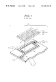
- FIGS. 1 and 2 there are shown a perspective view and a cross sectional view illustrating a three-level bolometer 100 , disclosed in U.S. application Ser. No. 09/102,364 entitled “BOLOMETER HAVING AN INCREASED FILL FACTOR”.
- the bolometer 100 comprises an active matrix level 110 , a support level 120 , at least a pair of posts 170 and an absorption level 130 .
- the active matrix level 110 has a substrate 112 including an integrated circuit (not shown), a pair of connecting terminals 114 and a protective layer 116 .
- Each of the connecting terminals 114 made of a metal is located on top of the substrate 112 .
- the pair of connecting terminals 114 are electrically connected to the integrated circuit.
- the support level 120 includes a pair of bridges 140 made of silicon nitride (SiN x ), each of the bridges 140 having a conduction line 165 formed on top thereof.
- Each of the bridges 140 is provided with an anchor portion 142 , a leg portion 144 and an elevated portion 146 , the anchor portion 142 including a via hole 152 through which one end of the conduction line 165 is electrically connected to the connecting terminal 114 , the leg portion 144 supporting the elevated portion 146 .
- the absorption level 130 is provided with a serpentine bolometer element 185 made of titanium (Ti), an absorber 195 made of silicon nitride (SiN x ) and an IR absorber coating 197 formed on top of the absorber 195 .
- the absorber 195 is fabricated by depositing silicon nitride before and after the formation of the serpentine bolometer element 185 to surround the serpentine bolometer element 185 .
- Each of the posts 170 is placed between the absorption level 130 and the support level 120 .
- Each of the posts 170 includes an electrical conduit 172 made of a metal, e.g., titanium (Ti), and surrounded by an insulating material 174 made of, e.g., silicon nitride (SiN x ).
- Top end of the electrical conduit 172 is electrically connected to one end of the serpentine bolometer element 185 and bottom end of the electrical conduit 172 is electrically connected to the conduction line 165 on the bridge 140 , in such a way that both ends of the serpentine bolometer element 185 in the absorption level 130 is electrically connected to the integrated circuit of the active matrix level 110 through the electrical conduits 172 , the conduction lines 165 and the connecting terminals 114 .
- the resistivity of the serpentine bolometer element 185 changes, causing a current and a voltage to vary, accordingly.
- the varied current or voltage is amplified by the integrated circuit, in such a way that the amplified current or voltage is read out by a detective circuit (not shown).
- a primary object of the present invention to provide a three-level infra-red bolometer including an absorber made of a material that can be formed at a low temperature and has a low heat-conductivity.
- a three-level infra-red bolometer which comprises: an active matrix level including a substrate and at least a pair of connecting terminals; a support level provided with at least a pair of bridges, each of the bridges including an conduction line, one end of the conduction line being electrically connected to the respective connecting terminal; an absorption level including a bolometer element formed between an upper absorber and a lower absorber, the absorbers being made of silicon oxide or silicon oxy-nitride; and at least a pair of posts, each of the posts being placed between the absorption level and the support level and including an electrical conduit surrounded by an insulating material, each end of the bolometer element of the absorption level being electrically connected to the respective connecting terminal through the respective electrical conduit and the respective conduction line.
- FIG. 1 shows a perspective view setting forth an infra-red bolometer previous disclosed
- FIG. 2 present a schematic cross sectional view depicting the infra-red bolometer shown in FIG. 1;
- FIG. 3 depicts a schematic cross sectional view setting forth a three-level infra-red bolometer in accordance with the present invention.
- FIGS. 4A to 4 B provide schematic cross sectional views depicting an absorption level in accordance with two preferred embodiments of present invention, respectively.
- FIGS. 3 and 4A to 4 B a schematic cross sectional view setting forth a three-level infra-red bolometer 200 and schematic cross sectional views of an absorption level therein in accordance with two embodiments of the present invention, respectively. It should be noted that like parts appearing in FIGS. 3 and 4A to 4 B are represented by like reference numerals.
- the inventive bolometer 200 shown in FIG. 3 comprises an active matrix level 210 , a support level 220 , at least a pair of posts 270 and an absorption level 230 .
- the active matrix level 210 has a substrate 212 including an integrated circuit (not shown), a pair of connecting terminals 214 and a protective layer 216 .
- Each of the connecting terminals 214 made of a metal is located on top of the substrate 212 .
- the pair of connecting terminals 214 are electrically connected to the integrated circuit.
- the protective layer 216 made of, e.g., silicon nitride (SiN x ) covers the substrate 212 .
- the support level 220 includes a pair of bridges 240 made of an insulating material, e.g., silicon oxide (SiO 2 ) or silicon oxy-nitride (SiO x N y ), each of the bridges 240 having a conduction line 265 formed on top thereof.
- Each of the bridges 240 is provided with an anchor portion 242 , a leg portion 244 and an elevated portion 246 , the anchor portion 242 including a via hole 252 through which one end of the conduction line 265 is electrically connected to the connecting terminal 214 , the leg portion 244 supporting the elevated portion 246 .
- the absorption level 230 is provided with an absorber 295 made of an insulating material, a serpentine bolometer element 285 made of a metal, e.g., titanium (Ti), and an IR absorber coating 297 positioned on top of the absorber 295 .
- an absorber 295 made of an insulating material
- a serpentine bolometer element 285 made of a metal, e.g., titanium (Ti)
- an IR absorber coating 297 positioned on top of the absorber 295 .
- the table below provides the deposition-temperature and heat-conductivity for the materials that can be used as the material for the absorber 295 .
- the absorber 295 includes a lower part 310 and an upper part 320 which are made of an insulating material, e.g., silicon oxide (SiO 2 ) or silicon oxy-nitride (SiO x N y ), as shown in FIG. 4 A.
- an insulating material e.g., silicon oxide (SiO 2 ) or silicon oxy-nitride (SiO x N y ), as shown in FIG. 4 A.
- a second embodiment is similar to the first embodiment, except that an upper and a lower parts 310 , 320 consist of two layers.
- the lower part 310 includes a first lower portion 312 made of silicon oxy-nitride (SiO x N y ) and a second lower portion 314 made of silicon oxide (SiO 2 ).
- the upper part 320 includes a first upper portion 322 made of silicon oxide (SiO 2 ) and a second upper portion 324 made of silicon oxy-nitride (SiO x N y ).
- Each of the posts 270 is placed between the absorption level 230 and the support level 220 .
- Each of the post 270 includes an electrical conduit 272 made of a metal, e.g., titanium (Ti) and surrounded by an insulating material 274 made of, e.g., silicon nitride (SiN x ).
- Top end of the electrical conduit 272 is electrically connected to one end of the serpentine bolometer element 285 and bottom end of the electrical conduit 272 is electrically connected to the conduction line 265 on the bridge 240 , in such a way that both ends of the serpentine bolometer element 285 in the absorption level 230 is electrically connected to the integrated circuit of the active matrix level 210 through the electrical conduits 272 , the conduction lines 265 and the connecting terminals 214 .
- the resistivity of the serpentine bolometer element 285 is increased, in such a way that the increased resistivity is read out by a detective circuit (not shown).
- the absorber 295 is made of a material having a relatively low heat conductivity and low deposition temperature, e.g., siliconoxide (SiO 2 ) or silicon oxy-nitride (SiO x N y ).
- the low deposition temperature will prevent the bolometer element from getting oxidized during the formation thereof and the low conductivity will increase the thermal isolation effect of the absorber 295 , which will, in turn, facilitate in ensuring an optimum performance of the bolometer 200 , e.g., a responsivity, a detectivity and a noise equilibrium temperature difference (NETD).
- NETD noise equilibrium temperature difference
Landscapes
- Physics & Mathematics (AREA)
- General Physics & Mathematics (AREA)
- Spectroscopy & Molecular Physics (AREA)
- Photometry And Measurement Of Optical Pulse Characteristics (AREA)
- Radiation Pyrometers (AREA)
Abstract
Description
| deposition- | heat-conductivity | |||
| material | temperature(° C.) | (W/m · ° C.) | ||
| SiNx | 850 | 19 | ||
| SiO2 | 200 | 1.3-1.8 | ||
| SiOxNy | 300 | 10.1-10.4 | ||
Claims (5)
Priority Applications (2)
| Application Number | Priority Date | Filing Date | Title |
|---|---|---|---|
| PCT/KR1998/000266 WO2000012985A1 (en) | 1998-08-31 | 1998-08-31 | Bolometer including an absorber made of a material having a low deposition-temperature and a low heat-conductivity |
| US09/146,256 US6201244B1 (en) | 1998-08-31 | 1998-09-03 | Bolometer including an absorber made of a material having a low deposition-temperature and a low heat-conductivity |
Applications Claiming Priority (2)
| Application Number | Priority Date | Filing Date | Title |
|---|---|---|---|
| PCT/KR1998/000266 WO2000012985A1 (en) | 1998-08-31 | 1998-08-31 | Bolometer including an absorber made of a material having a low deposition-temperature and a low heat-conductivity |
| US09/146,256 US6201244B1 (en) | 1998-08-31 | 1998-09-03 | Bolometer including an absorber made of a material having a low deposition-temperature and a low heat-conductivity |
Publications (1)
| Publication Number | Publication Date |
|---|---|
| US6201244B1 true US6201244B1 (en) | 2001-03-13 |
Family
ID=26633371
Family Applications (1)
| Application Number | Title | Priority Date | Filing Date |
|---|---|---|---|
| US09/146,256 Expired - Lifetime US6201244B1 (en) | 1998-08-31 | 1998-09-03 | Bolometer including an absorber made of a material having a low deposition-temperature and a low heat-conductivity |
Country Status (2)
| Country | Link |
|---|---|
| US (1) | US6201244B1 (en) |
| WO (1) | WO2000012985A1 (en) |
Cited By (4)
| Publication number | Priority date | Publication date | Assignee | Title |
|---|---|---|---|---|
| KR20030016867A (en) * | 2001-08-22 | 2003-03-03 | 대우전자주식회사 | Method for forming a silicon oxide layer in an infrared bolometer |
| US20040202742A1 (en) * | 2001-07-23 | 2004-10-14 | Winter Amos G | Continuous foam core laminating machine for construction panels |
| US6838669B1 (en) | 2002-04-25 | 2005-01-04 | The United States Of America As Represented By The Administrator Of The National Aeronautics And Space Administration | Wide operational range thermal sensor |
| US20060054823A1 (en) * | 2004-09-16 | 2006-03-16 | Commissariat A I'energie Atomique | Thermal electromagnetic radiation detector comprising an absorbent membrane fixed in suspension |
Families Citing this family (3)
| Publication number | Priority date | Publication date | Assignee | Title |
|---|---|---|---|---|
| US6621083B2 (en) * | 2000-12-29 | 2003-09-16 | Honeywell International Inc. | High-absorption wide-band pixel for bolometer arrays |
| US9029783B2 (en) * | 2011-06-10 | 2015-05-12 | Flir Systems, Inc. | Multilayered microbolometer film deposition |
| EP3938746A2 (en) | 2019-03-11 | 2022-01-19 | Flir Commercial Systems, Inc. | Microbolometer systems and methods |
Citations (13)
| Publication number | Priority date | Publication date | Assignee | Title |
|---|---|---|---|---|
| US5021663A (en) * | 1988-08-12 | 1991-06-04 | Texas Instruments Incorporated | Infrared detector |
| EP0534768A1 (en) | 1991-09-27 | 1993-03-31 | Texas Instruments Incorporated | Uncooled infrared detector and method for forming the same |
| US5286976A (en) * | 1988-11-07 | 1994-02-15 | Honeywell Inc. | Microstructure design for high IR sensitivity |
| US5397897A (en) * | 1992-04-17 | 1995-03-14 | Terumo Kabushiki Kaisha | Infrared sensor and method for production thereof |
| US5404125A (en) * | 1991-07-19 | 1995-04-04 | Terumo Kabushiki Kaisha | Infrared radiation sensor |
| US5572029A (en) | 1994-06-30 | 1996-11-05 | Walker; William K. | Thermal isolation for hybrid thermal detectors |
| US5629521A (en) * | 1995-12-11 | 1997-05-13 | Industrial Technology Research Institute | Interferometer-based bolometer |
| US5760398A (en) * | 1995-12-04 | 1998-06-02 | Lockheed Martin Ir Imaging Systems, Inc. | Infrared radiation detector having a reduced active area |
| US5789753A (en) * | 1995-07-21 | 1998-08-04 | Texas Instruments Incorporated | Stress tolerant bolometer |
| US5811815A (en) * | 1995-11-15 | 1998-09-22 | Lockheed-Martin Ir Imaging Systems, Inc. | Dual-band multi-level microbridge detector |
| US5939971A (en) * | 1998-07-14 | 1999-08-17 | Daewoo Electronics Co., Ltd. | Infrared bolometer |
| US6028312A (en) * | 1995-07-21 | 2000-02-22 | Texas Instruments Incorporated | Electronic chopping |
| US6034374A (en) * | 1996-11-08 | 2000-03-07 | Nikon Corporation | Thermal infrared sensors, imaging devices, and manufacturing methods for such sensors |
-
1998
- 1998-08-31 WO PCT/KR1998/000266 patent/WO2000012985A1/en not_active Ceased
- 1998-09-03 US US09/146,256 patent/US6201244B1/en not_active Expired - Lifetime
Patent Citations (14)
| Publication number | Priority date | Publication date | Assignee | Title |
|---|---|---|---|---|
| US5021663B1 (en) * | 1988-08-12 | 1997-07-01 | Texas Instruments Inc | Infrared detector |
| US5021663A (en) * | 1988-08-12 | 1991-06-04 | Texas Instruments Incorporated | Infrared detector |
| US5286976A (en) * | 1988-11-07 | 1994-02-15 | Honeywell Inc. | Microstructure design for high IR sensitivity |
| US5404125A (en) * | 1991-07-19 | 1995-04-04 | Terumo Kabushiki Kaisha | Infrared radiation sensor |
| EP0534768A1 (en) | 1991-09-27 | 1993-03-31 | Texas Instruments Incorporated | Uncooled infrared detector and method for forming the same |
| US5397897A (en) * | 1992-04-17 | 1995-03-14 | Terumo Kabushiki Kaisha | Infrared sensor and method for production thereof |
| US5572029A (en) | 1994-06-30 | 1996-11-05 | Walker; William K. | Thermal isolation for hybrid thermal detectors |
| US5789753A (en) * | 1995-07-21 | 1998-08-04 | Texas Instruments Incorporated | Stress tolerant bolometer |
| US6028312A (en) * | 1995-07-21 | 2000-02-22 | Texas Instruments Incorporated | Electronic chopping |
| US5811815A (en) * | 1995-11-15 | 1998-09-22 | Lockheed-Martin Ir Imaging Systems, Inc. | Dual-band multi-level microbridge detector |
| US5760398A (en) * | 1995-12-04 | 1998-06-02 | Lockheed Martin Ir Imaging Systems, Inc. | Infrared radiation detector having a reduced active area |
| US5629521A (en) * | 1995-12-11 | 1997-05-13 | Industrial Technology Research Institute | Interferometer-based bolometer |
| US6034374A (en) * | 1996-11-08 | 2000-03-07 | Nikon Corporation | Thermal infrared sensors, imaging devices, and manufacturing methods for such sensors |
| US5939971A (en) * | 1998-07-14 | 1999-08-17 | Daewoo Electronics Co., Ltd. | Infrared bolometer |
Non-Patent Citations (1)
| Title |
|---|
| International Search Report Apr. 9, 1999. |
Cited By (5)
| Publication number | Priority date | Publication date | Assignee | Title |
|---|---|---|---|---|
| US20040202742A1 (en) * | 2001-07-23 | 2004-10-14 | Winter Amos G | Continuous foam core laminating machine for construction panels |
| KR20030016867A (en) * | 2001-08-22 | 2003-03-03 | 대우전자주식회사 | Method for forming a silicon oxide layer in an infrared bolometer |
| US6838669B1 (en) | 2002-04-25 | 2005-01-04 | The United States Of America As Represented By The Administrator Of The National Aeronautics And Space Administration | Wide operational range thermal sensor |
| US20060054823A1 (en) * | 2004-09-16 | 2006-03-16 | Commissariat A I'energie Atomique | Thermal electromagnetic radiation detector comprising an absorbent membrane fixed in suspension |
| US7294836B2 (en) * | 2004-09-16 | 2007-11-13 | Commissariat A L'energie Atomique | Thermal electromagnetic radiation detector comprising an absorbent membrane fixed in suspension |
Also Published As
| Publication number | Publication date |
|---|---|
| WO2000012985A1 (en) | 2000-03-09 |
Similar Documents
| Publication | Publication Date | Title |
|---|---|---|
| JP7232978B2 (en) | Method for Cooling Infrared Sensors and Bolometer Infrared Receivers of Infrared Sensors | |
| JP2834202B2 (en) | Infrared detector | |
| US5367167A (en) | Uncooled infrared detector and method for forming the same | |
| US5912464A (en) | Infrared detector and manufacturing process | |
| US5939971A (en) | Infrared bolometer | |
| US6094127A (en) | Infrared bolometer and method for manufacturing same | |
| US6201244B1 (en) | Bolometer including an absorber made of a material having a low deposition-temperature and a low heat-conductivity | |
| US6198099B1 (en) | Bolometer including a reflective layer | |
| JP2526247B2 (en) | Thermopile | |
| US6262417B1 (en) | Infrared bolometer | |
| US3745360A (en) | Radiation circuit radiation detector | |
| US6242738B1 (en) | Structurally stable infrared bolometer | |
| EP1131612B1 (en) | Bolometer including an absorber made of a material having a low deposition-temperature and a low heat-conductivity | |
| EP1137918B1 (en) | Infrared bolometer | |
| EP1117978B1 (en) | Bolometer with a serpentine stress balancing member | |
| KR100299642B1 (en) | Three-level infra-red bolometer | |
| JP3396719B2 (en) | Infrared bolometer | |
| EP1161660B1 (en) | Bolometer with a zinc oxide bolometer element | |
| EP1144967B1 (en) | Structurally stable infrared bolometer | |
| WO2000003214A1 (en) | Bolometer having an increased fill factor | |
| JPH046424A (en) | Infrared sensor | |
| EP1131613B1 (en) | Bolometer including a reflective layer | |
| EP1141669B1 (en) | Infrared bolometer and method for manufacturing same | |
| WO2000033032A1 (en) | Infrared bolometer with an enhanced structural stability and integrity | |
| KR100529133B1 (en) | Infrared rays absorption bolometer |
Legal Events
| Date | Code | Title | Description |
|---|---|---|---|
| AS | Assignment |
Owner name: DAEWOO ELECTRONICS CO., LTD., KOREA, REPUBLIC OF Free format text: ASSIGNMENT OF ASSIGNORS INTEREST;ASSIGNORS:JU, SANG-BAEK;YONG, YOON-JOONG;REEL/FRAME:009438/0597 Effective date: 19980825 |
|
| FEPP | Fee payment procedure |
Free format text: PAYOR NUMBER ASSIGNED (ORIGINAL EVENT CODE: ASPN); ENTITY STATUS OF PATENT OWNER: LARGE ENTITY |
|
| STCF | Information on status: patent grant |
Free format text: PATENTED CASE |
|
| AS | Assignment |
Owner name: DAEWOO ELECTRONICS CORPORATION, KOREA, REPUBLIC OF Free format text: ASSIGNMENT OF ASSIGNORS INTEREST;ASSIGNOR:DAEWOO ELECTRONICS CO., LTD.;REEL/FRAME:014363/0688 Effective date: 20030517 |
|
| FPAY | Fee payment |
Year of fee payment: 4 |
|
| FPAY | Fee payment |
Year of fee payment: 8 |
|
| FEPP | Fee payment procedure |
Free format text: PAYOR NUMBER ASSIGNED (ORIGINAL EVENT CODE: ASPN); ENTITY STATUS OF PATENT OWNER: LARGE ENTITY Free format text: PAYER NUMBER DE-ASSIGNED (ORIGINAL EVENT CODE: RMPN); ENTITY STATUS OF PATENT OWNER: LARGE ENTITY |
|
| AS | Assignment |
Owner name: MAPLE VISION TECHNOLOGIES INC., CANADA Free format text: ASSIGNMENT OF ASSIGNORS INTEREST;ASSIGNOR:DAEWOO ELECTRONICS CORPORATION;REEL/FRAME:027437/0446 Effective date: 20111215 |
|
| FPAY | Fee payment |
Year of fee payment: 12 |
|
| AS | Assignment |
Owner name: QUARTERHILL INC., CANADA Free format text: MERGER AND CHANGE OF NAME;ASSIGNORS:MAPLE VISION TECHNOLOGIES INC.;QUARTERHILL INC.;REEL/FRAME:042936/0517 Effective date: 20170601 |
|
| AS | Assignment |
Owner name: WI-LAN INC., CANADA Free format text: ASSIGNMENT OF ASSIGNORS INTEREST;ASSIGNOR:QUARTERHILL INC.;REEL/FRAME:043181/0101 Effective date: 20170601 |