US6171733B1 - Material for forming black matrix for color liquid crystal display and method for forming black matrix - Google Patents
Material for forming black matrix for color liquid crystal display and method for forming black matrix Download PDFInfo
- Publication number
- US6171733B1 US6171733B1 US09/359,393 US35939399A US6171733B1 US 6171733 B1 US6171733 B1 US 6171733B1 US 35939399 A US35939399 A US 35939399A US 6171733 B1 US6171733 B1 US 6171733B1
- Authority
- US
- United States
- Prior art keywords
- black matrix
- carbon atoms
- alkyl group
- liquid crystal
- crystal display
- Prior art date
- Legal status (The legal status is an assumption and is not a legal conclusion. Google has not performed a legal analysis and makes no representation as to the accuracy of the status listed.)
- Expired - Lifetime
Links
Classifications
-
- G—PHYSICS
- G02—OPTICS
- G02F—OPTICAL DEVICES OR ARRANGEMENTS FOR THE CONTROL OF LIGHT BY MODIFICATION OF THE OPTICAL PROPERTIES OF THE MEDIA OF THE ELEMENTS INVOLVED THEREIN; NON-LINEAR OPTICS; FREQUENCY-CHANGING OF LIGHT; OPTICAL LOGIC ELEMENTS; OPTICAL ANALOGUE/DIGITAL CONVERTERS
- G02F1/00—Devices or arrangements for the control of the intensity, colour, phase, polarisation or direction of light arriving from an independent light source, e.g. switching, gating or modulating; Non-linear optics
- G02F1/01—Devices or arrangements for the control of the intensity, colour, phase, polarisation or direction of light arriving from an independent light source, e.g. switching, gating or modulating; Non-linear optics for the control of the intensity, phase, polarisation or colour
- G02F1/13—Devices or arrangements for the control of the intensity, colour, phase, polarisation or direction of light arriving from an independent light source, e.g. switching, gating or modulating; Non-linear optics for the control of the intensity, phase, polarisation or colour based on liquid crystals, e.g. single liquid crystal display cells
- G02F1/133—Constructional arrangements; Operation of liquid crystal cells; Circuit arrangements
- G02F1/1333—Constructional arrangements; Manufacturing methods
- G02F1/1335—Structural association of cells with optical devices, e.g. polarisers or reflectors
- G02F1/133509—Filters, e.g. light shielding masks
- G02F1/133512—Light shielding layers, e.g. black matrix
-
- G—PHYSICS
- G03—PHOTOGRAPHY; CINEMATOGRAPHY; ANALOGOUS TECHNIQUES USING WAVES OTHER THAN OPTICAL WAVES; ELECTROGRAPHY; HOLOGRAPHY
- G03F—PHOTOMECHANICAL PRODUCTION OF TEXTURED OR PATTERNED SURFACES, e.g. FOR PRINTING, FOR PROCESSING OF SEMICONDUCTOR DEVICES; MATERIALS THEREFOR; ORIGINALS THEREFOR; APPARATUS SPECIALLY ADAPTED THEREFOR
- G03F7/00—Photomechanical, e.g. photolithographic, production of textured or patterned surfaces, e.g. printing surfaces; Materials therefor, e.g. comprising photoresists; Apparatus specially adapted therefor
- G03F7/0005—Production of optical devices or components in so far as characterised by the lithographic processes or materials used therefor
- G03F7/0007—Filters, e.g. additive colour filters; Components for display devices
-
- G—PHYSICS
- G03—PHOTOGRAPHY; CINEMATOGRAPHY; ANALOGOUS TECHNIQUES USING WAVES OTHER THAN OPTICAL WAVES; ELECTROGRAPHY; HOLOGRAPHY
- G03F—PHOTOMECHANICAL PRODUCTION OF TEXTURED OR PATTERNED SURFACES, e.g. FOR PRINTING, FOR PROCESSING OF SEMICONDUCTOR DEVICES; MATERIALS THEREFOR; ORIGINALS THEREFOR; APPARATUS SPECIALLY ADAPTED THEREFOR
- G03F7/00—Photomechanical, e.g. photolithographic, production of textured or patterned surfaces, e.g. printing surfaces; Materials therefor, e.g. comprising photoresists; Apparatus specially adapted therefor
- G03F7/004—Photosensitive materials
- G03F7/038—Macromolecular compounds which are rendered insoluble or differentially wettable
-
- G—PHYSICS
- G03—PHOTOGRAPHY; CINEMATOGRAPHY; ANALOGOUS TECHNIQUES USING WAVES OTHER THAN OPTICAL WAVES; ELECTROGRAPHY; HOLOGRAPHY
- G03F—PHOTOMECHANICAL PRODUCTION OF TEXTURED OR PATTERNED SURFACES, e.g. FOR PRINTING, FOR PROCESSING OF SEMICONDUCTOR DEVICES; MATERIALS THEREFOR; ORIGINALS THEREFOR; APPARATUS SPECIALLY ADAPTED THEREFOR
- G03F7/00—Photomechanical, e.g. photolithographic, production of textured or patterned surfaces, e.g. printing surfaces; Materials therefor, e.g. comprising photoresists; Apparatus specially adapted therefor
- G03F7/004—Photosensitive materials
- G03F7/0048—Photosensitive materials characterised by the solvents or agents facilitating spreading, e.g. tensio-active agents
Definitions
- the present invention relates to a material for forming a black matrix for a color liquid crystal display and a method for forming a black matrix for a color liquid crystal display using the same.
- the color filter for a color liquid crystal display influences the displaying grade of the color liquid crystal display. Above all, it is essential that a black matrix for a color filter not only have sufficient light-shielding ability but also be formed with high resolution for achieving a high opening factor and high contrast.
- Chromium-deposited films have so far been used in black matrices for a color filter.
- black matrices comprising a chromium-deposited film are excellent in light-shielding ability, they have several problems that ghost image is caused as they have a high reflection coefficient leading to the deterioration of visibility, the color filter manufacturing process in which chromium is used in a black matrix is complicated and expensive, and the disposal of chromium waste solutions is problematic.
- black matrices comprising a photosensitive resin film having dispersed therein a black pigment and patterned upon a design have been developed. These black matrices have a low reflection coefficient and can be manufactured inexpensively.
- a radical polymerization type photosensitive resin is used as this photosensitive resin having dispersed therein a black pigment, but a radical polymerization type photosensitive resin is barely hardened in the range where a light reaches, therefore, hardening becomes insufficient in the vicinity of the interface between the film and the substrate. As a result, the development latitude becomes narrow.
- An object of the present invention is to provide a black matrix-forming material for a color liquid crystal display in which a hardening reaction proceeds sufficiently to the interface with the substrate even with a high concentration of a black pigment and which can provide wide development latitude.
- a further object of the present invention is to provide a black matrix-forming material for a color liquid crystal display in which a hardening reaction does not proceed by merely blending, coating and drying the components constituting the black matrix-forming material, the solubility contrast of the exposed area and the unexposed area to the developing solution is sufficiently large, and from which a highly accurate black matrix can be produced.
- Another object of the present invention is to provide a method for forming a black matrix for a color liquid crystal display of high concentration and high accuracy.
- a material for forming a black matrix for a color liquid crystal display comprising:
- R 1 represents a straight chain or branched alkyl group having from 1 to 24 carbon atoms, and this alkyl group may have a substituent
- R 2 and R 3 each represents a hydrogen atom or a methyl group
- R 4 represents a hydrogen atom, a straight chain or branched alkyl group having from 1 to 24 carbon atoms, —COR 5 or —CONR 6 , and this alkyl group may have a substituent
- R 5 and R 6 each represents an alkyl group having from 1 to 12 carbon atoms, an aryl group having from 6 to 12 carbon atoms, or an alkenyl group having from 6 to 32 carbon atoms
- m represents 0, 1 or 2
- n represents 1, 2 or 3, provided that m+n is 3
- a and b each represents a number of from 0 to 200, provided that a+b is from 2 to 200; and
- a method for forming a black matrix for a color liquid crystal display which comprises coating the above black matrix-forming material for a color liquid crystal display on a transparent substrate, subjecting the film formed to exposure of the prescribed patterning, heat treating the film to effect crosslinking of the exposed area and distributing the acid generated by the exposure to the substrate, and then removing the unexposed area by alkali development.
- the component (C) present on the exposed area is thereby decomposed to generate an acid.
- the above generated acid crosslinks an acid-crosslinkable methylolated melamine compound, component (B), and makes it insoluble to an alkali developing solution, at the same time, the acid generated by the exposure diffuses to the substrate and also crosslinks and insolubilizes component (B) present near the substrate.
- component (B) is crosslinked far to the interface between the film and the substrate only by the exposure of the film surface and can be insolubilized to a developing solution.
- a black matrix containing a black pigment in high concentration can be formed.
- black pigments so far been used, there have been such problems as an alkali-insoluble substance is formed by merely blending, coating and drying a black pigment with components (A), (B) and (C), and the composition becomes substantially developing solution-insoluble and patterning cannot be effected.
- the black matrix-forming material containing components (A), (B), (C), (D) and (E) in the present invention does not cause such problems.
- an alkali-soluble resin obtained by the condensation reaction of phenols containing at least cresol with aldehydes, which is component (A) of the black matrix-forming material for the color liquid crystal display according to the present invention, is described below.
- resol resins or novolak resins obtained by the condensation reaction of phenols containing at least cresol with aldehydes are preferably used.
- alkali-soluble resins obtained by the condensation reaction of phenols containing at least cresol with aldehydes resins obtained by the reaction of phenols containing 50 mol% or more of o-, m- or p-cresol with aldehydes are preferably used.
- phenols which may be contained other than cresol include o-methoxyphenol, m-methoxyphenol, o-ethylphenol, m-ethylphenol, p-ethylphenol, 3,5-dimethoxyphenol, 2-methoxy-4-methylphenol, o-propoxyphenol, o-butoxyphenol, 3,4,5-trimethylphenol, o-vinylphenol, and m-phenylphenol.
- aldehydes examples include formaldehyde, paraformaldehyde, acetaldehyde, propylaldehyde, benzaldehyde, phenylaldehyde, ⁇ -phenylpropylaldehyde, ⁇ -phenylpropylaldehyde, and o-hydroxybenzaldehyde.
- formaldehyde is preferred.
- Resins obtained by the reaction of o-, m- or p-cresol or mixtures of them with formaldehyde are preferably used in the present invention.
- These resins preferably have weight average molecular weight of from 500 to 20,000, and more preferably from 1,000 to 15,000.
- the content of alkali-soluble resin component (A) in the black matrix-forming material according to the present invention is preferably from 35 to 90 wt %, more preferably from 45 to 75 wt %, based on the total solid content (by weight).
- acid-crosslinkable methylolated melamine compounds include monomethylolmelamine, dimethylolmelamine, trimethylolmelamine, tetramethylolmelamine, pentamethylolmelamine, and hexamethylolmelamine, and hexamethylolmelamine is preferably used in the present invention.
- the content of the acid-crosslinkable methylolated melamine compound, component (B), in the black matrix-forming material according to the present invention is preferably from 0.1 to 30 wt %, more preferably from 1 to 10 wt %, based on the total solid content (by weight).
- a compound which absorbs a light and then generates an acid (a light-acid generating agent), which is component (C) of the black matrix-forming material for the color liquid crystal display according to the present invention, is described below.
- a light-acid generating agent generally known onium salts, quinonediazide compounds, or organic halides can be used.
- onium salts e.g., diazonium salts, phosphonium salts and sulfonium salts having a fluoroborate anion, a trifluoromethanesulfonate anion, a paratoluenesulfonate anion, or a paranitrotoluenesulfonate anion as a counter ion.
- onium salts e.g., diazonium salts, phosphonium salts and sulfonium salts having a fluoroborate anion, a trifluoromethanesulfonate anion, a paratoluenesulfonate anion, or a paranitrotoluenesulfonate anion as a counter ion.
- an organic halide means a compound which forms hydroacid halide, e.g., compounds disclosed in U.S. Pat. Nos. 351,552, 536,489, 3,779,778, and West German Patent Application (OLS) No. 2,243,621 can be exemplified. More specifically, those compounds disclosed in U.S. Pat. No.
- 351,552 e.g., carbon tetrabromide, tetra(bromomethyl)methane, tetrabromoethylene, 1,2,3,4-tetrabromobutane, trichloroethoxyethanol, p-iodophenol, p-bromophenol, p-iodobiphenyl, 2,6-dibromophenol, 1-bromo-2-naphthol, p-bromoaniline, hexachloro-p-xylene, trichloroacetanilide, p-bromodimethylaniline, tetrachlorotetrahydronaphthalene, a,a′-dibromoxylene, a,a,a,a′-tetrabromoxylene, hexabromoethane, 1-chloroanthraquinone, ⁇ , ⁇ , ⁇ -tribromoquinaldine, hexa
- Pat. No. 3,779,778, e.g., hexabromoethane, a,a,a-trichloroacetophenone, tribromotrichloroethane and halomethyl-s-triazines can be exemplified.
- halomethyl-s-triazines e.g., 2,4-bis-(trichloromethyl)-6-methyl-s-triazine and 2,4,6-tris-(trichloromethyl)-s-triazine are particularly preferred.
- compounds substituted with vinylhalomethyl-s-triazine disclosed in U.S. Patent 3,987,037 can be exemplified.
- This vinylhalomethyl-s-triazine compound is photolytic triazine having at least one trihalomethyl group and a group conjugated with a triazine ring by at least one ethylenically unsaturated bond, which is represented by the following formula (A):
- P represents —C(Q) 3 , —NH 2 , —NHR, —N(R) 2 , or —OR (wherein R represents a phenyl group or a lower alkyl group having 6 or less carbon atoms); Q represents bromine or chlorine; n represents an integer of from 1 to 3; and W represents an aromatic ring or a group represented by the following formula (B):
- Z represents oxygen or sulfur
- R 1 represents a lower alkyl group or a phenyl group.
- the aromatic ring or the heterocyclic ring represented by W may further be substituted, and examples of the substituents include chlorine, bromine, a phenyl group, a lower alkyl group having 6 or less carbon atoms, nitro, phenoxy, alkoxyl, acetoxy, acetyl, amino and alkylamino groups.
- the compounding amount of the light-acid generating agent, component (C), in the black matrix-forming material according to the present invention is preferably from 0.1 to 30 wt %, more preferably from 1 to 10 wt %, based on the total solid content (by weight).
- a straight chain or branched alkyl group having from 1 to 24 carbon atoms represented by R 1 and R 4 a straight chain or branched alkyl group having from 1 to 24 carbon atoms such as CH 3 —, CH 3 CH 2 —, CH 3 (CH 2 ) 2 —, CH 3 (CH 2 ) 3 —, CH 3 (CH 2 ) 4 —, (CH 3 ) 2 CH(CH 2 ) 2 —, CH 3 CH 2 CH(CH 3 )CH 2 —, CH 3 (CH 2 ) 2 CH(CH 3 )—, CH 3 (CH 2 ) 7 —, CH 3 (CH 2 ) 8 —, CH 3 (CH 2 ) 10 —, CH 3 (CH 2 ) 12 —, CH 3 (CH 2 ) 14 —, CH 3 (CH 2 ) 16 —, CH 3 (CH 2 ) 18 —, CH 3 (CH 2 ) 20 —, CH 3 (CH 2 ) 22 —, or CH 3 (CH 2 —,
- alkyl group having from 1 to 12 carbon atoms represented by R 5 and R 6 (when R 4 represents —COR 5 or —COR 6 ), the above-described examples of the alkyl groups having from 1 to 12 carbon atoms can be exemplified.
- aryl group having from 6 to 12 carbon atoms which may be substituted represented by R 5 and R 6 examples thereof include a monocyclic or bicyclic aryl group e.g., phenyl,
- alkenyl group having from 6 to 32 carbon atoms represented by R 5 , and R 6 the following can be exemplified:
- R 1 preferably represents a straight chain or branched alkyl group having from 1 to 12 carbon atoms
- R 2 preferably represents a hydrogen atom
- R 3 preferably represents a methyl group
- R 4 preferably represents a hydrogen atom or an alkyl group having from 1 to 8 carbon atoms
- a+b is preferably from 4 to 100, more preferably from 10 to 50.
- a dispersant represented by formula (I) preferably has:
- a molecular weight from 1 ⁇ 10 3 to 1 ⁇ 10 4
- the above dispersant has an acid value of from 0 to 5, preferably from 0 to 2; an amine value of from 20 to 40, preeferably from 25 to 35, and a molecular weight of from 1 ⁇ 10 3 to 1 ⁇ 10 4 , preferably from 1 ⁇ 10 3 to 5 ⁇ 10 3 .
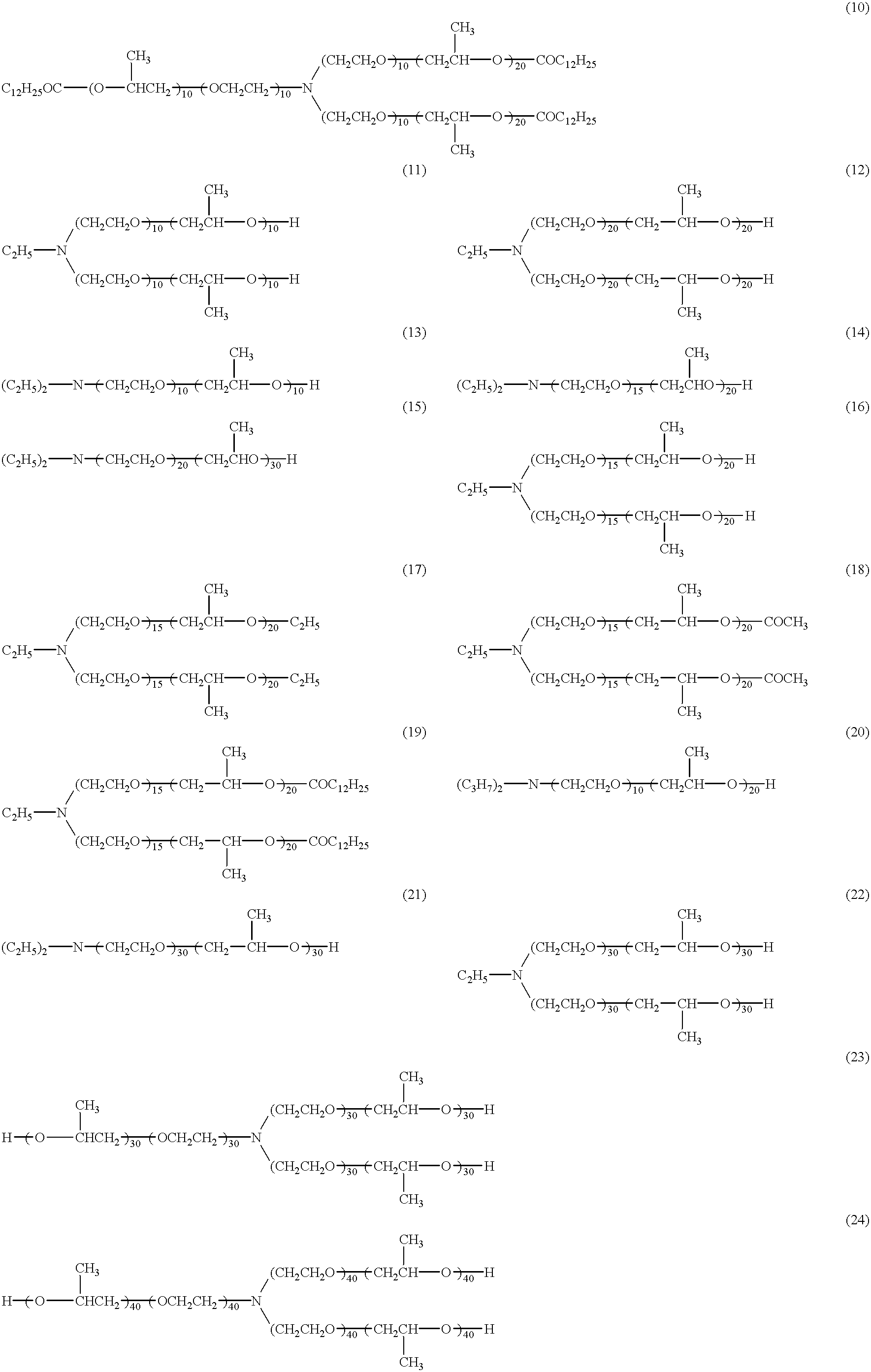
- dispersants represented by formula (I) are shown below, but the present invention is not restricted thereto.
- the content of the dispersant represented by formula (I), component (D), in the black matrix-forming material according to the present invention is preferably from 0.01 to 70 wt %, more preferably from 0.4 to 40 wt %, based on the total weight of pigments.
- the black pigment (E) for use in the present invention may be organic or inorganic.
- Examples of preferred organic pigments include pigments having high heat resistance and high light fastness such as phthalocyanine pigments, e.g., Phthalocyanine Blue and Phthalocyanine Green; anthraquinone pigments, e.g., Chromophthal Red; azo or azo-lake pigments, e.g., Bordeaux 10B and Lake Red; isoindolinone pigments, e.g., Irgazine Yellow; dioxazine pigments, e.g., Dioxazine Violet; nitroso pigments, e.g., Naphthol Green B; nitro pigments; lake pigments, e.g., Peacock Blue Lake and Rhodamine Lake; quinacridone pigments; and quinacridine pigments.
- phthalocyanine pigments e.g., Phthalocyanine Blue and Phthalocyanine Green
- anthraquinone pigments e.g., Chromophthal Red
- examples of preferred inorganic pigments include carbon black; metal oxide pigments, e.g., titanium oxide, iron oxide, zinc oxide and chromium oxide; sulfide pigments, e.g., zinc sulfide; and carbonate and silicate.
- These pigments can be used alone or in combination of two or more, although it depends on the kind of the pigment.
- the particle size of pigments is 0.4 ⁇ m or less, particularly preferably 0.2 ⁇ m or less.
- the ratio of the amount of pigments used such that the transmittance throughout the visible light region is uniformly 5% or less and the transmittance in the vicinity of 550 nm which is the most sensitive region to the human eyes becomes minimum.
- the content of the pigment in the black matrix-forming material according to the present invention is preferably from 10 to 70 wt %, particularly preferably from 20 to 50 wt %, based on the total solid content (by weight).
- the black matrix-forming material for the color liquid crystal display according to the present invention may contain optional components other than (A), (B), (C), (D) and (E) components such as a silicone surfactant, a fluorine surfactant, a polyether surfactant, amines, etc., in the range not impairing the achievement of the objects of the present invention.
- pigments are generally dispersed with a pigment dispersant in wet dispersing system but the following means can be used, if necessary.
- a black pigment is subjected to flashing process in the first place, and then kneaded with a resin by means of a kneader, an extruder, a ball mill or a double or triple roll mill.
- a method of first blending a black pigment and a resin homogeneously with adding a solvent, then sufficiently kneading the pigment and the resin with heating, if necessary, using a two- or three-roll mill to obtain a homogeneous colored product can be applied.
- the pigment and other constituting components including a dispersant are blended to effect wet dispersion (primary dispersion).
- the obtained dispersion solution is again subjected to wet dispersion (secondary dispersion) using finer beads until the pigment reaches the objective size distribution.
- the objective size and size distribution can be attained by separating the wet dispersed dispersion solution by centrifugation or removing coarse particles by decantation.
- the thus-obtained colored dispersion is mixed with components (B) and (C) and offered for use as a photo-sensitive composition.
- the black matrix for a color liquid crystal display can be formed from the black matrix-forming material of the present invention by the following procedure.
- the resist comprising the black matrix-forming material containing (A) an alkali-soluble resin, (B) an acid-crosslinkable methylolated melamine resin, (C) a light-acid generating agent, (D) a dispersant, (E) a black pigment, and optional components is coated on a transparent substrate, the solvent is dried by heating to form a black resist film.
- the black resist film is selectively exposed using a mask having a desired pattern.
- component (C) is decomposed by the action of the light and generates an acid at the exposed area on the surface of the resist.
- This acid and component (B) react by heat treatment and component (B) is crosslinked, at the same time, the acid diffuses in the thickness direction of the black resist film and the crosslinking of component (B) further proceeds to the vicinity of the substrate, thereby a latent image is formed.
- development processing is performed using an alkali developing solution to remove the unexposed area, as a result, a black resist pattern is selectively formed on the transparent substrate.
- a black matrix is formed.
- the film thickness of the above coated film is preferably from 0.5 to 5 ⁇ m, more preferably from 0.7 to 3 ⁇ m.
- Ultraviolet rays, electron beams or X-rays are used for the above-described exposure light source.
- the temperature for the above heat treatment is preferably from 80 to 180° C., more preferably from 100 to 160° C., and the heating time is preferably from 30 to 300 seconds, more preferably from 30 to 180 seconds.
- Alkali developing solutions which are usually used in this field can be used as the alkali developing solution, e.g., inorganic alkalis such as potassium hydroxide, sodium hydroxide, potassium carbonate, sodium carbonate, potassium hydrogencarbonate, and sodium hydrogencarbonate, and amines such as triethanolamine, trimethylamine, triethylamine, pyridine, tetramethylammonium hydroxide, and tetraethylammonium hydroxide can be exemplified as such alkali developing solutions.
- inorganic alkalis such as potassium hydroxide, sodium hydroxide, potassium carbonate, sodium carbonate, potassium hydrogencarbonate, and sodium hydrogencarbonate
- amines such as triethanolamine, trimethylamine, triethylamine, pyridine, tetramethylammonium hydroxide, and tetraethylammonium hydroxide can be exemplified as such alkali developing solutions.
- the black matrix-forming material according to the present invention When the black matrix-forming material according to the present invention is used as a resist, an acid is generated upon exposure. After that, a crosslinking reaction occurs selectively by heat treatment on the area where an acid has been generated and, at the same time, and the acid further diffuses in the thickness direction of the resist to accelerate the hardening of the resist, thereby a black matrix having wide development latitude and high optical density can be formed.
- a solution having the following composition was prepared in the first place and the solution was stirred for 8 hours to obtain a photosensitive resin solution.
- This photosensitive resin solution was coated on a substrate by means of a spin coater in a film thickness of 1.0 ⁇ m and heated at 100° C. for 60 seconds.
- the substrate was prepared by cutting borosilicate glass 7059 (manufactured by Corning Co.) having a thickness of 1.1 mm to 100 mm square and subjecting the square glass to ultrasonic cleaning using a 1%-sodium hydroxide aqueous solution.
- the coated substrate was exposed through a mask having a line width of 20 ⁇ m (the dimension of the part to become a black matrix was 20 ⁇ m) using an exposer (manufactu red by Ushio Electric Co. Ltd.) at 200 Mj/cm 2 .
- the substrate was subjected to development consisting of heating at 130° C. for 60 seconds, immersing in a developing solution FHD-5 (manufactured by FUJIFILM OLIN Co., Ltd.), and then washing by high pressure spraying.
- FHD-5 manufactured by FUJIFILM OLIN Co., Ltd.
- the film thickness was 1.04 ⁇ m and optical density (OD) was 3.15.
- OD optical density
- Black matrix-forming materials were prepared in the same manner as in Example 1 except for replacing the dispersant used in Example 1 with those described in Table 1 below and evaluation was performed in the same manner as above. The film thickness and optical density of each sample obtained are shown in Table 1 below. Black matrix-forming materials in Examples 2 to 4 showed sufficient optical densities and excellent image resolution, and development remaining, residue or the lack of the image area were not generated.
- a solution having the following composition was prepared and the solution was stirred for 8 hours to obtain a photosensitive resin solution in the same manner as in Example 1.
- a dispersant the above-described Compound (1)
- This photosensitive resin solution was coated on a glass substrate in a film thickness of 1.2 ⁇ m in the same procedure as in Example 1 and heated at 120° C. for 60 seconds.
- the coated substrate was exposed through the same mask as used in Example 1 using an exposer (manufactured by Ushio Electric Co., Ltd.) at 200 mJ/cm 2 .
- the substrate was heated at 130° C. for 60 seconds, immersed in a developing solution FHD-5 (manufactured by FUJIFILM OLIN Co., Ltd.), and then washed by high pressure spraying.
- FHD-5 manufactured by FUJIFILM OLIN Co., Ltd.
- the film thickness was 1.17 ⁇ m and optical density (OD) was 3.35.
- the image resolution was excellent similarly as in Example 1, and development remaining, residue and the lack of the image area were not generated.
- a black matrix-forming material was prepared in the same manner as in Example 5 except for replacing the dispersant used in Example 5 with a dispersant b shown below.
- This solution was coated on a glass substrate in a film thickness of 1.1 ⁇ m in the same procedure as in Example 5 and subjected to heat treatment.
- the coated substrate was then exposed at 200 mJ/cm 2 , heat treated at 120° C. for 60 seconds and development processed, but the coated film showed no change at all even the development was performed for 5 minutes, as a result, an image could not be obtained.
- Example 1 Dispersant (13) 3.15/1.04 ⁇ m ⁇ ⁇ Example 2 Dispersant (13) 3.08/1.03 ⁇ m ⁇ ⁇ Example 3 Dispersant (9) 3.11/1.08 ⁇ m ⁇ ⁇ Example 4 Dispersant (3) 3.0/1.0 ⁇ m ⁇ ⁇ Comparative Dispersant a 2.52/1.1 ⁇ m x x Example 1
- Example 5 Dispersant (1) 3.35/1.17 ⁇ m ⁇ ⁇ Comparative Dispersant b 2.75/1.12 ⁇ m x x
- Example 2 Dispersant (1) 3.35/1.17 ⁇ m ⁇ ⁇ Comparative Dispersant b 2.75/1.12 ⁇ m x x
- a hardening reaction proceeds sufficiently to the interface with the substrate even a black pigment is used in a high concentration.
- a hardening reaction does not proceed by mere blending, coating and drying of components, and the solubility contrast of the exposed area and the unexposed area to a developing solution is sufficiently large.
Landscapes
- Physics & Mathematics (AREA)
- General Physics & Mathematics (AREA)
- Nonlinear Science (AREA)
- Mathematical Physics (AREA)
- Chemical & Material Sciences (AREA)
- Crystallography & Structural Chemistry (AREA)
- Optics & Photonics (AREA)
- Spectroscopy & Molecular Physics (AREA)
- Optical Filters (AREA)
- Materials For Photolithography (AREA)
- Liquid Crystal (AREA)
- Optical Elements Other Than Lenses (AREA)
Abstract
Description


| Resol (*1) | 5 g | ||
| Hexamethylolmelamine | 0.5 g | ||
| 4-(o-Bromo-p-N-ethoxycarbonylmethylaminophenyl)- | 0.55 g | ||
| 2,6-di(trichloromethyl)-s-triazine | |||
| Carbon black dispersion solution A (*2) | 22 g | ||
| Ethyl cellosolve acetate | 40 g | ||
| (*1): A resol resin comprising o-cresol, p-cresol and formaldehyde (o-cresol/p-cresol = 7/3, weight average molecular weight: 3,000) | |||
| (*2): A carbon black dispersion solution comprising a dispersant (the above-described Compound (13)) dispersed in isopropanol in a concentration of a solid content of 33%. | |||
| Cresol novolak (*3) | 2.5 g | ||
| Hexamethylolmelamine | 0.3 g | ||
| 4-(o-Bromo-p-N-ethoxycarbonylmethylaminophenyl)- | 0.3 g | ||
| 2,6-di(trichloromethyl)-s-triazine | |||
| Carbon black dispersion solution (*4) | 13.5 g | ||
| Propylene glycol monomethyl ether acetate | 20 g | ||
| (*3): A cresol novolak resin comprising m-cresol, p-cresol and formaldehyde (m-cresol/p-cresol = 6/4, weight average molecular weight: 5000) | |||
| (*4): A carbon black dispersion solution comprising a dispersant (the above-described Compound (1)) dispersed in isopropanol in a concentration of a solid content of 33%. | |||
| TABLE 1 | ||||
| Optical | Image | |||
| Example | Density/ | Development | Reproduc- | |
| No. | Dispersant | Film Thickness | Latitude | ibility |
| Example 1 | Dispersant (13) | 3.15/1.04 μm | ∘ | ∘ |
| Example 2 | Dispersant (13) | 3.08/1.03 μm | ∘ | ∘ |
| Example 3 | Dispersant (9) | 3.11/1.08 μm | ∘ | ∘ |
| Example 4 | Dispersant (3) | 3.0/1.0 μm | ∘ | ∘ |
| Comparative | Dispersant a | 2.52/1.1 μm | x | x |
| Example 1 | ||||
| Example 5 | Dispersant (1) | 3.35/1.17 μm | ∘ | ∘ |
| Comparative | Dispersant b | 2.75/1.12 μm | x | x |
| Example 2 | ||||

Claims (7)


Applications Claiming Priority (2)
| Application Number | Priority Date | Filing Date | Title |
|---|---|---|---|
| JP10-209847 | 1998-07-24 | ||
| JP20984798A JP4010658B2 (en) | 1998-07-24 | 1998-07-24 | Black matrix forming material for color liquid crystal display device and black matrix forming method |
Publications (1)
| Publication Number | Publication Date |
|---|---|
| US6171733B1 true US6171733B1 (en) | 2001-01-09 |
Family
ID=16579617
Family Applications (1)
| Application Number | Title | Priority Date | Filing Date |
|---|---|---|---|
| US09/359,393 Expired - Lifetime US6171733B1 (en) | 1998-07-24 | 1999-07-23 | Material for forming black matrix for color liquid crystal display and method for forming black matrix |
Country Status (3)
| Country | Link |
|---|---|
| US (1) | US6171733B1 (en) |
| JP (1) | JP4010658B2 (en) |
| KR (1) | KR100695716B1 (en) |
Cited By (5)
| Publication number | Priority date | Publication date | Assignee | Title |
|---|---|---|---|---|
| US20060141393A1 (en) * | 2004-12-24 | 2006-06-29 | Samsung Electronics Co., Ltd. | Photosensitive resin composition, thin film panel made with photosensitive composition, and method for manufacturing thin film panel |
| US20060159843A1 (en) * | 2005-01-18 | 2006-07-20 | Applied Materials, Inc. | Method of substrate treatment for manufacturing of color filters by inkjet printing systems |
| CN105131273A (en) * | 2015-09-18 | 2015-12-09 | 佛山市贝特尔化工有限公司 | Method for preparing environment-friendly high-molecular block copolymer |
| US10761251B2 (en) * | 2015-09-30 | 2020-09-01 | Fujifilm Corporation | Resin film, coloring photosensitive composition, resin film production method, color filter, light shielding film, solid-state imaging element, and image display device |
| US20220221790A1 (en) * | 2019-05-27 | 2022-07-14 | Showa Denko K.K. | Photosensitive resin composition and organic el element partition wall |
Families Citing this family (3)
| Publication number | Priority date | Publication date | Assignee | Title |
|---|---|---|---|---|
| KR100431461B1 (en) * | 2002-06-03 | 2004-05-17 | 주식회사 엘지화학 | Photosensitive composition for liquid crystal display and black matrix comprising thereof |
| JP2011215597A (en) * | 2010-03-15 | 2011-10-27 | Jsr Corp | Radiation-sensitive composition, method for forming insulating film, insulating film and solid-state imaging element |
| TWI428698B (en) | 2011-11-25 | 2014-03-01 | Chi Mei Corp | Photosensitive resin composition, black matrix, color filter and liquid crystal display element |
Citations (5)
| Publication number | Priority date | Publication date | Assignee | Title |
|---|---|---|---|---|
| JPH0961615A (en) * | 1995-08-21 | 1997-03-07 | Toshiba Corp | Method for forming light-shielding grid for color liquid crystal display device |
| US5639579A (en) * | 1990-10-29 | 1997-06-17 | Toyo Gosei Kogyo Co., Ltd. | Photosensitive colored resin composition, colored image formation method of color filter, and formation method of black matrix |
| JPH09197115A (en) * | 1996-01-17 | 1997-07-31 | Toppan Printing Co Ltd | Color filter and manufacturing method thereof |
| US5914206A (en) * | 1996-07-01 | 1999-06-22 | Mitsubishi Chemical Corporation | Color filter and black resist composition |
| US5925484A (en) * | 1996-08-02 | 1999-07-20 | Toppan Printing Co., Ltd. | Black photosensitive resin composition, color filter made by using the same, and a process for the production thereof |
Family Cites Families (5)
| Publication number | Priority date | Publication date | Assignee | Title |
|---|---|---|---|---|
| JPH06230215A (en) * | 1993-02-05 | 1994-08-19 | Sumitomo Chem Co Ltd | Positive resist composition for black matrix |
| JP3346647B2 (en) * | 1993-05-12 | 2002-11-18 | 富士写真フイルム株式会社 | Light-shielding photosensitive resin composition and light-shielding image forming method |
| JPH0882928A (en) * | 1994-09-13 | 1996-03-26 | Sumitomo Chem Co Ltd | Photoresist resin composition for forming black matrix |
| JP3509269B2 (en) * | 1995-04-07 | 2004-03-22 | 新日鐵化学株式会社 | Composition for forming light-shielding thin film and light-shielding film formed using the same |
| JPH10153816A (en) * | 1996-11-25 | 1998-06-09 | Asahi Optical Co Ltd | Camera structure |
-
1998
- 1998-07-24 JP JP20984798A patent/JP4010658B2/en not_active Expired - Fee Related
-
1999
- 1999-07-23 KR KR1019990029909A patent/KR100695716B1/en not_active Expired - Fee Related
- 1999-07-23 US US09/359,393 patent/US6171733B1/en not_active Expired - Lifetime
Patent Citations (5)
| Publication number | Priority date | Publication date | Assignee | Title |
|---|---|---|---|---|
| US5639579A (en) * | 1990-10-29 | 1997-06-17 | Toyo Gosei Kogyo Co., Ltd. | Photosensitive colored resin composition, colored image formation method of color filter, and formation method of black matrix |
| JPH0961615A (en) * | 1995-08-21 | 1997-03-07 | Toshiba Corp | Method for forming light-shielding grid for color liquid crystal display device |
| JPH09197115A (en) * | 1996-01-17 | 1997-07-31 | Toppan Printing Co Ltd | Color filter and manufacturing method thereof |
| US5914206A (en) * | 1996-07-01 | 1999-06-22 | Mitsubishi Chemical Corporation | Color filter and black resist composition |
| US5925484A (en) * | 1996-08-02 | 1999-07-20 | Toppan Printing Co., Ltd. | Black photosensitive resin composition, color filter made by using the same, and a process for the production thereof |
Cited By (8)
| Publication number | Priority date | Publication date | Assignee | Title |
|---|---|---|---|---|
| US20060141393A1 (en) * | 2004-12-24 | 2006-06-29 | Samsung Electronics Co., Ltd. | Photosensitive resin composition, thin film panel made with photosensitive composition, and method for manufacturing thin film panel |
| US7297452B2 (en) * | 2004-12-24 | 2007-11-20 | Samsung Electronics Co., Ltd. | Photosensitive resin composition, thin film panel made with photosensitive composition, and method for manufacturing thin film panel |
| KR101209049B1 (en) | 2004-12-24 | 2012-12-07 | 스미또모 가가꾸 가부시끼가이샤 | Photosensitive resin and thin film panel comprising pattern made of the photosensitive resin and method for manufacturing the thin film panel |
| US20060159843A1 (en) * | 2005-01-18 | 2006-07-20 | Applied Materials, Inc. | Method of substrate treatment for manufacturing of color filters by inkjet printing systems |
| US20060156975A1 (en) * | 2005-01-18 | 2006-07-20 | Sze Fan C | Integrated apparatus of substrate treatment for manufacturing of color filters by inkjet printing systems |
| CN105131273A (en) * | 2015-09-18 | 2015-12-09 | 佛山市贝特尔化工有限公司 | Method for preparing environment-friendly high-molecular block copolymer |
| US10761251B2 (en) * | 2015-09-30 | 2020-09-01 | Fujifilm Corporation | Resin film, coloring photosensitive composition, resin film production method, color filter, light shielding film, solid-state imaging element, and image display device |
| US20220221790A1 (en) * | 2019-05-27 | 2022-07-14 | Showa Denko K.K. | Photosensitive resin composition and organic el element partition wall |
Also Published As
| Publication number | Publication date |
|---|---|
| JP4010658B2 (en) | 2007-11-21 |
| JP2000047378A (en) | 2000-02-18 |
| KR100695716B1 (en) | 2007-03-15 |
| KR20000011916A (en) | 2000-02-25 |
Similar Documents
| Publication | Publication Date | Title |
|---|---|---|
| US4550069A (en) | Positive photoresist compositions with o-quinone diazide, novolak, and propylene glycol alkyl ether acetate | |
| EP0727711A2 (en) | Photoresist compositions containing supercritical fluid fractionated polymeric binder resins | |
| US6171733B1 (en) | Material for forming black matrix for color liquid crystal display and method for forming black matrix | |
| DE69400595T2 (en) | Radiation sensitive resin composition | |
| US4596763A (en) | Positive photoresist processing with mid U-V range exposure | |
| US4931381A (en) | Image reversal negative working O-quinone diazide and cross-linking compound containing photoresist process with thermal curing treatment | |
| KR950001004B1 (en) | Positive photoresist containing a mixture of propylene glycol alkyl ether and propylene glycol alkyl ether acetate | |
| US5646218A (en) | Novolak resin blends for photoresist applications | |
| EP0808480B1 (en) | Photoactive compounds | |
| EP1131675B1 (en) | A mixed solvent system for positive photoresists | |
| KR100280598B1 (en) | Novolac resin mixture | |
| US5066561A (en) | Method for producing and using a positive photoresist with o-quinone diazide, novolak, and propylene glycol alkyl ether acetate | |
| WO1991001513A1 (en) | Process for developing selected positive photoresists | |
| JPS60238829A (en) | Formation of pattern | |
| CA1265948A (en) | Thermally stable positive resist | |
| JPH11143056A (en) | Material and method for forming black matrix for color liquid crystal display device | |
| KR20180123017A (en) | Sensitive radiation-sensitive resin composition and resist | |
| US5143814A (en) | Positive photoresist compositions with o-quinone diazide, novolak and propylene glycol alkyl ether acetate | |
| JP2000194143A (en) | Method for forming pattern of luminous body deposited film | |
| KR102417026B1 (en) | Resist pattern formation method and resist | |
| EP0135900A2 (en) | Aqueous developable negative resist compositions | |
| JP4496933B2 (en) | Photosensitive resin composition and pattern forming method | |
| JP3055927B2 (en) | Method of forming black matrix | |
| KR20000072950A (en) | Black matrix-forming material for color liquid crystal display and process for forming black matrix | |
| JP2791032B2 (en) | Positive resist composition |
Legal Events
| Date | Code | Title | Description |
|---|---|---|---|
| AS | Assignment |
Owner name: FUJIFILM OLIN CO., LTD., JAPAN Free format text: ASSIGNMENT OF ASSIGNORS INTEREST;ASSIGNORS:DAN, SHIGEYUKI;SUZUKI, NOBUO;MOURI, TAIZO;REEL/FRAME:010307/0849 Effective date: 19990909 Owner name: FUJI PHOTO FILM CO., LTD., JAPAN Free format text: ASSIGNMENT OF ASSIGNORS INTEREST;ASSIGNORS:DAN, SHIGEYUKI;SUZUKI, NOBUO;MOURI, TAIZO;REEL/FRAME:010307/0849 Effective date: 19990909 Owner name: MIKUNI COLOR LTD., JAPAN Free format text: ASSIGNMENT OF ASSIGNORS INTEREST;ASSIGNORS:DAN, SHIGEYUKI;SUZUKI, NOBUO;MOURI, TAIZO;REEL/FRAME:010307/0849 Effective date: 19990909 |
|
| STCF | Information on status: patent grant |
Free format text: PATENTED CASE |
|
| FPAY | Fee payment |
Year of fee payment: 4 |
|
| AS | Assignment |
Owner name: FUJIFILM CORPORATION, JAPAN Free format text: ASSIGNMENT OF ASSIGNORS INTEREST;ASSIGNOR:FUJIFILM HOLDINGS CORPORATION (FORMERLY FUJI PHOTO FILM CO., LTD.);REEL/FRAME:018904/0001 Effective date: 20070130 Owner name: FUJIFILM CORPORATION,JAPAN Free format text: ASSIGNMENT OF ASSIGNORS INTEREST;ASSIGNOR:FUJIFILM HOLDINGS CORPORATION (FORMERLY FUJI PHOTO FILM CO., LTD.);REEL/FRAME:018904/0001 Effective date: 20070130 |
|
| AS | Assignment |
Owner name: FUJIFILM ELECTRONICS MATERIALS CO., LTD., JAPAN Free format text: CHANGE OF NAME;ASSIGNOR:FUJIFILM ARCH CO., LTD. (FORMERLY FUJIFILM OLIN CO., LTD.);REEL/FRAME:019773/0440 Effective date: 20041206 |
|
| FPAY | Fee payment |
Year of fee payment: 8 |
|
| AS | Assignment |
Owner name: FUJIFILM CORPORATION, JAPAN Free format text: ASSIGNMENT OF ASSIGNORS INTEREST;ASSIGNOR:FUJIFILM ELECTRONICS MATERIALS CO., LTD.;REEL/FRAME:021547/0314 Effective date: 20080801 Owner name: MIKUNI COLOR LTD., JAPAN Free format text: ASSIGNMENT OF ASSIGNORS INTEREST;ASSIGNOR:FUJIFILM ELECTRONICS MATERIALS CO., LTD.;REEL/FRAME:021547/0314 Effective date: 20080801 |
|
| FEPP | Fee payment procedure |
Free format text: PAYOR NUMBER ASSIGNED (ORIGINAL EVENT CODE: ASPN); ENTITY STATUS OF PATENT OWNER: LARGE ENTITY |
|
| FPAY | Fee payment |
Year of fee payment: 12 |