US6153344A - Positive charging single-layer type electrophotosensitive material - Google Patents
Positive charging single-layer type electrophotosensitive material Download PDFInfo
- Publication number
- US6153344A US6153344A US09/556,942 US55694200A US6153344A US 6153344 A US6153344 A US 6153344A US 55694200 A US55694200 A US 55694200A US 6153344 A US6153344 A US 6153344A
- Authority
- US
- United States
- Prior art keywords
- mobility
- transferring material
- layer type
- sup
- positive charging
- Prior art date
- Legal status (The legal status is an assumption and is not a legal conclusion. Google has not performed a legal analysis and makes no representation as to the accuracy of the status listed.)
- Expired - Lifetime
Links
- 239000000463 material Substances 0.000 title claims abstract description 151
- 239000002356 single layer Substances 0.000 title claims abstract description 33
- 239000010410 layer Substances 0.000 claims abstract description 37
- 229920005989 resin Polymers 0.000 claims abstract description 23
- 239000011347 resin Substances 0.000 claims abstract description 23
- 239000000758 substrate Substances 0.000 claims abstract description 19
- 239000011230 binding agent Substances 0.000 claims abstract description 15
- 230000005684 electric field Effects 0.000 claims abstract description 13
- -1 phthalocyanine compound Chemical class 0.000 claims description 7
- 230000035945 sensitivity Effects 0.000 abstract description 15
- 239000000049 pigment Substances 0.000 description 15
- IEQIEDJGQAUEQZ-UHFFFAOYSA-N phthalocyanine Chemical compound N1C(N=C2C3=CC=CC=C3C(N=C3C4=CC=CC=C4C(=N4)N3)=N2)=C(C=CC=C2)C2=C1N=C1C2=CC=CC=C2C4=N1 IEQIEDJGQAUEQZ-UHFFFAOYSA-N 0.000 description 10
- 230000000052 comparative effect Effects 0.000 description 9
- 238000000576 coating method Methods 0.000 description 8
- 239000011248 coating agent Substances 0.000 description 7
- CSCPPACGZOOCGX-UHFFFAOYSA-N Acetone Chemical compound CC(C)=O CSCPPACGZOOCGX-UHFFFAOYSA-N 0.000 description 5
- 239000006185 dispersion Substances 0.000 description 5
- WYURNTSHIVDZCO-UHFFFAOYSA-N Tetrahydrofuran Chemical compound C1CCOC1 WYURNTSHIVDZCO-UHFFFAOYSA-N 0.000 description 4
- 238000011156 evaluation Methods 0.000 description 4
- 238000000034 method Methods 0.000 description 4
- 239000002904 solvent Substances 0.000 description 4
- ZWEHNKRNPOVVGH-UHFFFAOYSA-N 2-Butanone Chemical compound CCC(C)=O ZWEHNKRNPOVVGH-UHFFFAOYSA-N 0.000 description 3
- UHOVQNZJYSORNB-UHFFFAOYSA-N Benzene Chemical compound C1=CC=CC=C1 UHOVQNZJYSORNB-UHFFFAOYSA-N 0.000 description 3
- YMWUJEATGCHHMB-UHFFFAOYSA-N Dichloromethane Chemical compound ClCCl YMWUJEATGCHHMB-UHFFFAOYSA-N 0.000 description 3
- RTZKZFJDLAIYFH-UHFFFAOYSA-N Diethyl ether Chemical compound CCOCC RTZKZFJDLAIYFH-UHFFFAOYSA-N 0.000 description 3
- LFQSCWFLJHTTHZ-UHFFFAOYSA-N Ethanol Chemical compound CCO LFQSCWFLJHTTHZ-UHFFFAOYSA-N 0.000 description 3
- XEKOWRVHYACXOJ-UHFFFAOYSA-N Ethyl acetate Chemical compound CCOC(C)=O XEKOWRVHYACXOJ-UHFFFAOYSA-N 0.000 description 3
- OKKJLVBELUTLKV-UHFFFAOYSA-N Methanol Chemical compound OC OKKJLVBELUTLKV-UHFFFAOYSA-N 0.000 description 3
- ZMXDDKWLCZADIW-UHFFFAOYSA-N N,N-Dimethylformamide Chemical compound CN(C)C=O ZMXDDKWLCZADIW-UHFFFAOYSA-N 0.000 description 3
- YXFVVABEGXRONW-UHFFFAOYSA-N Toluene Chemical compound CC1=CC=CC=C1 YXFVVABEGXRONW-UHFFFAOYSA-N 0.000 description 3
- 238000012360 testing method Methods 0.000 description 3
- AZQWKYJCGOJGHM-UHFFFAOYSA-N 1,4-benzoquinone Chemical compound O=C1C=CC(=O)C=C1 AZQWKYJCGOJGHM-UHFFFAOYSA-N 0.000 description 2
- SDDLEVPIDBLVHC-UHFFFAOYSA-N Bisphenol Z Chemical compound C1=CC(O)=CC=C1C1(C=2C=CC(O)=CC=2)CCCCC1 SDDLEVPIDBLVHC-UHFFFAOYSA-N 0.000 description 2
- HEDRZPFGACZZDS-UHFFFAOYSA-N Chloroform Chemical compound ClC(Cl)Cl HEDRZPFGACZZDS-UHFFFAOYSA-N 0.000 description 2
- XTHFKEDIFFGKHM-UHFFFAOYSA-N Dimethoxyethane Chemical compound COCCOC XTHFKEDIFFGKHM-UHFFFAOYSA-N 0.000 description 2
- LCGLNKUTAGEVQW-UHFFFAOYSA-N Dimethyl ether Chemical compound COC LCGLNKUTAGEVQW-UHFFFAOYSA-N 0.000 description 2
- IAZDPXIOMUYVGZ-UHFFFAOYSA-N Dimethylsulphoxide Chemical compound CS(C)=O IAZDPXIOMUYVGZ-UHFFFAOYSA-N 0.000 description 2
- XEEYBQQBJWHFJM-UHFFFAOYSA-N Iron Chemical compound [Fe] XEEYBQQBJWHFJM-UHFFFAOYSA-N 0.000 description 2
- KFZMGEQAYNKOFK-UHFFFAOYSA-N Isopropanol Chemical compound CC(C)O KFZMGEQAYNKOFK-UHFFFAOYSA-N 0.000 description 2
- LRHPLDYGYMQRHN-UHFFFAOYSA-N N-Butanol Chemical compound CCCCO LRHPLDYGYMQRHN-UHFFFAOYSA-N 0.000 description 2
- PXHVJJICTQNCMI-UHFFFAOYSA-N Nickel Chemical compound [Ni] PXHVJJICTQNCMI-UHFFFAOYSA-N 0.000 description 2
- KDLHZDBZIXYQEI-UHFFFAOYSA-N Palladium Chemical compound [Pd] KDLHZDBZIXYQEI-UHFFFAOYSA-N 0.000 description 2
- PPBRXRYQALVLMV-UHFFFAOYSA-N Styrene Chemical compound C=CC1=CC=CC=C1 PPBRXRYQALVLMV-UHFFFAOYSA-N 0.000 description 2
- 239000000370 acceptor Substances 0.000 description 2
- 239000000654 additive Substances 0.000 description 2
- 229910052782 aluminium Inorganic materials 0.000 description 2
- XAGFODPZIPBFFR-UHFFFAOYSA-N aluminium Chemical compound [Al] XAGFODPZIPBFFR-UHFFFAOYSA-N 0.000 description 2
- 239000003795 chemical substances by application Substances 0.000 description 2
- MVPPADPHJFYWMZ-UHFFFAOYSA-N chlorobenzene Chemical compound ClC1=CC=CC=C1 MVPPADPHJFYWMZ-UHFFFAOYSA-N 0.000 description 2
- 150000001875 compounds Chemical class 0.000 description 2
- 239000000975 dye Substances 0.000 description 2
- 150000002576 ketones Chemical class 0.000 description 2
- VLKZOEOYAKHREP-UHFFFAOYSA-N n-Hexane Chemical compound CCCCCC VLKZOEOYAKHREP-UHFFFAOYSA-N 0.000 description 2
- 239000003960 organic solvent Substances 0.000 description 2
- BASFCYQUMIYNBI-UHFFFAOYSA-N platinum Chemical compound [Pt] BASFCYQUMIYNBI-UHFFFAOYSA-N 0.000 description 2
- 229920000058 polyacrylate Polymers 0.000 description 2
- 229920005668 polycarbonate resin Polymers 0.000 description 2
- 239000004431 polycarbonate resin Substances 0.000 description 2
- 239000007787 solid Substances 0.000 description 2
- VZGDMQKNWNREIO-UHFFFAOYSA-N tetrachloromethane Chemical compound ClC(Cl)(Cl)Cl VZGDMQKNWNREIO-UHFFFAOYSA-N 0.000 description 2
- YLQBMQCUIZJEEH-UHFFFAOYSA-N tetrahydrofuran Natural products C=1C=COC=1 YLQBMQCUIZJEEH-UHFFFAOYSA-N 0.000 description 2
- SCYULBFZEHDVBN-UHFFFAOYSA-N 1,1-Dichloroethane Chemical compound CC(Cl)Cl SCYULBFZEHDVBN-UHFFFAOYSA-N 0.000 description 1
- YJTKZCDBKVTVBY-UHFFFAOYSA-N 1,3-Diphenylbenzene Chemical group C1=CC=CC=C1C1=CC=CC(C=2C=CC=CC=2)=C1 YJTKZCDBKVTVBY-UHFFFAOYSA-N 0.000 description 1
- WUPHOULIZUERAE-UHFFFAOYSA-N 3-(oxolan-2-yl)propanoic acid Chemical compound OC(=O)CCC1CCCO1 WUPHOULIZUERAE-UHFFFAOYSA-N 0.000 description 1
- 229910001369 Brass Inorganic materials 0.000 description 1
- 239000004709 Chlorinated polyethylene Substances 0.000 description 1
- VYZAMTAEIAYCRO-UHFFFAOYSA-N Chromium Chemical compound [Cr] VYZAMTAEIAYCRO-UHFFFAOYSA-N 0.000 description 1
- RYGMFSIKBFXOCR-UHFFFAOYSA-N Copper Chemical compound [Cu] RYGMFSIKBFXOCR-UHFFFAOYSA-N 0.000 description 1
- XDTMQSROBMDMFD-UHFFFAOYSA-N Cyclohexane Chemical compound C1CCCCC1 XDTMQSROBMDMFD-UHFFFAOYSA-N 0.000 description 1
- 239000004641 Diallyl-phthalate Substances 0.000 description 1
- 239000004606 Fillers/Extenders Substances 0.000 description 1
- 235000000177 Indigofera tinctoria Nutrition 0.000 description 1
- 239000004640 Melamine resin Substances 0.000 description 1
- 229920000877 Melamine resin Polymers 0.000 description 1
- ZOKXTWBITQBERF-UHFFFAOYSA-N Molybdenum Chemical compound [Mo] ZOKXTWBITQBERF-UHFFFAOYSA-N 0.000 description 1
- CTQNGGLPUBDAKN-UHFFFAOYSA-N O-Xylene Chemical compound CC1=CC=CC=C1C CTQNGGLPUBDAKN-UHFFFAOYSA-N 0.000 description 1
- CBENFWSGALASAD-UHFFFAOYSA-N Ozone Chemical compound [O-][O+]=O CBENFWSGALASAD-UHFFFAOYSA-N 0.000 description 1
- 239000004952 Polyamide Substances 0.000 description 1
- 239000004721 Polyphenylene oxide Substances 0.000 description 1
- 239000004743 Polypropylene Substances 0.000 description 1
- XBDQKXXYIPTUBI-UHFFFAOYSA-M Propionate Chemical compound CCC([O-])=O XBDQKXXYIPTUBI-UHFFFAOYSA-M 0.000 description 1
- NRCMAYZCPIVABH-UHFFFAOYSA-N Quinacridone Chemical compound N1C2=CC=CC=C2C(=O)C2=C1C=C1C(=O)C3=CC=CC=C3NC1=C2 NRCMAYZCPIVABH-UHFFFAOYSA-N 0.000 description 1
- 101150108015 STR6 gene Proteins 0.000 description 1
- 101100386054 Saccharomyces cerevisiae (strain ATCC 204508 / S288c) CYS3 gene Proteins 0.000 description 1
- BUGBHKTXTAQXES-UHFFFAOYSA-N Selenium Chemical compound [Se] BUGBHKTXTAQXES-UHFFFAOYSA-N 0.000 description 1
- BQCADISMDOOEFD-UHFFFAOYSA-N Silver Chemical compound [Ag] BQCADISMDOOEFD-UHFFFAOYSA-N 0.000 description 1
- ATJFFYVFTNAWJD-UHFFFAOYSA-N Tin Chemical compound [Sn] ATJFFYVFTNAWJD-UHFFFAOYSA-N 0.000 description 1
- RTAQQCXQSZGOHL-UHFFFAOYSA-N Titanium Chemical compound [Ti] RTAQQCXQSZGOHL-UHFFFAOYSA-N 0.000 description 1
- 229920001807 Urea-formaldehyde Polymers 0.000 description 1
- 229920002433 Vinyl chloride-vinyl acetate copolymer Polymers 0.000 description 1
- 239000006096 absorbing agent Substances 0.000 description 1
- 125000004054 acenaphthylenyl group Chemical group C1(=CC2=CC=CC3=CC=CC1=C23)* 0.000 description 1
- KXKVLQRXCPHEJC-UHFFFAOYSA-N acetic acid trimethyl ester Natural products COC(C)=O KXKVLQRXCPHEJC-UHFFFAOYSA-N 0.000 description 1
- HXGDTGSAIMULJN-UHFFFAOYSA-N acetnaphthylene Natural products C1=CC(C=C2)=C3C2=CC=CC3=C1 HXGDTGSAIMULJN-UHFFFAOYSA-N 0.000 description 1
- 150000001298 alcohols Chemical class 0.000 description 1
- 150000001338 aliphatic hydrocarbons Chemical class 0.000 description 1
- 229920000180 alkyd Polymers 0.000 description 1
- CECABOMBVQNBEC-UHFFFAOYSA-K aluminium iodide Chemical compound I[Al](I)I CECABOMBVQNBEC-UHFFFAOYSA-K 0.000 description 1
- 229910021417 amorphous silicon Inorganic materials 0.000 description 1
- 239000003963 antioxidant agent Substances 0.000 description 1
- 150000004945 aromatic hydrocarbons Chemical class 0.000 description 1
- 230000004888 barrier function Effects 0.000 description 1
- 230000015572 biosynthetic process Effects 0.000 description 1
- QUDWYFHPNIMBFC-UHFFFAOYSA-N bis(prop-2-enyl) benzene-1,2-dicarboxylate Chemical compound C=CCOC(=O)C1=CC=CC=C1C(=O)OCC=C QUDWYFHPNIMBFC-UHFFFAOYSA-N 0.000 description 1
- 239000010951 brass Substances 0.000 description 1
- 229910052793 cadmium Inorganic materials 0.000 description 1
- BDOSMKKIYDKNTQ-UHFFFAOYSA-N cadmium atom Chemical compound [Cd] BDOSMKKIYDKNTQ-UHFFFAOYSA-N 0.000 description 1
- 229910052980 cadmium sulfide Inorganic materials 0.000 description 1
- 239000000969 carrier Substances 0.000 description 1
- 239000000470 constituent Substances 0.000 description 1
- 229920001577 copolymer Polymers 0.000 description 1
- 229910052802 copper Inorganic materials 0.000 description 1
- 239000010949 copper Substances 0.000 description 1
- 239000013078 crystal Substances 0.000 description 1
- JHIVVAPYMSGYDF-UHFFFAOYSA-N cyclohexanone Chemical compound O=C1CCCCC1 JHIVVAPYMSGYDF-UHFFFAOYSA-N 0.000 description 1
- 230000007547 defect Effects 0.000 description 1
- 230000002939 deleterious effect Effects 0.000 description 1
- 238000000151 deposition Methods 0.000 description 1
- 238000013461 design Methods 0.000 description 1
- 230000006866 deterioration Effects 0.000 description 1
- 230000001627 detrimental effect Effects 0.000 description 1
- 238000011161 development Methods 0.000 description 1
- SBZXBUIDTXKZTM-UHFFFAOYSA-N diglyme Chemical compound COCCOCCOC SBZXBUIDTXKZTM-UHFFFAOYSA-N 0.000 description 1
- 238000003618 dip coating Methods 0.000 description 1
- 238000001035 drying Methods 0.000 description 1
- 230000007613 environmental effect Effects 0.000 description 1
- 239000003822 epoxy resin Substances 0.000 description 1
- 150000002148 esters Chemical class 0.000 description 1
- 150000002170 ethers Chemical class 0.000 description 1
- UHESRSKEBRADOO-UHFFFAOYSA-N ethyl carbamate;prop-2-enoic acid Chemical compound OC(=O)C=C.CCOC(N)=O UHESRSKEBRADOO-UHFFFAOYSA-N 0.000 description 1
- 239000005038 ethylene vinyl acetate Substances 0.000 description 1
- ZZUFCTLCJUWOSV-UHFFFAOYSA-N furosemide Chemical compound C1=C(Cl)C(S(=O)(=O)N)=CC(C(O)=O)=C1NCC1=CC=CO1 ZZUFCTLCJUWOSV-UHFFFAOYSA-N 0.000 description 1
- 239000011521 glass Substances 0.000 description 1
- 150000008282 halocarbons Chemical class 0.000 description 1
- 229910052736 halogen Inorganic materials 0.000 description 1
- 150000002367 halogens Chemical class 0.000 description 1
- 238000010438 heat treatment Methods 0.000 description 1
- 238000007602 hot air drying Methods 0.000 description 1
- 229940097275 indigo Drugs 0.000 description 1
- COHYTHOBJLSHDF-UHFFFAOYSA-N indigo powder Natural products N1C2=CC=CC=C2C(=O)C1=C1C(=O)C2=CC=CC=C2N1 COHYTHOBJLSHDF-UHFFFAOYSA-N 0.000 description 1
- 229910052738 indium Inorganic materials 0.000 description 1
- APFVFJFRJDLVQX-UHFFFAOYSA-N indium atom Chemical compound [In] APFVFJFRJDLVQX-UHFFFAOYSA-N 0.000 description 1
- 229910003437 indium oxide Inorganic materials 0.000 description 1
- PJXISJQVUVHSOJ-UHFFFAOYSA-N indium(iii) oxide Chemical compound [O-2].[O-2].[O-2].[In+3].[In+3] PJXISJQVUVHSOJ-UHFFFAOYSA-N 0.000 description 1
- 229920000554 ionomer Polymers 0.000 description 1
- 229910052742 iron Inorganic materials 0.000 description 1
- 238000010030 laminating Methods 0.000 description 1
- 238000004519 manufacturing process Methods 0.000 description 1
- 229910052751 metal Inorganic materials 0.000 description 1
- 239000002184 metal Substances 0.000 description 1
- 239000003607 modifier Substances 0.000 description 1
- 229910052750 molybdenum Inorganic materials 0.000 description 1
- 239000011733 molybdenum Substances 0.000 description 1
- 229910052759 nickel Inorganic materials 0.000 description 1
- TVMXDCGIABBOFY-UHFFFAOYSA-N octane Chemical compound CCCCCCCC TVMXDCGIABBOFY-UHFFFAOYSA-N 0.000 description 1
- 230000003287 optical effect Effects 0.000 description 1
- 239000003973 paint Substances 0.000 description 1
- 229910052763 palladium Inorganic materials 0.000 description 1
- 125000002080 perylenyl group Chemical group C1(=CC=C2C=CC=C3C4=CC=CC5=CC=CC(C1=C23)=C45)* 0.000 description 1
- CSHWQDPOILHKBI-UHFFFAOYSA-N peryrene Natural products C1=CC(C2=CC=CC=3C2=C2C=CC=3)=C3C2=CC=CC3=C1 CSHWQDPOILHKBI-UHFFFAOYSA-N 0.000 description 1
- 239000005011 phenolic resin Substances 0.000 description 1
- 229920003023 plastic Polymers 0.000 description 1
- 239000004033 plastic Substances 0.000 description 1
- 239000004014 plasticizer Substances 0.000 description 1
- 229910052697 platinum Inorganic materials 0.000 description 1
- 229920002285 poly(styrene-co-acrylonitrile) Polymers 0.000 description 1
- 229920002492 poly(sulfone) Polymers 0.000 description 1
- 229920002037 poly(vinyl butyral) polymer Polymers 0.000 description 1
- 229920002647 polyamide Polymers 0.000 description 1
- 239000004417 polycarbonate Substances 0.000 description 1
- 229920000515 polycarbonate Polymers 0.000 description 1
- 125000003367 polycyclic group Chemical group 0.000 description 1
- 229920000647 polyepoxide Polymers 0.000 description 1
- 229920000728 polyester Polymers 0.000 description 1
- 229920000570 polyether Polymers 0.000 description 1
- 229920000642 polymer Polymers 0.000 description 1
- 229920001155 polypropylene Polymers 0.000 description 1
- 229920002635 polyurethane Polymers 0.000 description 1
- 239000004814 polyurethane Substances 0.000 description 1
- 229920000915 polyvinyl chloride Polymers 0.000 description 1
- 239000004800 polyvinyl chloride Substances 0.000 description 1
- KCTAWXVAICEBSD-UHFFFAOYSA-N prop-2-enoyloxy prop-2-eneperoxoate Chemical compound C=CC(=O)OOOC(=O)C=C KCTAWXVAICEBSD-UHFFFAOYSA-N 0.000 description 1
- 239000011241 protective layer Substances 0.000 description 1
- WVIICGIFSIBFOG-UHFFFAOYSA-N pyrylium Chemical compound C1=CC=[O+]C=C1 WVIICGIFSIBFOG-UHFFFAOYSA-N 0.000 description 1
- 150000004060 quinone imines Chemical class 0.000 description 1
- 239000002516 radical scavenger Substances 0.000 description 1
- 150000003839 salts Chemical class 0.000 description 1
- 229910052711 selenium Inorganic materials 0.000 description 1
- 239000011669 selenium Substances 0.000 description 1
- 239000004065 semiconductor Substances 0.000 description 1
- 229920002050 silicone resin Polymers 0.000 description 1
- 229910052709 silver Inorganic materials 0.000 description 1
- 239000004332 silver Substances 0.000 description 1
- 239000003381 stabilizer Substances 0.000 description 1
- 229910001220 stainless steel Inorganic materials 0.000 description 1
- 239000010935 stainless steel Substances 0.000 description 1
- 101150035983 str1 gene Proteins 0.000 description 1
- 229920003048 styrene butadiene rubber Polymers 0.000 description 1
- 229920001909 styrene-acrylic polymer Polymers 0.000 description 1
- 125000005504 styryl group Chemical group 0.000 description 1
- 239000000126 substance Substances 0.000 description 1
- 239000004094 surface-active agent Substances 0.000 description 1
- 229910052714 tellurium Inorganic materials 0.000 description 1
- PORWMNRCUJJQNO-UHFFFAOYSA-N tellurium atom Chemical compound [Te] PORWMNRCUJJQNO-UHFFFAOYSA-N 0.000 description 1
- 229920005992 thermoplastic resin Polymers 0.000 description 1
- 229920001187 thermosetting polymer Polymers 0.000 description 1
- 239000002562 thickening agent Substances 0.000 description 1
- ANRHNWWPFJCPAZ-UHFFFAOYSA-M thionine Chemical compound [Cl-].C1=CC(N)=CC2=[S+]C3=CC(N)=CC=C3N=C21 ANRHNWWPFJCPAZ-UHFFFAOYSA-M 0.000 description 1
- OKYDCMQQLGECPI-UHFFFAOYSA-N thiopyrylium Chemical compound C1=CC=[S+]C=C1 OKYDCMQQLGECPI-UHFFFAOYSA-N 0.000 description 1
- 229910052718 tin Inorganic materials 0.000 description 1
- 239000011135 tin Substances 0.000 description 1
- XOLBLPGZBRYERU-UHFFFAOYSA-N tin dioxide Chemical compound O=[Sn]=O XOLBLPGZBRYERU-UHFFFAOYSA-N 0.000 description 1
- 229910001887 tin oxide Inorganic materials 0.000 description 1
- 239000010936 titanium Substances 0.000 description 1
- 229910052719 titanium Inorganic materials 0.000 description 1
- AAAQKTZKLRYKHR-UHFFFAOYSA-N triphenylmethane Chemical compound C1=CC=CC=C1C(C=1C=CC=CC=1)C1=CC=CC=C1 AAAQKTZKLRYKHR-UHFFFAOYSA-N 0.000 description 1
- 229910052720 vanadium Inorganic materials 0.000 description 1
- GPPXJZIENCGNKB-UHFFFAOYSA-N vanadium Chemical compound [V]#[V] GPPXJZIENCGNKB-UHFFFAOYSA-N 0.000 description 1
- 239000001993 wax Substances 0.000 description 1
- 239000001018 xanthene dye Substances 0.000 description 1
- 239000008096 xylene Substances 0.000 description 1
Images
Classifications
-
- G—PHYSICS
- G03—PHOTOGRAPHY; CINEMATOGRAPHY; ANALOGOUS TECHNIQUES USING WAVES OTHER THAN OPTICAL WAVES; ELECTROGRAPHY; HOLOGRAPHY
- G03G—ELECTROGRAPHY; ELECTROPHOTOGRAPHY; MAGNETOGRAPHY
- G03G5/00—Recording members for original recording by exposure, e.g. to light, to heat, to electrons; Manufacture thereof; Selection of materials therefor
- G03G5/02—Charge-receiving layers
- G03G5/04—Photoconductive layers; Charge-generation layers or charge-transporting layers; Additives therefor; Binders therefor
- G03G5/06—Photoconductive layers; Charge-generation layers or charge-transporting layers; Additives therefor; Binders therefor characterised by the photoconductive material being organic
Definitions
- the present invention relates to an electrophotosensitive material which is used in image forming apparatuses such as electrostatic copying machine, facsimile, laser beam printer and the like.
- organic photosensitive materials having a sensitivity within a wavelength range of a light source used in the image forming apparatuses can be used. Recently, these organic photosensitive materials have widely been used because of easier production than that in the case of a conventional inorganic photosensitive material, various selective materials for photosensitive material, for example, electric charge transferring material, electric charge generating material, binding resin, etc., and high design freedom.
- the organic photosensitive material includes, for example, a single-layer type photosensitive material wherein an electric charge transferring material and an electric charge generating material are dispersed in the same photosensitive layer, and a multi-layer photosensitive meterial comprising an electric charge generating layer containing an electric charge generating material and an electron transferring layer containing an electron transferring material, which are mutually laminated.
- the single-layer type photosensitive material has attracted special interest recently by the following reasons. That is, the single-layer type photosensitive material can be easily produced because of its simple structure and film defects can be inhibited on formation of layers and, furthermore, optical characteristics can be improved because of less interface between layers.
- the single-layer type photosensitive material can be used in any of positive and negative charging type apparatuses, but is exclusively used in a positive charging type apparatus in view of characteristics of constituent materials of the photosensitive material.
- An image forming apparatus using the single-layer type photosensitive material has the following advantages and a market for the image forming apparatus has been cultivated.
- an object of the present invention is to provide a positive charging single-layer type electrophotosensitive material, which has particularly high sensitivity and can sufficiently meet requirements to an image forming apparatus, such as high speed and energy saving.
- the present inventors have intensively studied and found that there can be obtained a positive charging single-layer type photosensitive material comprising at least an electron charge generating material, a hole transferring material, an electron transferring material and a binder resin, which has a sufficient sensitivity even when used in a high-speed image forming apparatus capable of taking 50 or more copies of a A4-size original, in case where a mobility of the hole transferring material at an electric field strength of 5 ⁇ 10 5 V/cm is not less than 1 ⁇ 10 -5 cm 2 /V/sec and the electron transferring material has a mobility of not less than 1/20000 and not more than 1/10 relative to that of the hole transferring material.
- the present invention has been completed and includes the following inventions:
- a positive charging single-layer type electrophotosensitive material comprising a conductive substrate and a photosensitive layer provided on the conductive substrate, said photosensitive layer comprising an electron charge generating material, a hole transferring material, an electron transferring material and a binder resin, wherein a mobility of the hole transferring material at an electric field strength of 5 ⁇ 10 5 V/cm is not less than 1 ⁇ 10 -5 cm 2 /V/sec and the electron transferring material has a mobility of not less than 1/20000 and not more than 1/10 relative to that of the hole transferring material.
- a high-speed digital image forming apparatus which is capable of taking 50 or more copies of a A4-size original wherein the positive charging single-layer type electrophotosensitive material of the item 2 is used in said apparatus.
- a positive charging single-layer type photosensitive material comprising at least an electron charge generating material, a hole transferring material, an electron transferring material and a binder resin, which has a sufficient sensitivity even when used in a high-speed image forming apparatus capable of taking 50 or more copies of a A4-size original, in case where a mobility of the hole transferring material at an electric field strength of 5 ⁇ 10 5 V/cm is not less than 1 ⁇ 10 -5 cm 2 /V/sec and the electron transferring material has a mobility of not less than 1/20000 and not more than 1/10 relative to that of the hole transferring material.
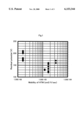
- FIG. 1 is a graph showing a relation between a residual potential of a photosensitive material and a mobility of a hole transferring material (HTM).
- HTM hole transferring material
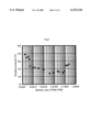
- FIG. 2 is a graph showing a relation between a residual potential of a photosensitive material and a mobility ratio [electron transferring material (ETM)/hole transferring material (HTM)] in case where a mobility of the hole transferring material at an electric field strength of 5 ⁇ 10 5 V/cm is not less than 1 ⁇ 10 -5 cm 2 /V/sec.
- ETM electron transferring material
- HTM hole transferring material
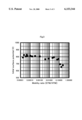
- FIG. 3 is a graph showing a relation between an initial surface potential of a photosensitive material and a mobility ratio [electron transferring material (ETM)/hole transferring material (HTM)] in case where a mobility of the hole transferring material at an electric field strength of 5 ⁇ 10 5 V/cm is not less than 1 ⁇ 10 -5 cm 2 /V/sec.
- ETM electron transferring material
- HTM hole transferring material
- the single-layer type electrophotosensitive material is that obtained by providing a single photosensitive layer on a conductive substrate.
- This photosensitive layer is formed by dissolving or dispersing an electric charge generating material, a hole transferring material, an electron transferring material and a binder resin in a proper solvent, coating the resulting coating solution on a conductive substrate, and drying the coating solution.
- the electric charge generating material includes, for example, phthalocyanine pigment, polycyclic quinone pigment, azo pigment, perylene pigment, indigo pigment, quinacridone pigment, azulenium salt pigment, squalium pigment, cyanine pigment, pyrylium dye, thiopyrylium dye, xanthene dye, quinoneimine pigment, triphenylmethane pigment, styryl pigment, selenium, tellurium, amorphous silicon, and cadmium sulfide, and these electric charge generating materials can be used alone, or two or more kinds of them can be used in combination.
- These electric charge generating materials are preferably contained in the amount within a range from 0.1 to 30% by weight, and more preferably from 0.5 to 10% by weight, based on the binder resin.
- phthalocyanine pigments such as metal-free phthalocyanine represented by the general formula (CG1) and oxotitanyl phthalocyanine represented by the general formula (CG2) are preferably used because a photosensitive material having a sensitivity within a wavelength range of not less than 700 nm is required in an image forming apparatus such as laser beam printer using a light source such as semiconductor laser, facsimile and the like.
- the crystal form of the phthalocyanine pigment is not specifically limited, and various phthalocyanine pigments can be used.
- the hole transferring material used in the photosensitive material of the present invention has a mobility of not less than 1 ⁇ 10 -5 cm 2 /V/sec at an electric field strength of 5 ⁇ 10 5 V/cm.
- the hole transferring material includes, for example, compounds represented by the following general formulas (HT-1) to (HT-3).
- these hole transferring materials can be used alone, or two or more kinds of them can be used in combination.
- the amount of the hole transferring material is preferably within a range from 5 to 500% by weight, and more preferably from 25 to 200% by weight, based on the binder resin.
- the electron transferring material used in the single-layer type positive charging photosensitive material of the present invention has a mobility of not less than 1/20000 and not more than 1/10 relative to that of the hole transferring material described above.
- the electron transferring material includes, for example, compounds represented by the following general formulas (ET-1) to (ET-7). (ET1) having a mobility of 1.75 ⁇ 10 -9 cm 2 /V/sec ##STR6##
- these electron transferring materials can be used alone or two or more kinds of them can be used in combination.
- the amount of the electron transferring material is preferably within a range from 5 to 100% by weight, and more preferably from 10 to 80% by weight, based on the binder resin.
- the mobility was measured at normal temperature by a conventional TOF (Time Of Flight) method.
- the electric field strength was 5 ⁇ 10 5 V/cm.
- the measuring sample was made by dissolving 40% by weight of an electric charge transferring material in a binder resin (bis-Z type polycarbonate resin having a weight-average molecular weight of 20,000), coating the resulting coating solution on a substrate, and subjecting to a heat treatment at 80° C. for 30 minutes.
- the film thickness of the sample is 7 ⁇ m.
- thermoplastic resins such as styrene polymer, styrene-butadiene copolymer, styrene-acrylonitrile copolymer, styrene-maleic acid copolymer, acrylic polymer, styrene-acrylic copolymer, polyethylene, ethylene-vinyl acetate copolymer, chlorinated polyethylene, polyvinyl chloride, polypropylene, ionomer, vinyl chloride-vinyl acetate copolymer, polyester, alkyd resin, polyamide, polyurethane, polycarbonate, polyacrylate, polysulfone, diallyl phthalate resin, ketone resin, polyvinyl butyral resin, and polyether resin; crosslinkable thermosetting resins such as silicone resin, epoxy resin, phenol resin,
- additives such as antioxidants, radical scavengers, singlet quenchers, deterioration inhibirtors (e.g. ultraviolet absorbers), softeners, plasticizers, surface modifiers, extenders, thickeners, dispersion stabilizers, waxes, acceptors, and donors can be incorporated into the photosensitive layer as far as the additives do not exert a deleterious influence on electrophotographic characteristics.
- known sensitizers such as terphenyl, halonaphthoquinones, and acenaphthylene may be used in combination with the electric charge generating material.
- the thickness of the photosensitive layer in the single-layer type positive charging electrophotosensitive material is within a range from 5 to 100 ⁇ , and preferably from 10 to 50 ⁇ m.
- a barrier layer may be formed between the conductive substrate and photosensitive layer as far as it does not inhibit characteristics of the photosensitive material.
- a protective layer may be formed on the surface of the photosensitive material.
- the conductive substrate on which the photosensitive layer is formed for example, various materials having the conductivity can be used.
- the conductive substrate includes, for example, metallic simple substances such as iron, aluminum, copper, tin, platinum, silver, vanadium, molybdenum, chrome, cadmium, titanium, nickel, palladium, indium, stainless steel, and brass; plastic materials prepared by depositing or laminating the above metal; and glasses coated with aluminum iodide, tin oxide, and indium oxide.
- the conductive substrate may be in the form of a sheet or drum according to the structure of the image forming apparatus to be used.
- the substrate itself may have the conductivity, or the surface of the substrate may have the conductivity.
- the conductive substrate may be preferably those having a sufficient mechanical strength on use.
- a dispersion is prepared by dispersing and mixing the above hole transferring material, electric charge generating material, electron acceptor and binder resin, together with a proper solvent, using a known method such as roll mill, ball mill, attritor, paint shaker, and ultrasonic dispersing equipment, and then the resulting dispersion is coated by using a known means and dried.
- the organic solvent includes, for example, alcohols such as methanol, ethanol, isopropanol, and butanol; aliphatic hydrocarbons such as n-hexane, octane, and cyclohexane; aromatic hydrocarbons such as benzene, toluene, and xylene; halogenated hydrocarbons such as dichloromethane, dichloroethane, chloroform, carbon tetrachloride, and chlorobenzene; ethers such as dimethyl ether, diethyl ether, tetrahydrofuran, ethylene glycol dimethyl ether, and diethylene glycol dimethyl ether; ketones such as acetone, methyl ethyl ketone, and cylohexanone; esters such as ethyl acetate and methyl acetate; and dimethylformaldehyde, dimethyl
- surfactants and leveling agents may be used.
- a X type metal-free phthalocyanine (CGM) as the electric charge generating material 65 parts by weight of a hole transferring material [one selected from (HT1) to (HT3)], 30 parts by weight of an electron transferring material [one selected from (ET1) to (ET7)], 100 parts by weight of a bisphenol Z type polycarbonate resin having a weight-average molecular weight of 30,000 as the binder resin, and 760 parts by weight of tetrahydrofuran were mixed and dispersed in a ball mill for 27 hours to prepare a coating solution for single-layer type photosensitive layer. Then, this coating solution was coated on an aluminum tube as the conductive substrate by using the dip coating method, followed by hot-air drying at 110° C. for 40 minutes to obtain a single-layer type photosensitive material having a single photosensitive layer of 27.5 ⁇ m in film thickness, respectively.
- CGM X type metal-free phthalocyanine
- the residual potential must be 170 V or less.
- the initial surface potential must be 750 V or more.
- Each of the electrophotosensitive materials obtained in the respective Examples and Comparative Examples was mounted to a high-speed image forming apparatus capable of taking 50 or more copies of a A4-size original per minute [Creage 7350, manufactured by Mita Industries Co., Ltd.] and a practical copying test was effected. Then, a solid reflection density was measured by using a reflection densitometer manufactured by Nippon Denshoku Co., Ltd.
- An image density (ID) is a value obtained by measuring the density of the solid black portion.
- a fog density (FD) is a density obtained by subtracting a reflection density of a white paper before copying from a reflection density of the non-image area after copying.
- the image density of not less than 1.3 was rated "pass", while the image density of smaller than 1.3 was rated “fail”.
- the fog density of not more than 0.005 was rated "pass”, while the fog density of not less than 0.006 was rated "fail”.
- V residual potential
- ETM electron transferring material
- HTM hole transferring material
- the residual potential V L of the photosensitive material is not more than 170 V and the initial surface potential V 0 is not less than 750 V in case where the mobility ratio is not less than 1/20000 and not more than 1/10.
- image fog did not occur even in a practical test using a high-speed image forming apparatus capable of taking 50 or more copies of a A4-size original and a sufficient image density having ID of not less than 1.3 was obtained.
Landscapes
- Physics & Mathematics (AREA)
- General Physics & Mathematics (AREA)
- Photoreceptors In Electrophotography (AREA)
Abstract
The present invention relates to a positive charging single-layer type electrophotosensitive material comprising a conductive substrate and a photosensitive layer provided on the conductive substrate, said photosensitive layer comprising an electron charge generating material, a hole transferring material, an electron transferring material and a binder resin, wherein a mobility of the hole transferring material at an electric field strength of 5×10⁵ V/cm is not less than 1×10⁻⁵ cm2 /V/sec and the electron transferring material has a mobility of not less than 1/20000 and not more than 1/10 relative to that of the hole transferring material. Said positive charging single-layer type photosensitive material has a sufficient sensitivity even when used in a high-speed image forming apparatus capable of taking 50 or more copies of a A4-size original.
Description
1. Field of the Invention
The present invention relates to an electrophotosensitive material which is used in image forming apparatuses such as electrostatic copying machine, facsimile, laser beam printer and the like.
2. Description of the Prior Art
In the image forming apparatuses, various organic photosensitive materials having a sensitivity within a wavelength range of a light source used in the image forming apparatuses can be used. Recently, these organic photosensitive materials have widely been used because of easier production than that in the case of a conventional inorganic photosensitive material, various selective materials for photosensitive material, for example, electric charge transferring material, electric charge generating material, binding resin, etc., and high design freedom.
The organic photosensitive material includes, for example, a single-layer type photosensitive material wherein an electric charge transferring material and an electric charge generating material are dispersed in the same photosensitive layer, and a multi-layer photosensitive meterial comprising an electric charge generating layer containing an electric charge generating material and an electron transferring layer containing an electron transferring material, which are mutually laminated.
The single-layer type photosensitive material has attracted special interest recently by the following reasons. That is, the single-layer type photosensitive material can be easily produced because of its simple structure and film defects can be inhibited on formation of layers and, furthermore, optical characteristics can be improved because of less interface between layers. The single-layer type photosensitive material can be used in any of positive and negative charging type apparatuses, but is exclusively used in a positive charging type apparatus in view of characteristics of constituent materials of the photosensitive material.
An image forming apparatus using the single-layer type photosensitive material has the following advantages and a market for the image forming apparatus has been cultivated.
(1) High image quality is attained because turbulance of move of electric charges between the electric charge generating layer and electric charge transferring layer occurs, like a multi-layer type one.
(2) When using in a positive charging type pparatus, ozone which is detrimental to the human body is hardly evolved.
To meet requirements to an image forming apparatus, such as high speed and energy saving, which have recently been increased more and more, the sensitivity of a conventional single-layer photosensitive material has become insufficient at present.
When using a conventional positive charging single-layer type electrophotosensitive material in an image forming apparatus having a high process speed, which is capable of taking 50 or more copies of a A4-size original, a dose of exposure light is small and a time required for a photosensitive material drum to move from the exposure position to the developing position is short, thereby causing a phenomenon that a developing process is attained during potential attenuation due to exposure.
As a result, the following problems occur. That is, an excess dose of light is required to lower a light potential of the photosensitive material and a change in light potential due to an environmental change increases because of the potential attenuation and, furthermore, the degree of fatigue in the photosensitive material due to repeating of exposure and development becomes severe. Consequently, it becomes difficult to obtain a good image.
Thus, an object of the present invention is to provide a positive charging single-layer type electrophotosensitive material, which has particularly high sensitivity and can sufficiently meet requirements to an image forming apparatus, such as high speed and energy saving.
To solve the above problems, the present inventors have intensively studied and found that there can be obtained a positive charging single-layer type photosensitive material comprising at least an electron charge generating material, a hole transferring material, an electron transferring material and a binder resin, which has a sufficient sensitivity even when used in a high-speed image forming apparatus capable of taking 50 or more copies of a A4-size original, in case where a mobility of the hole transferring material at an electric field strength of 5×10⁵ V/cm is not less than 1×10⁻⁵ cm2 /V/sec and the electron transferring material has a mobility of not less than 1/20000 and not more than 1/10 relative to that of the hole transferring material. Thus, the present invention has been completed and includes the following inventions:
(1) A positive charging single-layer type electrophotosensitive material comprising a conductive substrate and a photosensitive layer provided on the conductive substrate, said photosensitive layer comprising an electron charge generating material, a hole transferring material, an electron transferring material and a binder resin, wherein a mobility of the hole transferring material at an electric field strength of 5×10⁵ V/cm is not less than 1×10⁻⁵ cm2 /V/sec and the electron transferring material has a mobility of not less than 1/20000 and not more than 1/10 relative to that of the hole transferring material.
(2) The positive charging single-layer type electrophotosensitive material according to the item 1, wherein the electric charge generating material is a phthalocyanine compound.
(3) The positive charging single-layer type electrophotosensitive material according to the item 2, wherein a residual potential at the time of irradiation with monochromic light having a wavelength of 780 nm and a light intensity of 15 μW for 40 msec is not more than 170 V.
(4) The positive charging single-layer type electrophotosensitive material according to the item 2, herein an initial surface potential at the time at which a value of a current to be applied into the photosensitive layer is 12 μA is not less than 750 V.
(5) A high-speed digital image forming apparatus, which is capable of taking 50 or more copies of a A4-size original wherein the positive charging single-layer type electrophotosensitive material of the item 2 is used in said apparatus.
According to the present invention, there can be obtained a positive charging single-layer type photosensitive material comprising at least an electron charge generating material, a hole transferring material, an electron transferring material and a binder resin, which has a sufficient sensitivity even when used in a high-speed image forming apparatus capable of taking 50 or more copies of a A4-size original, in case where a mobility of the hole transferring material at an electric field strength of 5×10⁵ V/cm is not less than 1×10⁻⁵ cm2 /V/sec and the electron transferring material has a mobility of not less than 1/20000 and not more than 1/10 relative to that of the hole transferring material.
The reason why the positive charging single-layer type photosensitive material having a high sensitivity could be obtained as described above is assumed as follows.
Among photoproduced carriers, electrons reach the surface of a photosensitive layer, whereas, holes reach a conductive substrate side, thereby to cause photoattenuation. Since the generation of electric charges is unevenly distributed in the vicinity of the surface of the photosensitive layer, the mobility of holes are longer than that of electrons, necessarily.
First, when the mobility of an electron transferring material is smaller than 1/20000 as compared with a hole transferring material having a mobility of not less than 1×10⁻⁵ cm2 /V/sec at an electric field strength of 5×10⁵ V/cm, electrons which could not reach the surface of the photosensitive layer are remained in the photosensitive layer due to a difference in mobility between the hole transferring material and electron transferring material. Therefore, the electric charge generation efficiency does not increase, which leads to lowering of the sensitivity of the photosensitive material, thereby making it difficult to obtain a sufficient image density in a high-speed image forming apparatus.
On the other hand, when the mobility of the electron transferring material is 1/10 times larger than that of the hole transferring material, positive electric charges on the surface of the photosensitive layer are negated before holes reach the conductive substrate, thereby to lower the electric field strength of the photosensitive layer. Therefore, the mobility of holes is controlled furthermore, thereby to lower the sensitivity. Since positive electric charges of the surface of the photosensitive layer are negated, the surface potential of the photosensitive material tends to be lowered and image fog is liable to occur.
FIG. 1 is a graph showing a relation between a residual potential of a photosensitive material and a mobility of a hole transferring material (HTM).
FIG. 2 is a graph showing a relation between a residual potential of a photosensitive material and a mobility ratio [electron transferring material (ETM)/hole transferring material (HTM)] in case where a mobility of the hole transferring material at an electric field strength of 5×10⁵ V/cm is not less than 1×10⁻⁵ cm2 /V/sec.
FIG. 3 is a graph showing a relation between an initial surface potential of a photosensitive material and a mobility ratio [electron transferring material (ETM)/hole transferring material (HTM)] in case where a mobility of the hole transferring material at an electric field strength of 5×10⁵ V/cm is not less than 1×10⁻⁵ cm2 /V/sec.
The single-layer type electrophotosensitive material is that obtained by providing a single photosensitive layer on a conductive substrate. This photosensitive layer is formed by dissolving or dispersing an electric charge generating material, a hole transferring material, an electron transferring material and a binder resin in a proper solvent, coating the resulting coating solution on a conductive substrate, and drying the coating solution.
Various materials used in the positive charging single-layer type electrophotosensitive material of the present invention will be described below.
<Electric charge generating agent>
The electric charge generating material includes, for example, phthalocyanine pigment, polycyclic quinone pigment, azo pigment, perylene pigment, indigo pigment, quinacridone pigment, azulenium salt pigment, squalium pigment, cyanine pigment, pyrylium dye, thiopyrylium dye, xanthene dye, quinoneimine pigment, triphenylmethane pigment, styryl pigment, selenium, tellurium, amorphous silicon, and cadmium sulfide, and these electric charge generating materials can be used alone, or two or more kinds of them can be used in combination. These electric charge generating materials are preferably contained in the amount within a range from 0.1 to 30% by weight, and more preferably from 0.5 to 10% by weight, based on the binder resin. Among these electric charge generating material, for example, phthalocyanine pigments such as metal-free phthalocyanine represented by the general formula (CG1) and oxotitanyl phthalocyanine represented by the general formula (CG2) are preferably used because a photosensitive material having a sensitivity within a wavelength range of not less than 700 nm is required in an image forming apparatus such as laser beam printer using a light source such as semiconductor laser, facsimile and the like. The crystal form of the phthalocyanine pigment is not specifically limited, and various phthalocyanine pigments can be used.
(CG1) Metal-free phthalocyanine ##STR1##
(CG2) Oxotitanyl phthalocyanine ##STR2## <Hole transferring material>
It is necessary that the hole transferring material used in the photosensitive material of the present invention has a mobility of not less than 1×10⁻⁵ cm2 /V/sec at an electric field strength of 5×10⁵ V/cm. The hole transferring material includes, for example, compounds represented by the following general formulas (HT-1) to (HT-3).
(HT1) having a mobility of 1.21×10⁻⁵ cm2 /V/sec ##STR3##
(HT2) having a mobility of 1.69×10⁻⁵ cm2 /V/sec ##STR4##
(HT3) having a mobility of 3.83×10⁻⁵ cm2 /V/sec ##STR5##
In the present invention, these hole transferring materials can be used alone, or two or more kinds of them can be used in combination. The amount of the hole transferring material is preferably within a range from 5 to 500% by weight, and more preferably from 25 to 200% by weight, based on the binder resin.
<Electron transferring material>
It is necessary that the electron transferring material used in the single-layer type positive charging photosensitive material of the present invention has a mobility of not less than 1/20000 and not more than 1/10 relative to that of the hole transferring material described above. The electron transferring material includes, for example, compounds represented by the following general formulas (ET-1) to (ET-7). (ET1) having a mobility of 1.75×10⁻⁹ cm2 /V/sec ##STR6##
(ET2) having a mobility of 5.32×10⁻⁹ cm2 /V/sec ##STR7##
(ET3) having a mobility of 1.67×10⁻⁸ cm2 /V/sec ##STR8##
(ET4) having a mobility of 6.13×10⁻⁸ cm2 /V/sec ##STR9##
(ET5) having a mobility of 1.37×10⁻⁷ cm2 /V/sec ##STR10##
(ET6) having a mobility of 3.47×10⁻⁷ cm2 /V/sec ##STR11##
(ET7) having a mobility of 1.04×10⁻⁶ cm2 /V/sec ##STR12##
In the present invention, these electron transferring materials can be used alone or two or more kinds of them can be used in combination. The amount of the electron transferring material is preferably within a range from 5 to 100% by weight, and more preferably from 10 to 80% by weight, based on the binder resin.
The mobility was measured at normal temperature by a conventional TOF (Time Of Flight) method. The electric field strength was 5×10⁵ V/cm. The measuring sample was made by dissolving 40% by weight of an electric charge transferring material in a binder resin (bis-Z type polycarbonate resin having a weight-average molecular weight of 20,000), coating the resulting coating solution on a substrate, and subjecting to a heat treatment at 80° C. for 30 minutes. The film thickness of the sample is 7 μm.
<Binder resin>
As the binder resin in which the above respective components are dispersed, there can be used various resins which have hitherto been used in the photosensitive layer. For example, there can be used thermoplastic resins such as styrene polymer, styrene-butadiene copolymer, styrene-acrylonitrile copolymer, styrene-maleic acid copolymer, acrylic polymer, styrene-acrylic copolymer, polyethylene, ethylene-vinyl acetate copolymer, chlorinated polyethylene, polyvinyl chloride, polypropylene, ionomer, vinyl chloride-vinyl acetate copolymer, polyester, alkyd resin, polyamide, polyurethane, polycarbonate, polyacrylate, polysulfone, diallyl phthalate resin, ketone resin, polyvinyl butyral resin, and polyether resin; crosslinkable thermosetting resins such as silicone resin, epoxy resin, phenol resin, urea resin, and melamine resin; and photocurable resins such as epoxy acrylate and urethane acrylate. These binder resins can be used alone, or two or more kinds of them can be used in combination.
In addition to the above respective components, various conventionally known additives such as antioxidants, radical scavengers, singlet quenchers, deterioration inhibirtors (e.g. ultraviolet absorbers), softeners, plasticizers, surface modifiers, extenders, thickeners, dispersion stabilizers, waxes, acceptors, and donors can be incorporated into the photosensitive layer as far as the additives do not exert a deleterious influence on electrophotographic characteristics. To improve the sensitivity of the photosensitive layer, for example, known sensitizers such as terphenyl, halonaphthoquinones, and acenaphthylene may be used in combination with the electric charge generating material.
The thickness of the photosensitive layer in the single-layer type positive charging electrophotosensitive material is within a range from 5 to 100μ, and preferably from 10 to 50 μm.
In the single-layer type positive charging electrophotosensitive material, a barrier layer may be formed between the conductive substrate and photosensitive layer as far as it does not inhibit characteristics of the photosensitive material. A protective layer may be formed on the surface of the photosensitive material.
As the conductive substrate on which the photosensitive layer is formed, for example, various materials having the conductivity can be used. The conductive substrate includes, for example, metallic simple substances such as iron, aluminum, copper, tin, platinum, silver, vanadium, molybdenum, chrome, cadmium, titanium, nickel, palladium, indium, stainless steel, and brass; plastic materials prepared by depositing or laminating the above metal; and glasses coated with aluminum iodide, tin oxide, and indium oxide.
The conductive substrate may be in the form of a sheet or drum according to the structure of the image forming apparatus to be used. The substrate itself may have the conductivity, or the surface of the substrate may have the conductivity. The conductive substrate may be preferably those having a sufficient mechanical strength on use.
When the photosensitive layer is formed by the coating method, a dispersion is prepared by dispersing and mixing the above hole transferring material, electric charge generating material, electron acceptor and binder resin, together with a proper solvent, using a known method such as roll mill, ball mill, attritor, paint shaker, and ultrasonic dispersing equipment, and then the resulting dispersion is coated by using a known means and dried.
As the solvent for preparing the dispersion, various organic solvents can be used. The organic solvent includes, for example, alcohols such as methanol, ethanol, isopropanol, and butanol; aliphatic hydrocarbons such as n-hexane, octane, and cyclohexane; aromatic hydrocarbons such as benzene, toluene, and xylene; halogenated hydrocarbons such as dichloromethane, dichloroethane, chloroform, carbon tetrachloride, and chlorobenzene; ethers such as dimethyl ether, diethyl ether, tetrahydrofuran, ethylene glycol dimethyl ether, and diethylene glycol dimethyl ether; ketones such as acetone, methyl ethyl ketone, and cylohexanone; esters such as ethyl acetate and methyl acetate; and dimethylformaldehyde, dimethylformamide, and dimethyl sulfoxide. These solvents can be used alone, or two or more kinds of them can be used in combination.
To improve the dispersion properties of the electric charge generating material, hole transferring material and electron transferring material, and the smoothness of the surface of the photosensitive layer, for example, surfactants and leveling agents may be used.
<Examples>
The following Examples and Comparative Examples further illustrate the present invention. The following embodiments are therefore to be considered as illustrative and the technical scope of the present invention is not limited by the embodiments.
4.5 Parts by weight of a X type metal-free phthalocyanine (CGM) as the electric charge generating material, 65 parts by weight of a hole transferring material [one selected from (HT1) to (HT3)], 30 parts by weight of an electron transferring material [one selected from (ET1) to (ET7)], 100 parts by weight of a bisphenol Z type polycarbonate resin having a weight-average molecular weight of 30,000 as the binder resin, and 760 parts by weight of tetrahydrofuran were mixed and dispersed in a ball mill for 27 hours to prepare a coating solution for single-layer type photosensitive layer. Then, this coating solution was coated on an aluminum tube as the conductive substrate by using the dip coating method, followed by hot-air drying at 110° C. for 40 minutes to obtain a single-layer type photosensitive material having a single photosensitive layer of 27.5 μm in film thickness, respectively.
In the same manner as in Examples 1 to 11, except for using one selected from (ET8) to (ET1) as the electron transferring material, single-layer type photosensitive materials were produced, respectively. (ET8) having a mobility of 6.00×10⁻¹⁰ cm2 /V/sec ##STR13##
(ET9) having a mobility of 7.56×10⁻¹⁰ cm2 /V/sec ##STR14##
(ET10) having a mobility of 2.08×10⁻⁶ cm2 /V/sec ##STR15##
(ET11) having a mobility of 2.77×10⁻⁶ cm2 /V/sec ##STR16##
In the same manner as in Examples 1 to 11, except for using (HT4) as the hole transferring material, single-layer type photosensitive materials were produced, respectively. (HT4) having a mobility of 1.60×10⁻⁶ cm2 /V/sec ##STR17##
The electrophotosensitive materials of the above respective Examples and Comparative Examples were subjected to the following test and the characteristics were evaluated, respectively.
<Evaluation of initial sensitivity>
Using a drum sensitivity tester (trade name: GENETEC SINCIA 30M) manufactured by GENETEC Co., a voltage was applied on the surface of each of electrophotosensitive materials of the respective Examples and Comparative Examples to charge the surface at +800 V.
Then, monochromic light having a wavelength of 780 nm (half-width: 20 nm, light intensity: 15 μW/cm2) from white light of a halogen lamp as an exposure light source of the above tester through a band-pass filter was irradiated on the surface of each of electrophotosensitive materials in the charged state (exposure time: 40 msec). Furthermore, a surface potential at the time at which 500 msec have passed since the beginning of exposure was measured as a residual potential VL (V). The smaller the residual potential, the higher the sensitivity of the photosensitive material.
To obtain a sufficient image density in a high-speed image forming apparatus capable of taking 50 or more copies of a A4-size original per minute, the residual potential must be 170 V or less.
<Evaluation of initial charging>
Using the above drum sensitivity tester, an initial surface potential V0 (V) of each of electrophotosensitive materials of the respective Examples and Comparative Examples was measured at a value of a current to be applied of 12 μA. Charging was effected by a corotron system.
To obtain an image, which is free from fog, in a high-speed image forming apparatus capable of taking 50 or more copies of a A4-size original per minute, the initial surface potential must be 750 V or more.
<Evaluation of image>
Each of the electrophotosensitive materials obtained in the respective Examples and Comparative Examples was mounted to a high-speed image forming apparatus capable of taking 50 or more copies of a A4-size original per minute [Creage 7350, manufactured by Mita Industries Co., Ltd.] and a practical copying test was effected. Then, a solid reflection density was measured by using a reflection densitometer manufactured by Nippon Denshoku Co., Ltd.
An image density (ID) is a value obtained by measuring the density of the solid black portion. A fog density (FD) is a density obtained by subtracting a reflection density of a white paper before copying from a reflection density of the non-image area after copying.
The image density of not less than 1.3 was rated "pass", while the image density of smaller than 1.3 was rated "fail". The fog density of not more than 0.005 was rated "pass", while the fog density of not less than 0.006 was rated "fail".
The evaluation results are shown in Table 1. In case where the mobility of the hole transferring material at the electric field strength of 5×10⁵ V/cm is smaller than 1×10⁻⁵ cm2 /V/sec (shown in Comparative Examples 8 to 14), the residual potential VL of the photosensitive material became larger than 170 V and a sufficient image density could not be obtained, as shown in FIG. 1.
A relation between a residual potential VL (V) and a mobility ratio [electron transferring material (ETM)/hole transferring material (HTM)] in case where a mobility of the hole transferring material at an electric field strength of 5×10⁵ V/cm is not less than 1×10⁻⁵ cm2 /V/sec is shown in FIG. 2, while a relation between an initial surface potential V0 and a mobility ratio is shown in FIG. 3 (with respect to Examples 1 to 11 and Comparative Examples 1 to 7).
As is apparent from FIGS. 2 and 3, the residual potential VL of the photosensitive material is not more than 170 V and the initial surface potential V0 is not less than 750 V in case where the mobility ratio is not less than 1/20000 and not more than 1/10. As is apparent from Table 1, image fog did not occur even in a practical test using a high-speed image forming apparatus capable of taking 50 or more copies of a A4-size original and a sufficient image density having ID of not less than 1.3 was obtained.
On the other hand, in case where the mobility ratio is smaller than 1/20000, the residual potential VL of the photosensitive material became larger than 170 V and a sufficient image density could not be obtained. In case where the mobility ratio is larger than 1/10, the initial surface potential V0 of the photosensitive material was smaller than 750 V and image fog occurred.
                                  TABLE 1
__________________________________________________________________________
                   Mobility     Mobility
  Examples/Comp. Examples Kind of HTM [cm.sup.2 /V/sec] Kind of ETM
                                [cm.sup.2 /V/sec]
__________________________________________________________________________
Example 1   HT1    1.21 × 10.sup.-5
                         ET7    1.04 × 10.sup.-6
  Example 2 HT2 1.69 × 10.sup.-5 ET7 1.04 × 10.sup.-6
                                 Example 3 HT1 1.21 × 10.sup.-5 ET6
                                3.47 × 10.sup.-7
  Example 4 HT2 1.69 × 10.sup.-5 ET6 3.47 × 10.sup.-7
                                 Example 5 HT2 1.69 × 10.sup.-5 ET5
                                1.37 × 10.sup.-7
  Example 6 HT2 1.69 × 10.sup.-5 ET4 6.13 × 10.sup.-8
                                 Example 7 HT2 1.59 × 10.sup.-5 ET3
                                1.67 × 10.sup.-8
  Example 8 HT2 1.69 × 10.sup.-5 ET2 5.32 × 10.sup.-9
                                 Example 9 HT3 3.38 × 10.sup.-5 ET2
                                5.32 × 10.sup.-9
  Example 10 HT2 1.69 × 10.sup.-5 ET1 1.75 × 10.sup.-9
                                 Example 11 HT3 3.38 × 10.sup.-5
                                ET1 1.75 × 10.sup.-9
  Comp. Example 1 HT2 1.69 × 10.sup.-5  ET10 2.08 × 10.sup.-6
  Comp. Example 2 HT2 1.69 × 10.sup.-5  ET11 2.77 × 10.sup.-6
  Comp. Example 3 HT1 1.21 × 10.sup.-5  ET11 2.77 × 10.sup.-6
  Comp. Example 4 HT2 1.69 × 10.sup.-5 ET9  7.56 × 10.sup.-10
  Comp. Example 5 HT2 1.69 × 10.sup.-5 ET8  6.00 × 10.sup.-10
  Comp. Example 6 HT3 3.38 × 10.sup.-5 ET9  7.56 × 10.sup.-10
  Comp. Example 7 HT3 3.38 × 10.sup.-5 ET8  6.00 × 10.sup.-10
  Comp. Example 8 HT4 1.60 × 10.sup.-6 ET7 1.04 × 10.sup.-6
                                 Comp. Example 9 HT4 1.60 ×
                                10.sup.-6 ET6 3.47 × 10.sup.-7
                                 Comp. Example 10 HT4 1.60 ×
                                10.sup.-6 ET5 1.37 × 10.sup.-7
                                 Comp. Example 11 HT4 1.60 ×
                                10.sup.-6 ET4 6.13 × 10.sup.-8
                                 Comp. Example 12 HT4 1.60 ×
                                10.sup.-6 ET3 1.67 × 10.sup.-8
                                 Comp. Example 13 HT4 1.60 ×
                                10.sup.-6 ET2 5.32 × 10.sup.-9
                                 Comp. Example 14 HT4 1.60 ×
                                10.sup.-6 ET1 1.75 × 10.sup.-9
__________________________________________________________________________
            Mobility
                  Residual
                       Surface
                            Image
   ratio potential potential density Fog density
  Examples/Comp. Examples (ETM/HTM) V
                                 .sub.L [V] V.sub.O [V] ID FD
__________________________________________________________________________
Example 1   0.085950
                  132  770  1.37 0.003
  Example 2 0.061538 125 760 1.37 0.003
  Example 3 0.028678 130 795 1.38 0.004
  Example 4 0.020533 135 785 1.38 0.002
  Example 5 0.008107 125 775 1.37 0.003
  Example 6 0.003627 120 765 1.37 0.004
  Example 7 0.000988 145 805 1.36 0.004
  Example 8 0.000315 155 810 1.34 0.004
  Example 9 0.000157 160 805 1.37 0.002
  Example 10 0.000104 160 815 1.36 0.003
  Example 11 0.000052 170 810 1.31 0.004
  Comp. Example 1 0.123077 171 695 1.28 0.011
  Comp. Example 2 0.163905 172 655 1.27 0.016
  Comp. Example 3 0.228926 180 680 1.23 0.014
  Comp. Example 4 0.000045 215 830 1.21 0.004
  Comp. Example 5 0.000038 230 805 1.22 0.005
  Comp. Example 6 0.000022 225 825 1.21 0.004
  Comp. Example 7 0.000018 245 790 1.23 0.005
  Comp. Example 8 0.650000 180 780 1.21 0.003
  Comp. Example 9 0.216875 179 780 1.19 0.003
  Comp. Example 10 0.085625 174 770 1.21 0.003
  Comp. Example 11 0.038313 175 760 1.24 0.004
  Comp. Example 12 0.010438 200 800 1.26 0.004
  Comp. Example 13 0.003325 205 805 1.18 0.004
  Comp. Example 14 0.001094 210 810 1.17 0.005
__________________________________________________________________________
The disclosure of Japanese Patent Application Serial No.11-141646, filed on May 21, 1999, is incorporated herein by reference.
Claims (5)
1. A positive charging single-layer type electrophotosensitive material comprising a conductive substrate and a photosensitive layer provided on the conductive substrate, said photosensitive layer comprising an electron charge generating material, a hole transferring material, an electron transferring material and a binder resin, characterized in that a mobility of the hole transferring material at an electric field strength of 5×10⁵ V/cm is not less than 1×10⁻⁵ cm2 /V/sec and that the electron transferring material has a mobility of not less than 1/20000 and not more than 1/10 relative to that of the hole transferring material.
2. The positive charging single-layer type electrophotosensitive material according to claim 1, wherein the electric charge generating material is a phthalocyanine compound.
3. The positive charging single-layer type electrophotosensitive material according to claim 2, wherein a residual potential at the time of irradiation with monochromic light having a wavelength of 780 nm and a light intensity of 15 μW for 40 msec is not more than 170 V.
4. The positive charging single-layer type electrophotosensitive material according to claim 2, wherein an initial surface potential at the time at which a value of a current to be applied into the photosensitive layer is 12 μA is not less than 750 V.
5. A high-speed digital image forming apparatus, which is capable of taking 50 or more copies of a A4-size original wherein the positive charging single-layer type electrophotosensitive material of claim 2 is used in said apparatus.
Applications Claiming Priority (2)
| Application Number | Priority Date | Filing Date | Title |
|---|---|---|---|
| JP11-141646 | 1999-05-21 | ||
| JP11141646A JP2000330302A (en) | 1999-05-21 | 1999-05-21 | Positively charged monolayer type electrophotographic photoreceptor |
Publications (1)
| Publication Number | Publication Date |
|---|---|
| US6153344A true US6153344A (en) | 2000-11-28 |
Family
ID=15296896
Family Applications (1)
| Application Number | Title | Priority Date | Filing Date |
|---|---|---|---|
| US09/556,942 Expired - Lifetime US6153344A (en) | 1999-05-21 | 2000-04-21 | Positive charging single-layer type electrophotosensitive material |
Country Status (3)
| Country | Link |
|---|---|
| US (1) | US6153344A (en) |
| EP (1) | EP1054298A1 (en) |
| JP (1) | JP2000330302A (en) |
Cited By (5)
| Publication number | Priority date | Publication date | Assignee | Title |
|---|---|---|---|---|
| US20030194626A1 (en) * | 2002-04-12 | 2003-10-16 | Jiayi Zhu | Organophotoreceptor with an electron transport layer |
| US20030211413A1 (en) * | 2002-05-10 | 2003-11-13 | Xerox Corporation. | Imaging members |
| US20050089789A1 (en) * | 2002-05-31 | 2005-04-28 | Samsung Electronics Co., Ltd. | Organophotoreceptor with a light stabilizer |
| US20140120464A1 (en) * | 2012-10-31 | 2014-05-01 | Kyocera Document Solutions Inc. | Electrophotographic photosensitive member and image forming apparatus including electrophotographic photosensitive member |
| CN107193191A (en) * | 2017-06-21 | 2017-09-22 | 苏州恒久光电科技股份有限公司 | Electropositive colour organic photoconductor coating method and its obtained organic photoconductor |
Families Citing this family (3)
| Publication number | Priority date | Publication date | Assignee | Title |
|---|---|---|---|---|
| US6461779B1 (en) | 2000-11-14 | 2002-10-08 | Kyocera Mita Corporation | Single-layer type electrophotosensitive material |
| DE60121724T2 (en) * | 2001-03-19 | 2007-08-02 | Kyocera Mita Corp. | Single-layer type electrophotographic material |
| CN101713933B (en) * | 2008-10-08 | 2013-01-02 | 京瓷办公信息系统株式会社 | A mono-layer electronic photographic photoreceptor with positive electricity and an image forming apparatus |
Citations (4)
| Publication number | Priority date | Publication date | Assignee | Title |
|---|---|---|---|---|
| US5240802A (en) * | 1991-12-31 | 1993-08-31 | Eastman Kodak Company | Aggregate photoconductive element and method of making same |
| US5492784A (en) * | 1992-08-07 | 1996-02-20 | Ricoh Company, Ltd. | Positively-chargeable single-layered type electrophotographic photoconductor |
| US5968697A (en) * | 1997-02-27 | 1999-10-19 | Fuji Electric Co., Ltd. | Electrophotographic photoconductor |
| US5989766A (en) * | 1997-06-09 | 1999-11-23 | Samsung Display Devices Co., Ltd. | Photoconductive composition and display adopting photoconductive layer made thereof |
Family Cites Families (4)
| Publication number | Priority date | Publication date | Assignee | Title |
|---|---|---|---|---|
| US5324610A (en) * | 1991-03-26 | 1994-06-28 | Mita Industrial Co., Ltd. | Electrophotographic organic photosensitive material with diphenoquinone derivative |
| JPH05150491A (en) * | 1991-11-29 | 1993-06-18 | Mita Ind Co Ltd | Electrophotographic sensitive body |
| JPH07325413A (en) * | 1994-05-31 | 1995-12-12 | Mita Ind Co Ltd | Electrophotographic photoreceptor |
| US5616441A (en) * | 1994-09-20 | 1997-04-01 | Mita Industrial Co., Ltd. | Tryptoanthorine derivative contained in electrophotosensitive material |
-
1999
- 1999-05-21 JP JP11141646A patent/JP2000330302A/en active Pending
-
2000
- 2000-04-21 US US09/556,942 patent/US6153344A/en not_active Expired - Lifetime
- 2000-05-17 EP EP00304172A patent/EP1054298A1/en not_active Withdrawn
Patent Citations (4)
| Publication number | Priority date | Publication date | Assignee | Title |
|---|---|---|---|---|
| US5240802A (en) * | 1991-12-31 | 1993-08-31 | Eastman Kodak Company | Aggregate photoconductive element and method of making same |
| US5492784A (en) * | 1992-08-07 | 1996-02-20 | Ricoh Company, Ltd. | Positively-chargeable single-layered type electrophotographic photoconductor |
| US5968697A (en) * | 1997-02-27 | 1999-10-19 | Fuji Electric Co., Ltd. | Electrophotographic photoconductor |
| US5989766A (en) * | 1997-06-09 | 1999-11-23 | Samsung Display Devices Co., Ltd. | Photoconductive composition and display adopting photoconductive layer made thereof |
Cited By (7)
| Publication number | Priority date | Publication date | Assignee | Title |
|---|---|---|---|---|
| US20030194626A1 (en) * | 2002-04-12 | 2003-10-16 | Jiayi Zhu | Organophotoreceptor with an electron transport layer |
| US6890693B2 (en) | 2002-04-12 | 2005-05-10 | Samsung Electronics Co., Ltd. | Organophotoreceptor with an electron transport layer |
| US20030211413A1 (en) * | 2002-05-10 | 2003-11-13 | Xerox Corporation. | Imaging members |
| US20050089789A1 (en) * | 2002-05-31 | 2005-04-28 | Samsung Electronics Co., Ltd. | Organophotoreceptor with a light stabilizer |
| US20140120464A1 (en) * | 2012-10-31 | 2014-05-01 | Kyocera Document Solutions Inc. | Electrophotographic photosensitive member and image forming apparatus including electrophotographic photosensitive member |
| US9158264B2 (en) * | 2012-10-31 | 2015-10-13 | Kyocera Document Solutions Inc. | Electrophotographic photosensitive member and image forming apparatus including electrophotographic photosensitive member |
| CN107193191A (en) * | 2017-06-21 | 2017-09-22 | 苏州恒久光电科技股份有限公司 | Electropositive colour organic photoconductor coating method and its obtained organic photoconductor |
Also Published As
| Publication number | Publication date |
|---|---|
| JP2000330302A (en) | 2000-11-30 |
| EP1054298A1 (en) | 2000-11-22 |
Similar Documents
| Publication | Publication Date | Title |
|---|---|---|
| JPH10237347A (en) | Crystalline oxotitanyl phthalocyanine and electrophotographic photoreceptor using the same, and image formation using the same | |
| US5506082A (en) | Cross-linked polyvinyl butyral binder for organic photoconductor | |
| US6153344A (en) | Positive charging single-layer type electrophotosensitive material | |
| JP4898411B2 (en) | Image forming member | |
| EP1198735B1 (en) | Electrophotographic photoconductor containing simple quinones to improve electrical properties | |
| CN104281021A (en) | Electrophotographic photoreceptor and image forming apparatus including the same | |
| JP2008139372A (en) | Laminate type electrophotographic photoreceptor and image forming device | |
| US5952139A (en) | Electrophotographic photoconductor | |
| JP3876958B2 (en) | Electrophotographic photosensitive member, manufacturing method thereof, and electrophotographic apparatus | |
| JP3066882B2 (en) | Electrophotographic photoreceptor | |
| US4891288A (en) | Photoreceptor for positive electrostatic charge | |
| JP4020648B2 (en) | Image forming method using positively charged single layer type electrophotographic photosensitive member | |
| JP5718413B2 (en) | Electrophotographic photosensitive member and image forming apparatus using the same | |
| US5376487A (en) | Photosensitive member containing specified arylamine compound and electron-accepting compound | |
| DE102015106165A1 (en) | ELECTROPHOTOGRAPHIC PHOTOSENSITIVE ELEMENT, METHOD FOR PRODUCING AN ELECTROPHOTOGRAPHIC PHOTOSENSITIVE ELEMENT, PROCESS CARTRIDGE AND ELECTROPHOTOGRAPHIC APPARATUS, AND HYDROXYGALLIUM PHTHALOCYANINE CRYSTALL | |
| JP2006065353A (en) | Single-layer electrophotographic photoreceptor and method for manufacturing the same | |
| JP7180175B2 (en) | Image forming apparatus and image forming method | |
| JPH07175233A (en) | Single layer type electrophotographic photoreceptor | |
| JP3489187B2 (en) | Electrophotographic photoreceptor | |
| JP2002221806A (en) | Image forming method using positively chargeable monolayer electrophotographic photoreceptor | |
| JP2002258502A (en) | Image forming method using positive-charged single layer electrophotographic sensitive body | |
| JP2591431B2 (en) | Electrophotographic photoreceptor | |
| JPS63149652A (en) | Photosensitive body | |
| JP2005189764A (en) | Electrophotographic photosensitive member, process cartridge, and electrophotographic apparatus | |
| JP2001117248A (en) | Electrophotographic photoreceptor and coating fluid for its electric charge generating layer |
Legal Events
| Date | Code | Title | Description |
|---|---|---|---|
| AS | Assignment |
Owner name: KYOCERA MITA CORPORATION, JAPAN Free format text: ASSIGNMENT OF ASSIGNORS INTEREST;ASSIGNORS:MIYAMOTO, EIICHI;HIROSHIMA, SUSUMU;REEL/FRAME:010764/0992;SIGNING DATES FROM 20000315 TO 20000329 |
|
| STCF | Information on status: patent grant |
Free format text: PATENTED CASE |
|
| FEPP | Fee payment procedure |
Free format text: PAYOR NUMBER ASSIGNED (ORIGINAL EVENT CODE: ASPN); ENTITY STATUS OF PATENT OWNER: LARGE ENTITY |
|
| FPAY | Fee payment |
Year of fee payment: 4 |
|
| FPAY | Fee payment |
Year of fee payment: 8 |
|
| FPAY | Fee payment |
Year of fee payment: 12 |