US6150870A - Adjustable substrate voltage applying circuit of a semiconductor device - Google Patents
Adjustable substrate voltage applying circuit of a semiconductor device Download PDFInfo
- Publication number
- US6150870A US6150870A US09/195,202 US19520298A US6150870A US 6150870 A US6150870 A US 6150870A US 19520298 A US19520298 A US 19520298A US 6150870 A US6150870 A US 6150870A
- Authority
- US
- United States
- Prior art keywords
- level
- sense
- substrate voltage
- sensing
- unit
- Prior art date
- Legal status (The legal status is an assumption and is not a legal conclusion. Google has not performed a legal analysis and makes no representation as to the accuracy of the status listed.)
- Expired - Lifetime
Links
Images
Classifications
-
- G—PHYSICS
- G11—INFORMATION STORAGE
- G11C—STATIC STORES
- G11C11/00—Digital stores characterised by the use of particular electric or magnetic storage elements; Storage elements therefor
- G11C11/21—Digital stores characterised by the use of particular electric or magnetic storage elements; Storage elements therefor using electric elements
- G11C11/34—Digital stores characterised by the use of particular electric or magnetic storage elements; Storage elements therefor using electric elements using semiconductor devices
- G11C11/40—Digital stores characterised by the use of particular electric or magnetic storage elements; Storage elements therefor using electric elements using semiconductor devices using transistors
-
- G—PHYSICS
- G05—CONTROLLING; REGULATING
- G05F—SYSTEMS FOR REGULATING ELECTRIC OR MAGNETIC VARIABLES
- G05F3/00—Non-retroactive systems for regulating electric variables by using an uncontrolled element, or an uncontrolled combination of elements, such element or such combination having self-regulating properties
- G05F3/02—Regulating voltage or current
- G05F3/08—Regulating voltage or current wherein the variable is dc
- G05F3/10—Regulating voltage or current wherein the variable is dc using uncontrolled devices with non-linear characteristics
- G05F3/16—Regulating voltage or current wherein the variable is dc using uncontrolled devices with non-linear characteristics being semiconductor devices
- G05F3/20—Regulating voltage or current wherein the variable is dc using uncontrolled devices with non-linear characteristics being semiconductor devices using diode- transistor combinations
- G05F3/205—Substrate bias-voltage generators
Definitions
- the present invention relates to a substrate voltage applying circuit for a semiconductor device, and more particularly, to a substrate voltage applying circuit that selectively generates a substrate voltage.
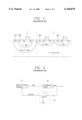
- a conventional CMOS twin-well process applied to semiconductor devices includes a P-well and an N-well that respectively receive a substrate voltage Vbb and a power source voltage Vcc.
- a related art triple-well process has been introduced to miniaturize the semiconductor devices and to improve reliability.
- the semiconductor device includes a memory cell unit 1 having a P-well surrounded by a deep N-well and a peripheral circuit unit 2 provided with a P-well and an N-well.
- a ground voltage Vss and a power source voltage Vcc are supplied to the P-well and the N-well, respectively, of the peripheral circuit unit 2.
- the power source voltage Vcc (not shown) or a boost voltage Vpp, and a substrate voltage Vbb are supplied to the deep N-well and the P-well, respectively, of the memory cell unit 1.
- a related art substrate voltage applying circuit in the semiconductor device supplies the substrate voltage Vbb to the P-well of the memory cell unit 1.
- FIG. 2 is a block diagram showing the related art substrate voltage applying circuit that includes an oscillation circuit 10 for generating an oscillation signal OSC and a pumping unit 20 for carrying out a voltage pumping operation in accordance with the oscillation signal OSC from the oscillation circuit 10 to generate the substrate voltage Vbb.
- a level sensing unit 30 senses a level of the substrate voltage Vbb outputted from the pumping unit 20 in accordance with a predetermined set sensing point and generates a sensing signal OSCSW.
- the oscillation circuit 10 and the pumping unit 20 can employ conventional devices. Accordingly, a detailed description is omitted.
- the level sensing unit 30 includes a sensing NMOS transistor N1 with a source and a substrate that receive the substrate voltage Vbb from the pumping unit 20.
- a gate of the sensing NMOS transistor N1 receives the ground voltage Vss and a drain is connected to the oscillation circuit 10.
- the sensing NMOS transistor N1 is located in the deep N-well of the memory cell unit 1 in FIG. 1.
- the pumping unit 20 performs the pumping operation in accordance with the oscillation signal OSC from the oscillation circuit 10 and supplies the substrate voltage Vbb to the memory cell unit 1.
- the level sensing unit 30 When the substrate voltage Vbb from the pumping unit 20 that is sensed by the level sensing unit 30 becomes a predetermined level, which is the sensing point, the level sensing unit 30 generates the sensing signal OSCSW to suspend the oscillation circuit 10.
- the level sensing unit 30 outputs the sensing signal OSCSW to continuously drive the oscillation circuit 10.
- the sensing point is a predetermined level.
- the sensing NMOS transistor N1 of the level sensing unit 30 is turned off.
- the oscillation circuit 10 is suspended.
- a level B of the substrate voltage Vbb is higher than the predetermined voltage level
- the sensing NMOS transistor N1 is turned on and outputs the substrate voltage Vbb. Accordingly, the oscillation circuit 10 is again operated.
- the sensing point or the predetermined voltage level of the level sensing unit 30 is determined by the turn-on voltage of the sensing NMOS transistor N1.
- the operation of the oscillation circuit 10 is controlled in accordance with the sensing signal OSCSW outputted from the level sensing unit 30.
- the substrate voltage applying circuit supplies the constant substrate voltage Vbb to the memory cell unit 1.
- the memory cell of the related art semiconductor device has the P-well that is in the deep N-well.
- the substrate voltage applying circuit is suspended, and a power source at a desirable level is externally applied to an substrate voltage input pad.
- the related art triple well memory cell and peripheral circuit and the related art substance voltage applying circuit have various disadvantages. Externally changing and supplying the substrate voltage when a semiconductor package is completely fabricated is difficult or impossible. Further, evaluation according to the substrate voltage is difficult or can not be achieved in the case of analyzing inferior memory cells and determining properties of memory cells.
- An object of the present invention is to provide a substrate voltage applying circuit that substantially obviates one or more of the problems caused by limitations and disadvantages of the related art.
- Another object of the present invention is to provide a substrate voltage applying circuit that selectively controls a substrate voltage level supplied to a semiconductor device.
- Another object of the present invention is to provide a substrate voltage applying circuit that selectively controls a substrate voltage level supplied to a memory cell unit of a semiconductor device by sensing substrate voltages with a plurality of prescribed sensing points.
- Another object of the present invention is to provide a substrate voltage applying circuit that selects a substrate voltage in accordance with an external sensing level selecting signal.
- Another object of the present invention is to provide a substrate voltage applying circuit that selectively generates a substrate voltage desired by a triple well semiconductor device.
- Another object of the present invention is to provide a substrate voltage generator that allows analysis of inferior memory cells to determine cell properties during testing.
- a circuit for controlling an oscillation circuit unit coupled to a pumping unit that provides a substrate voltage includes a level sense unit and a vendor test mode generating unit that codes input signals and outputs sense level selecting signals to the level sense unit, wherein the level sense unit senses a level of a substrate voltage by a plurality of prescribed sensing points and outputs a corresponding sensing signal for controlling the oscillation circuit according to the sense level selecting signals from the vendor test mode generating unit.
- a substrate voltage applying circuit of a semiconductor device includes a unit that applies a substrate voltage to the semiconductor device based on a first control signal, a generator unit that generates sense level selecting signals according to second control signals and a level sense unit coupled to the semiconductor device that senses a level of the substrate voltage using a plurality of prescribed sensing points and outputs the first control signal.
- FIG. 1 is a diagram showing cross-sectional view of a related art semiconductor device using a triple-well process
- FIG. 2 is a block diagram showing a related art substrate voltage applying circuit
- FIG. 3 is a diagram showing a sensing point of a level sensing unit in FIG. 2;
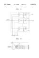
- FIG. 4 is a block diagram showing a preferred embodiment of a substrate voltage applying circuit according to the present invention.
- FIG. 5 is a circuit diagram showing a level sensing unit in FIG. 4.
- FIG. 6 is a diagram showing a plurality of sensing points of a level sensing unit in FIG. 4.
- FIG. 4 is a block diagram showing a preferred embodiment of a substrate voltage applying circuit according to the present invention.
- the preferred embodiment of the substrate voltage applying circuit includes an oscillation circuit unit 100, a pumping unit 200, a vendor test mode generating unit 300 and a level sensing unit 400.
- the oscillation circuit unit 100 and the pumping unit 200 can respectively use conventional circuits for an oscillating operation and for a pumping operation. Accordingly, a detailed description is omitted.
- the vendor test mode generating unit 300 codes a WCBR signal, a high level power source voltage SUPERVCC, and an address signal preferably received from external devices (not shown).
- the vendor test mode generating unit 300 generates sense level selecting signals DETa-DETn.
- FIG. 5 is a diagram that illustrates the level sensing unit 400.
- a plurality of level sense terminals 41a-41n are arranged in parallel between an input terminal and an output terminal.
- the level sense terminals 41a-41n respectively sense a substrate voltage Vbb from the pumping unit 200 and output a sensing signal OSCSW at a predetermined level in accordance with the corresponding sense level selecting signals DETa-DETn supplied from the vendor test mode generating unit 300.
- Each of the level sense terminals 41a-41n preferably includes a sensing NMOS transistor having a source and a substrate that receive the substrate voltage Vbb and a gate that receives a ground voltage Vss, and a switching NMOS transistor.
- Each of the switching NMOS transistors preferably has a source coupled to a drain of the sensing NMOS transistor, a drain coupled to the oscillation circuit unit 100, and a gate that receives a corresponding one of the sense level selecting signals DETa-DETn from the vendor test mode generating unit 300.
- the level sense terminal 41a includes NMOS sensing transistor N42 and NMOS switching transistor N43.
- each element is labeled with a different reference number.
- Sensing NMOS transistors N42, N44, N46 of the level sense terminals 41a -41n have a different size to obtain various sensing results of a variable level of the substrate voltage Vbb.
- the oscillation circuit unit 100 generates an oscillation signal OSC
- the pumping unit 200 pumps according to the oscillation signal OSC and supplies the substrate voltage Vbb to a memory cell unit.
- the level sense unit 400 senses a voltage level of the substrate voltage Vbb supplied from the pumping unit 200 by a plurality of sensing points and outputs a sensing signal OSCSW at a corresponding level to the oscillation circuit unit 100 in accordance with the sense level selecting signals DETa-DETn from the vendor test mode generating unit 300.
- the sensing points of the level sense unit 400 are determined for example by the different sized sensing NMOS transistors N42, N44, N46 in the level sense terminals 41a-41n. One of the level sense terminals 41a-41n is selected by the sense level selecting signals DETa-DETn.
- the switching NMOS transistor N43 of the level sense terminal 41a is turned on.
- the sensing signal OSCSW is outputted based on a sensing point determined by a size of the sensing NMOS transistor N42 of the selected level sense terminal 41a.
- the oscillation circuit unit 100 supplies the oscillation signal OSC or a suspending signal to the pumping unit 200 according to the sensing signal OSCSW. The above-described operation relates to the case where only the level sense terminal 41a is selected among the level sense terminals 41a-41n in accordance with the sense level selecting signals DETa-DETn from the vendor test mode generating unit 300.
- the sensing signal OSCSW of the level sense unit 400 is changed.
- the pumping unit 200 supplies the substrate voltage Vbb that has a different level from the previously generated substrate voltage Vbb to the memory cell unit.
- FIG. 6 illustrates various states of the level sense unit 400 in accordance with the sensing points that are selected by the sense level selecting signals DETa-DETn from the vendor test mode generating unit 300.
- sensing point 1 indicates general sensing points and sensing point 2 indicates sensing points that are arbitrarily controlled higher by the sense level selecting signals (DETa-DETn) from the vendor test mode generating unit 300.
- Sensing point 3 indicates sensing points that are arbitrarily controlled lower than the sensing point 1 by the sense level selecting signals (DEta-DEtn) from the vendor test mode generating unit 300.
- Sensing point 4 indicates sensing points that are arbitrarily controlled lower than sensing point 3 by the sense level selecting signals (DETa-DETn) from the vendor test mode generating unit 300. Accordingly, each of points A and B in FIG. 6 are sensing points at which the oscillation circuit unit 100 is preferably operated or suspended by changes of the sensing points.
- the vendor test mode generating unit 300 codes the WCBR signal, the high level power source voltage SUPERVCC, and the address signal, which are preferably externally supplied.
- the vendor test mode generating unit 300 further outputs the sense level selecting signals DETa-DETn to the level sense unit 400.
- the sense level selecting signals DETa-DETn supplied to the level sense unit 400 enable the switching NMOS transistors N43, N45, . . . , N47 of the level sense terminals 41a-41n to select the level sense terminal having the corresponding sensing point.
- the number of the level sense terminals 41a-41n is preferably determined by the number of bits of the sense level selecting signals DETa-DETn.
- the WCBR signal preferably indicates that a write enable signal is inputted before a CAS signal in the operation of a memory device, and the high level power source voltage SUPERVCC is an arbitrary voltage applied to a vendor test (e.g., over 6V).
- At least one level sense terminal 41a-41n is selected by the sense level selecting signals DETa-DETn from the vendor test mode generating unit 300, and a different sensing signal OSCSW is generated in accordance with the selected level sense terminal 41a-41n.
- the substrate voltage Vbb generated from the pumping unit 200 has a different level in accordance with the sense level selecting signals DETa-DETn from the vendor test mode generating unit 300. That is; although the semiconductor package is fabricated, the substrate voltage Vbb may be controlled to be lower or higher than a preset or initial level of a substrate voltage.
- the preferred embodiment of a substrate voltage applying circuit has various advantages.
- a level of the substrate voltage may be controlled even though the semiconductor package is completely fabricated.
- analyzing inferior memory cells and evaluating properties of memory cells can be performed using the preferred embodiment of a substrate voltage applying circuit. Further, yield and properties of the memory cells can be increased and improved, respectively.
Landscapes
- Engineering & Computer Science (AREA)
- Physics & Mathematics (AREA)
- Microelectronics & Electronic Packaging (AREA)
- Radar, Positioning & Navigation (AREA)
- Electromagnetism (AREA)
- General Physics & Mathematics (AREA)
- Nonlinear Science (AREA)
- Automation & Control Theory (AREA)
- Computer Hardware Design (AREA)
- Dram (AREA)
- Semiconductor Integrated Circuits (AREA)
- Logic Circuits (AREA)
- Metal-Oxide And Bipolar Metal-Oxide Semiconductor Integrated Circuits (AREA)
Abstract
Description
Claims (17)
Applications Claiming Priority (2)
| Application Number | Priority Date | Filing Date | Title |
|---|---|---|---|
| KR1019980003576A KR100300034B1 (en) | 1998-02-07 | 1998-02-07 | Substrate voltage source biasing circuit of semiconductor device |
| KR3576-98 | 1998-02-07 |
Publications (1)
| Publication Number | Publication Date |
|---|---|
| US6150870A true US6150870A (en) | 2000-11-21 |
Family
ID=19532686
Family Applications (1)
| Application Number | Title | Priority Date | Filing Date |
|---|---|---|---|
| US09/195,202 Expired - Lifetime US6150870A (en) | 1998-02-07 | 1998-11-18 | Adjustable substrate voltage applying circuit of a semiconductor device |
Country Status (3)
| Country | Link |
|---|---|
| US (1) | US6150870A (en) |
| JP (1) | JP4241974B2 (en) |
| KR (1) | KR100300034B1 (en) |
Cited By (4)
| Publication number | Priority date | Publication date | Assignee | Title |
|---|---|---|---|---|
| US6288963B1 (en) * | 1999-12-21 | 2001-09-11 | Fujitsu Limited | Semiconductor memory device |
| US20070145893A1 (en) * | 2005-11-14 | 2007-06-28 | Samsung Electronics Co., Ltd. | Display device |
| US20070273353A1 (en) * | 2006-05-09 | 2007-11-29 | Fujitsu Limited | Power supply sense circuit, power supply system and integrated circuit |
| US20080224684A1 (en) * | 2005-07-05 | 2008-09-18 | Freescale Semiconductor Inc. | Device and Method for Compensating for Voltage Drops |
Families Citing this family (1)
| Publication number | Priority date | Publication date | Assignee | Title |
|---|---|---|---|---|
| KR100317197B1 (en) * | 1999-12-27 | 2001-12-24 | 박종섭 | Substrate bias circuit |
Citations (7)
| Publication number | Priority date | Publication date | Assignee | Title |
|---|---|---|---|---|
| US4471290A (en) * | 1981-06-02 | 1984-09-11 | Tokyo Shibaura Denki Kabushiki Kaisha | Substrate bias generating circuit |
| US5744997A (en) * | 1995-04-26 | 1998-04-28 | Samsung Electronics, Co., Ltd. | Substrate bias voltage controlling circuit in semiconductor memory device |
| US5767735A (en) * | 1995-09-29 | 1998-06-16 | Intel Corporation | Variable stage charge pump |
| US5838189A (en) * | 1994-12-21 | 1998-11-17 | Samsung Electronics Co., Ltd. | Substrate voltage generating circuit of semiconductor memory device |
| US5929693A (en) * | 1996-02-05 | 1999-07-27 | Kabushiki Kaisha Toshiba | Substrate bias generator for semiconductor integrated circuit device |
| US5952872A (en) * | 1997-04-22 | 1999-09-14 | Lg Semicon Co., Ltd. | Input/output voltage detection type substrate voltage generation circuit |
| US6011743A (en) * | 1997-12-17 | 2000-01-04 | Lg Semicon Co., Ltd. | Charge pump circuit for memory device |
-
1998
- 1998-02-07 KR KR1019980003576A patent/KR100300034B1/en not_active IP Right Cessation
- 1998-11-12 JP JP32228898A patent/JP4241974B2/en not_active Expired - Fee Related
- 1998-11-18 US US09/195,202 patent/US6150870A/en not_active Expired - Lifetime
Patent Citations (7)
| Publication number | Priority date | Publication date | Assignee | Title |
|---|---|---|---|---|
| US4471290A (en) * | 1981-06-02 | 1984-09-11 | Tokyo Shibaura Denki Kabushiki Kaisha | Substrate bias generating circuit |
| US5838189A (en) * | 1994-12-21 | 1998-11-17 | Samsung Electronics Co., Ltd. | Substrate voltage generating circuit of semiconductor memory device |
| US5744997A (en) * | 1995-04-26 | 1998-04-28 | Samsung Electronics, Co., Ltd. | Substrate bias voltage controlling circuit in semiconductor memory device |
| US5767735A (en) * | 1995-09-29 | 1998-06-16 | Intel Corporation | Variable stage charge pump |
| US5929693A (en) * | 1996-02-05 | 1999-07-27 | Kabushiki Kaisha Toshiba | Substrate bias generator for semiconductor integrated circuit device |
| US5952872A (en) * | 1997-04-22 | 1999-09-14 | Lg Semicon Co., Ltd. | Input/output voltage detection type substrate voltage generation circuit |
| US6011743A (en) * | 1997-12-17 | 2000-01-04 | Lg Semicon Co., Ltd. | Charge pump circuit for memory device |
Non-Patent Citations (2)
| Title |
|---|
| Syuso Fujii, et al., "FAM 16.6: A 45ns 16Mb DRAM with Triple-Well Structure," Session 16; IEEE International Solid-State Circuits Conference, pp. 248-249, Feb. 1989. |
| Syuso Fujii, et al., FAM 16.6: A 45ns 16Mb DRAM with Triple Well Structure, Session 16; IEEE International Solid State Circuits Conference, pp. 248 249, Feb. 1989. * |
Cited By (6)
| Publication number | Priority date | Publication date | Assignee | Title |
|---|---|---|---|---|
| US6288963B1 (en) * | 1999-12-21 | 2001-09-11 | Fujitsu Limited | Semiconductor memory device |
| US20080224684A1 (en) * | 2005-07-05 | 2008-09-18 | Freescale Semiconductor Inc. | Device and Method for Compensating for Voltage Drops |
| US7956594B2 (en) * | 2005-07-05 | 2011-06-07 | Freescale Semiconductor, Inc. | Device and method for compensating for voltage drops |
| US20070145893A1 (en) * | 2005-11-14 | 2007-06-28 | Samsung Electronics Co., Ltd. | Display device |
| US7839366B2 (en) * | 2005-11-14 | 2010-11-23 | Samsung Electronics Co., Ltd. | Display device |
| US20070273353A1 (en) * | 2006-05-09 | 2007-11-29 | Fujitsu Limited | Power supply sense circuit, power supply system and integrated circuit |
Also Published As
| Publication number | Publication date |
|---|---|
| KR19990069372A (en) | 1999-09-06 |
| JPH11261013A (en) | 1999-09-24 |
| JP4241974B2 (en) | 2009-03-18 |
| KR100300034B1 (en) | 2001-09-06 |
Similar Documents
| Publication | Publication Date | Title |
|---|---|---|
| US7205682B2 (en) | Internal power supply circuit | |
| KR100292702B1 (en) | Semiconductor integrated circuit device capable of externally monitoring internal voltage | |
| KR0151032B1 (en) | The semiconductor memory device for package level dc voltage to be tested | |
| US6876585B2 (en) | Circuit and method for selecting reference voltages in semiconductor memory device | |
| JPH06295585A (en) | Inside power supply voltage generating circuit | |
| JPH05205469A (en) | Internal power-supply voltage generating circuit for semiconductor memory device | |
| MY122955A (en) | Method and apparatus for biasing selected and unselected array lines when writing a memory array | |
| US6150870A (en) | Adjustable substrate voltage applying circuit of a semiconductor device | |
| EP0473193A2 (en) | Semiconductor device having a temperature detection circuit | |
| KR100221799B1 (en) | Mode circuit and mode device | |
| US20050007187A1 (en) | Charge pump circuit operating responsive to a mode | |
| US20040239399A1 (en) | High voltage transfer circuit | |
| JP2000174081A (en) | Burn-in testing method of semiconductor chip, burn-in testing device, and semiconductor chip used for burn-in testing method | |
| KR19990060766A (en) | Internal Voltage Generation Circuit of Semiconductor Memory Device | |
| KR100414739B1 (en) | Internal voltage generator of semiconductor memory device | |
| US7626882B2 (en) | Flash memory device with external high voltage supply | |
| US6515934B2 (en) | Semiconductor device including internal potential generating circuit allowing tuning in short period of time and reduction of chip area | |
| US20030122590A1 (en) | Low voltage detector | |
| US6327178B1 (en) | Programmable circuit and its method of operation | |
| US5905682A (en) | Method and apparatus for biasing the substrate of an integrated circuit to an externally adjustable voltage | |
| KR100311972B1 (en) | Generation circuit of mode signal in semiconductor memory device | |
| US7164614B2 (en) | Fuse box, semiconductor memory device having the same and setting method thereof | |
| US6906967B2 (en) | Negative drop voltage generator in semiconductor memory device and method of controlling negative voltage generation | |
| KR20140025260A (en) | Integrated circuit chip | |
| US7250809B2 (en) | Boosted voltage generator |
Legal Events
| Date | Code | Title | Description |
|---|---|---|---|
| AS | Assignment |
Owner name: LG SEMICON CO., LTD., KOREA, REPUBLIC OF Free format text: ASSIGNMENT OF ASSIGNORS INTEREST;ASSIGNOR:KANG, DONG KEUM;REEL/FRAME:009593/0226 Effective date: 19981102 |
|
| AS | Assignment |
Owner name: HYUNDAI ELECTRONICS INDUSTRIES CO., LTD., KOREA, R Free format text: MERGER;ASSIGNOR:LG SEMICON CO., LTD.;REEL/FRAME:011014/0462 Effective date: 20000621 |
|
| STCF | Information on status: patent grant |
Free format text: PATENTED CASE |
|
| FEPP | Fee payment procedure |
Free format text: PAYOR NUMBER ASSIGNED (ORIGINAL EVENT CODE: ASPN); ENTITY STATUS OF PATENT OWNER: LARGE ENTITY |
|
| FPAY | Fee payment |
Year of fee payment: 4 |
|
| FPAY | Fee payment |
Year of fee payment: 8 |
|
| FEPP | Fee payment procedure |
Free format text: PAYOR NUMBER ASSIGNED (ORIGINAL EVENT CODE: ASPN); ENTITY STATUS OF PATENT OWNER: LARGE ENTITY Free format text: PAYER NUMBER DE-ASSIGNED (ORIGINAL EVENT CODE: RMPN); ENTITY STATUS OF PATENT OWNER: LARGE ENTITY |
|
| AS | Assignment |
Owner name: HYNIX SEMICONDUCTOR INC., KOREA, REPUBLIC OF Free format text: CHANGE OF NAME;ASSIGNOR:HYUNDAI ELECTRONICS INDUSTRIES CO., LTD.;REEL/FRAME:026828/0688 Effective date: 20010329 |
|
| AS | Assignment |
Owner name: 658868 N.B. INC., CANADA Free format text: ASSIGNMENT OF ASSIGNORS INTEREST;ASSIGNOR:HYNIX SEMICONDUCTOR INC.;REEL/FRAME:027234/0243 Effective date: 20110822 |
|
| FEPP | Fee payment procedure |
Free format text: PAYOR NUMBER ASSIGNED (ORIGINAL EVENT CODE: ASPN); ENTITY STATUS OF PATENT OWNER: LARGE ENTITY Free format text: PAYER NUMBER DE-ASSIGNED (ORIGINAL EVENT CODE: RMPN); ENTITY STATUS OF PATENT OWNER: LARGE ENTITY |
|
| AS | Assignment |
Owner name: ROYAL BANK OF CANADA, CANADA Free format text: U.S. INTELLECTUAL PROPERTY SECURITY AGREEMENT (FOR NON-U.S. GRANTORS) - SHORT FORM;ASSIGNORS:658276 N.B. LTD.;658868 N.B. INC.;MOSAID TECHNOLOGIES INCORPORATED;REEL/FRAME:027512/0196 Effective date: 20111223 |
|
| FPAY | Fee payment |
Year of fee payment: 12 |
|
| AS | Assignment |
Owner name: CONVERSANT IP N.B. 868 INC., CANADA Free format text: CHANGE OF NAME;ASSIGNOR:658868 N.B. INC.;REEL/FRAME:032439/0547 Effective date: 20140101 |
|
| AS | Assignment |
Owner name: CONVERSANT INTELLECTUAL PROPERTY MANAGEMENT INC., Free format text: RELEASE OF SECURITY INTEREST;ASSIGNOR:ROYAL BANK OF CANADA;REEL/FRAME:033484/0344 Effective date: 20140611 Owner name: CONVERSANT IP N.B. 868 INC., CANADA Free format text: RELEASE OF SECURITY INTEREST;ASSIGNOR:ROYAL BANK OF CANADA;REEL/FRAME:033484/0344 Effective date: 20140611 Owner name: CONVERSANT IP N.B. 276 INC., CANADA Free format text: RELEASE OF SECURITY INTEREST;ASSIGNOR:ROYAL BANK OF CANADA;REEL/FRAME:033484/0344 Effective date: 20140611 |
|
| AS | Assignment |
Owner name: ROYAL BANK OF CANADA, AS LENDER, CANADA Free format text: U.S. PATENT SECURITY AGREEMENT (FOR NON-U.S. GRANTORS);ASSIGNOR:CONVERSANT IP N.B. 868 INC.;REEL/FRAME:033707/0001 Effective date: 20140611 Owner name: CPPIB CREDIT INVESTMENTS INC., AS LENDER, CANADA Free format text: U.S. PATENT SECURITY AGREEMENT (FOR NON-U.S. GRANTORS);ASSIGNOR:CONVERSANT IP N.B. 868 INC.;REEL/FRAME:033707/0001 Effective date: 20140611 |
|
| AS | Assignment |
Owner name: CONVERSANT INTELLECTUAL PROPERTY MANAGEMENT INC., Free format text: ASSIGNMENT OF ASSIGNORS INTEREST;ASSIGNOR:CONVERSANT IP N.B. 868 INC.;REEL/FRAME:036159/0386 Effective date: 20150514 |
|
| AS | Assignment |
Owner name: CPPIB CREDIT INVESTMENTS, INC., CANADA Free format text: AMENDED AND RESTATED U.S. PATENT SECURITY AGREEMENT (FOR NON-U.S. GRANTORS);ASSIGNOR:CONVERSANT INTELLECTUAL PROPERTY MANAGEMENT INC.;REEL/FRAME:046900/0136 Effective date: 20180731 |
|
| AS | Assignment |
Owner name: CONVERSANT INTELLECTUAL PROPERTY MANAGEMENT INC., CANADA Free format text: RELEASE OF U.S. PATENT AGREEMENT (FOR NON-U.S. GRANTORS);ASSIGNOR:ROYAL BANK OF CANADA, AS LENDER;REEL/FRAME:047645/0424 Effective date: 20180731 Owner name: CONVERSANT INTELLECTUAL PROPERTY MANAGEMENT INC., Free format text: RELEASE OF U.S. PATENT AGREEMENT (FOR NON-U.S. GRANTORS);ASSIGNOR:ROYAL BANK OF CANADA, AS LENDER;REEL/FRAME:047645/0424 Effective date: 20180731 |
|
| AS | Assignment |
Owner name: CONVERSANT INTELLECTUAL PROPERTY MANAGEMENT INC., CANADA Free format text: RELEASE BY SECURED PARTY;ASSIGNOR:CPPIB CREDIT INVESTMENTS INC.;REEL/FRAME:054371/0884 Effective date: 20201028 |