US6147562A - Apparatus for synchronizing master and slave processors - Google Patents

Apparatus for synchronizing master and slave processors Download PDF

Info

Publication number
US6147562A
US6147562A US09/308,947 US30894799A US6147562A US 6147562 A US6147562 A US 6147562A US 30894799 A US30894799 A US 30894799A US 6147562 A US6147562 A US 6147562A
Authority
US
United States
Prior art keywords
input
phase
signals
system clock
signal
Prior art date
Legal status (The legal status is an assumption and is not a legal conclusion. Google has not performed a legal analysis and makes no representation as to the accuracy of the status listed.)
Expired - Fee Related
Application number
US09/308,947
Inventor
Gerhard Quirmbach
Current Assignee (The listed assignees may be inaccurate. Google has not performed a legal analysis and makes no representation or warranty as to the accuracy of the list.)
Nokia Solutions and Networks GmbH and Co KG
Original Assignee
Siemens AG
Priority date (The priority date is an assumption and is not a legal conclusion. Google has not performed a legal analysis and makes no representation as to the accuracy of the date listed.)
Filing date
Publication date
Application filed by Siemens AG filed Critical Siemens AG
Assigned to SIEMENS AKTIENGESELLSCHAFT reassignment SIEMENS AKTIENGESELLSCHAFT ASSIGNMENT OF ASSIGNORS INTEREST (SEE DOCUMENT FOR DETAILS). Assignors: QUIRMBACH, GERHARD
Application granted granted Critical
Publication of US6147562A publication Critical patent/US6147562A/en
Assigned to NOKIA SIEMENS NETWORKS GMBH & CO. KG reassignment NOKIA SIEMENS NETWORKS GMBH & CO. KG ASSIGNMENT OF ASSIGNORS INTEREST (SEE DOCUMENT FOR DETAILS). Assignors: SIEMENS AKTIENGESELLSCHAFT
Anticipated expiration legal-status Critical
Expired - Fee Related legal-status Critical Current

Links

Images

Classifications

    • HELECTRICITY
    • H03ELECTRONIC CIRCUITRY
    • H03LAUTOMATIC CONTROL, STARTING, SYNCHRONISATION, OR STABILISATION OF GENERATORS OF ELECTRONIC OSCILLATIONS OR PULSES
    • H03L7/00Automatic control of frequency or phase; Synchronisation
    • H03L7/06Automatic control of frequency or phase; Synchronisation using a reference signal applied to a frequency- or phase-locked loop
    • H03L7/07Automatic control of frequency or phase; Synchronisation using a reference signal applied to a frequency- or phase-locked loop using several loops, e.g. for redundant clock signal generation
    • HELECTRICITY
    • H03ELECTRONIC CIRCUITRY
    • H03LAUTOMATIC CONTROL, STARTING, SYNCHRONISATION, OR STABILISATION OF GENERATORS OF ELECTRONIC OSCILLATIONS OR PULSES
    • H03L7/00Automatic control of frequency or phase; Synchronisation
    • H03L7/06Automatic control of frequency or phase; Synchronisation using a reference signal applied to a frequency- or phase-locked loop
    • H03L7/08Details of the phase-locked loop
    • H03L7/085Details of the phase-locked loop concerning mainly the frequency- or phase-detection arrangement including the filtering or amplification of its output signal
    • H03L7/087Details of the phase-locked loop concerning mainly the frequency- or phase-detection arrangement including the filtering or amplification of its output signal using at least two phase detectors or a frequency and phase detector in the loop

Definitions

  • the present invention related generally to a synchronization unit for synchronizing two system clocks in an electronic device, such as a switching device.
  • two processor assemblies (one of the two is a master and the other is a slave) work redundantly.
  • This can be achieved by micro-synchronous operation, whereby the slave synchronizes to the master.
  • the master in turn synchronizes to an external reference clock. Given an outage of the external reference clock, the (clock) master must continue to work for example, in a (hold over mode) and the slave must continue to synchronize to the master.
  • phase difference between the two processor assemblies should lie within an extremely slight time difference (for example, 5 ns).
  • the European patent document EP 0 175 888 A discloses a synchronization means using a phase comparator with each incoming channel to compare the clock phase of the incoming signal and a local oscillator.
  • the phase comparator of the active unit generates a signal to control the oscillator to maintain its output in phase with incoming signal.
  • the oscillator is a voltage controlled quartz oscillator.
  • the present invention is based on the object of providing a synchronization portion of an assembly that meets the demand for collaboration with the synchronization portion of a partner assembly.
  • a synchronization portion of an assembly that generates the system clock of the assembly, whereby it synchronizes the system clock to one of several existing reference clocks, including,
  • a VCO that generates the system clock of the assembly depending on a signal applied to its control input
  • an operating control that controls the switches following the filters such that respectively one of the output signals of the filters is through-connected to the control input of the VCO, the operating control controls further switches such that, given the arrangement wherein the output signal of the filter is not through-connected to the input of the VCO,
  • the output of the phase detector is switched to tri-state
  • the output signal is fed back to the one filter input
  • the decoupled signal of the control input of the VCO is applied to the other filter input.
  • One embodiment of the invention provides a delay unit that delays the system clock before the input to the phase detector by the running time difference between reference clock and system clock which makes it possible to switch the mode of a processor assembly (for example, from clock master to clock slave or vice versa) without leaving the micro-synchronous operation (slave/slave is not possible). The switching is thus possible during micro-synchronous operation.
  • FIG. 1 is a block diagram showing the synchronization system of the present invention in a master/slave processor arrangement
  • FIG. 2 is functional block diagram of the synchronization portion
  • FIG. 3 is a circuit diagram showing the activated operating mode
  • FIG. 4 is a circuit diagram showing the standby mode
  • FIG. 5 is a circuit diagram showing the circuit in the monitor mode.
  • FIG. 1 shows the basic structure of the mutual clock synchronization.
  • a respective PLL is contained in an assembly, a switch that serves for switching between the operating modes "Master” and “Slave” of an assembly being present at the input thereof.
  • the Slave Assembly synchronizes to the Master Processor assembly with a PLL (Phase Locked Loop).
  • PLL Phase Locked Loop
  • FIG. 2 shows the basic structure of an inventive synchronization means.
  • the synchronization means comprises
  • VCO voltage controlled oscillator
  • phase detector RV with a following filter (a loop filter) and that is provided for each reference clock, whereby a respective reference clock signal is at the one input R of a phase detector and the system clock is respectively adjacent at the other input V,
  • an operations controller (OC; can, for example, be realized by the processor of the assembly and/or by a corresponding logic) unit that controls the switches following the filters such that respectively one of the output signals of the filters is through-connected to the control input of the VCO,
  • a delay unit (shown as a delay line) that delays the system clock preceding the input to the phase detector by the running time difference between the reference clock and the system clock.
  • the selection of the reference clocks by (analog) switches at the set voltage input of the VCO is for the following reason. Due to the demand of a maximum 5 ns phase difference between the Master and the Slave, no further running time of any switches whatsoever for the selection of an external reference clock is allowed preceding the input of the phase comparator of the "Partner Processor Assembly" other than the line running time (the time difference between the minimum and the maximum running time of such a switch, namely, deteriorates the worst case phase difference between the Master assembly and the Slave assembly). A separate phase comparator is therefore inventively present for each reference clock.
  • a delay unit (which here is a delay line) is inserted preceding the comparison input V of the phase detector of the Partner Processing Assembly that delays the system clock preceding the input to the phase detector by the running time difference between the reference clock on the Master assembly and the system clock of the Slave assembly.
  • the operating control also controls further switches (shown in FIGS. 3-5) such that, given a filter whose output signal is not through-connected to the input of the VCO, the output signal is fed back to the one filter input and the decoupled signal of the control input of the VCO is applied to the other filter input.
  • the output signal of a passively co-running loop filter is constantly regulated to the same level as that of the active arrangement.
  • An optimum transient response of the PLL phase skip thereby derives after the switching to a different reference clock (external reference clock or system clock of the Partner assembly)! A mode switching and/or a change of the external clock source is thus possible without deterioration of the micro-synchronous operation.
  • the inventive clock synchronization works without exchange of the phase information. This is achieved in that the line running time between the two processor assemblies is compensated with a lead of the PLL.
  • the selected PLL has a zero phase difference at the input of a phase detector (PD) between the local clock and the external reference clock.
  • PD phase detector
  • phase detector PD-Type 4 from Roland Best, theory und für des Phase-locked Loops, ISBN 3-85502-132-5 can be taken as a phase detector and can be easily modified so that it synchronizes to the positive signal edge and the two outputs can be switched to tri-state.
  • the advantage of this type is:
  • a slow transient response is required when switching to an external reference.
  • the modulation of the set voltage input of the VCO must therefore be small (small amplification) at the input phase skip.
  • a fast transient response is required when switching to the Partner processor assembly.
  • the modulation of the set voltage input of the VCO must therefore be great (great amplification) at the input phase skip.
  • FIG. 3 shows the activated operating mode
  • the PLL control circuit In this operating mode, the PLL control circuit is closed (D1 and U1 are not applied to tri-state).
  • the processor assembly can thereby be in Master mode or Slave mode.
  • FIG. 4 shows the holdover operating mode
  • the processor assembly In this operating mode, the processor assembly is in the Master mode and works without an external reference. In this operating mode, the output of the loop filter amounts to 1.5 V.
  • FIG. 5 shows the monitor VCO operating mode
  • the output voltage value of the loop filter corresponds to the voltage value at the VCO set voltage input.
  • the correct output level is assured at the VCO set voltage input at the moment of switching to the activated mode (PLL control circuit) (an output level at the positive or negative detent of the operational amplifier would result in a frequency skip that could lead to the upward transgression of the 5 ns maximum phase difference demand between two processor assemblies).

Abstract

A master and slave arrangement of processors includes a clock signal synchronization apparatus. The clock signals of two (processor) assemblies in micro-synchronous operation are only allowed to exhibit an extremely slight phase difference. A system clock signal is generated by a voltage controlled oscillator, which is fed by phase detectors with a filter at the output of each phase detector. Switches are provided between the filter output and the voltage controlled oscillator input. The phase detectors compare the system clock signal and a reference clock signal. A delay is provided at the input of one phase detector.

Description

BACKGROUND OF THE INVENTION
1. Field of the Invention
The present invention related generally to a synchronization unit for synchronizing two system clocks in an electronic device, such as a switching device.
2. Description of the Related Art
For satisfying increased operational dependability in switching technology, it is demanded that two processor assemblies (one of the two is a master and the other is a slave) work redundantly. This can be achieved by micro-synchronous operation, whereby the slave synchronizes to the master. The master in turn synchronizes to an external reference clock. Given an outage of the external reference clock, the (clock) master must continue to work for example, in a (hold over mode) and the slave must continue to synchronize to the master.
The critical demand for micro-synchronous operation is that the phase difference between the two processor assemblies should lie within an extremely slight time difference (for example, 5 ns).
Synchronization methods wherein phase information are exchanged between the two processor assemblies can be imagined for satisfying the demand. In these methods, however, falsifications of the phase information can occur due to different gate running times and reflections on the connecting lines between the two assemblies. This leads to operating instabilities.
The European patent document EP 0 175 888 A discloses a synchronization means using a phase comparator with each incoming channel to compare the clock phase of the incoming signal and a local oscillator. The phase comparator of the active unit generates a signal to control the oscillator to maintain its output in phase with incoming signal. The oscillator is a voltage controlled quartz oscillator.
SUMMARY OF THE INVENTION
The present invention is based on the object of providing a synchronization portion of an assembly that meets the demand for collaboration with the synchronization portion of a partner assembly.
This object is achieved by a synchronization portion of an assembly that generates the system clock of the assembly, whereby it synchronizes the system clock to one of several existing reference clocks, including,
a) a VCO that generates the system clock of the assembly depending on a signal applied to its control input;
b) an arrangement that includes a phase detector with a following filter and is present respectively once per reference clock signal, whereby a respective reference clock signal is applied to one input of a phase detector and the system clock is respectively applied to the other input;
c) an operating control that controls the switches following the filters such that respectively one of the output signals of the filters is through-connected to the control input of the VCO, the operating control controls further switches such that, given the arrangement wherein the output signal of the filter is not through-connected to the input of the VCO,
the output of the phase detector is switched to tri-state;
the output signal is fed back to the one filter input; and
the decoupled signal of the control input of the VCO is applied to the other filter input.
One embodiment of the invention provides a delay unit that delays the system clock before the input to the phase detector by the running time difference between reference clock and system clock which makes it possible to switch the mode of a processor assembly (for example, from clock master to clock slave or vice versa) without leaving the micro-synchronous operation (slave/slave is not possible). The switching is thus possible during micro-synchronous operation.
BRIEF DESCRIPTION OF THE DRAWINGS
An exemplary embodiment of the invention is explained in greater detail below with reference to the drawings.
FIG. 1 is a block diagram showing the synchronization system of the present invention in a master/slave processor arrangement;
FIG. 2 is functional block diagram of the synchronization portion;
FIG. 3 is a circuit diagram showing the activated operating mode;
FIG. 4 is a circuit diagram showing the standby mode; and
FIG. 5 is a circuit diagram showing the circuit in the monitor mode.
DETAILED DESCRIPTION OF THE PREFERRED EMBODIMENTS
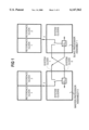
FIG. 1 shows the basic structure of the mutual clock synchronization. According to the illustrated structure, a respective PLL is contained in an assembly, a switch that serves for switching between the operating modes "Master" and "Slave" of an assembly being present at the input thereof.
Only one processor assembly is synchronized to the external reference clock, namely the master assembly. The other processor assembly which is referred to as the "Slave Assembly" synchronizes to the Master Processor assembly with a PLL (Phase Locked Loop). The Slave Processor assembly runs with exactly the same frequency and phase as the Master Processor assembly.
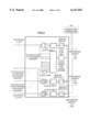
FIG. 2 shows the basic structure of an inventive synchronization means. The synchronization means comprises
a voltage controlled oscillator VCO that generates the system clock signal of the assembly dependent on a signal adjacent at its control input which here is a (set voltage input),
an arrangement that comprises a phase detector RV with a following filter (a loop filter) and that is provided for each reference clock, whereby a respective reference clock signal is at the one input R of a phase detector and the system clock is respectively adjacent at the other input V,
an operations controller (OC; can, for example, be realized by the processor of the assembly and/or by a corresponding logic) unit that controls the switches following the filters such that respectively one of the output signals of the filters is through-connected to the control input of the VCO,
a delay unit (shown as a delay line) that delays the system clock preceding the input to the phase detector by the running time difference between the reference clock and the system clock.
The selection of the reference clocks by (analog) switches at the set voltage input of the VCO (see FIG. 2) is for the following reason. Due to the demand of a maximum 5 ns phase difference between the Master and the Slave, no further running time of any switches whatsoever for the selection of an external reference clock is allowed preceding the input of the phase comparator of the "Partner Processor Assembly" other than the line running time (the time difference between the minimum and the maximum running time of such a switch, namely, deteriorates the worst case phase difference between the Master assembly and the Slave assembly). A separate phase comparator is therefore inventively present for each reference clock.
The advantage of the structure shown in FIG. 2 compared to the arrangement shown in FIG. 1 wherein the switches are arranged at the input of the PLLs is thus comprised therein that no further running time of any switches whatsoever for the selection of an external reference clock is added to the phase difference.
If the line running time makes an unacceptable difference with respect to the demand made of the phase time difference, this can be compensated with a lead of the PLL. To that end, a delay unit (which here is a delay line) is inserted preceding the comparison input V of the phase detector of the Partner Processing Assembly that delays the system clock preceding the input to the phase detector by the running time difference between the reference clock on the Master assembly and the system clock of the Slave assembly. Given employment of such a delay unit, what one thus achieves is that the reference clock and system clock (given selection of a PLL that controls the phase difference at the phase detector input to zero) are practically equiphase independently of the running time difference.
In addition to controlling the switches shown in FIG. 2, the operating control also controls further switches (shown in FIGS. 3-5) such that, given a filter whose output signal is not through-connected to the input of the VCO, the output signal is fed back to the one filter input and the decoupled signal of the control input of the VCO is applied to the other filter input. As a result thereof, the output signal of a passively co-running loop filter is constantly regulated to the same level as that of the active arrangement. An optimum transient response of the PLL phase skip thereby derives after the switching to a different reference clock (external reference clock or system clock of the Partner assembly)! A mode switching and/or a change of the external clock source is thus possible without deterioration of the micro-synchronous operation.
The inventive clock synchronization works without exchange of the phase information. This is achieved in that the line running time between the two processor assemblies is compensated with a lead of the PLL.
The selected PLL has a zero phase difference at the input of a phase detector (PD) between the local clock and the external reference clock.
For example, the phase detector PD-Type 4 from Roland Best, Theorie und Anwendung des Phase-locked Loops, ISBN 3-85502-132-5 can be taken as a phase detector and can be easily modified so that it synchronizes to the positive signal edge and the two outputs can be switched to tri-state. The advantage of this type is:
control to zero phase difference
phase and frequency-sensitive behavior
independence from supply voltage and temperature
easy realizability of the three phase comparators in one PLD (Programmable Logic Device)
great range of theoretical ±2π. This is necessary since the phase is not lost given switching to a different reference clock, i.e. synchronization is carried out to the original signal edge when switching back. This is necessary in order to prevent data loss at the synchronous TSI interface.
Loop Filter:
Three loop filters having the following properties are realized:
A slow transient response is required when switching to an external reference. The modulation of the set voltage input of the VCO must therefore be small (small amplification) at the input phase skip.
A fast transient response is required when switching to the Partner processor assembly. The modulation of the set voltage input of the VCO must therefore be great (great amplification) at the input phase skip.
Different frequencies at the input of the three phase comparators, finally, likewise require correspondingly different dimensionings of the loop filters.
In order to prevent the loop filter output from leaving the range of the operating voltage and proceeding into saturation (detent of the output voltage has a negative influence on the transient response of the PLL), there are three operating modes for each loop filter, these being shown in FIGS. 3-5 and being controlled by the operating control with the assistance of the illustrated switches.
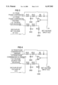
FIG. 3 shows the activated operating mode:
In this operating mode, the PLL control circuit is closed (D1 and U1 are not applied to tri-state). The processor assembly can thereby be in Master mode or Slave mode.
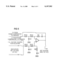
FIG. 4 shows the holdover operating mode:
In this operating mode, the processor assembly is in the Master mode and works without an external reference. In this operating mode, the output of the loop filter amounts to 1.5 V.
FIG. 5 shows the monitor VCO operating mode:
In this operating mode, the output voltage value of the loop filter corresponds to the voltage value at the VCO set voltage input. As a result thereof, the correct output level is assured at the VCO set voltage input at the moment of switching to the activated mode (PLL control circuit) (an output level at the positive or negative detent of the operational amplifier would result in a frequency skip that could lead to the upward transgression of the 5 ns maximum phase difference demand between two processor assemblies).
Although other modifications and changes may be suggested by those skilled in the art, it is the intention of the inventors to embody within the patent warranted hereon all changes and modifications as reasonably and properly come within the scope of their contribution to the art.

Claims (3)

What is claimed is:
1. A synchronization apparatus of an assembly that generates a system clock signal which is synchronized to one of a plurality of reference clocks, comprising:
a voltage controlled oscillator having a control input and that generates the system clock signal of the assembly dependent on a signal at said control input;
an arrangement including phase detectors each having two inputs and an output, a respective reference clock signal applied to one of said two inputs of each of said phase detectors and the system clock signal being applied to the other of said two inputs;
filters having inputs connected to said outputs of said phase detectors and having outputs;
switches connected at said outputs of said filters to connect signals output from said filters to said control input of said voltage controlled oscillator;
an operating controller connected to said switches that controls said switches such that respectively one of the output signals of the filters is through-connected to the control input of the VCO, and
further switches connected to said operating controller which controls said further switches such that, given a case wherein the output signal of a respective one of the filters is not through-connected to the input of the VCO,
the output of a respective on of the phase detectors is switched to tri-state;
the output signal is fed back to a first input of said respective one of said filters;
and a decoupled signal of the control input of the VCO is applied to a second input of said respective one of said filters.
2. A synchronization unit according to claim 1, further comprising:
a delay unit that delays the system clock before input to a phase detector of the phase detectors by a running time difference between the reference clock of the phase detector of the phase detectors and the system clock.
3. A method for synchronizing clock signals in a master/slave arrangement, comprising the steps of:
generating a system clock signal depending on an input control signal;
providing reference clock signals;
detecting a phase difference between each of the reference clock signals and the system clock signal to obtain phase difference signals;
filtering said phase difference signals with a filter to obtain filter signals;
selectively connecting one of said filter signals as said input control signal;
providing a tri-state output of said phase difference detecting step;
feeding said filter signals of said filtering step back to a further filter to synchronize said system clock to one of a plurality of reference clocks.
US09/308,947 1996-11-26 1997-11-04 Apparatus for synchronizing master and slave processors Expired - Fee Related US6147562A (en)

Applications Claiming Priority (2)

Application Number Priority Date Filing Date Title
EP96118915 1996-11-26
PCT/EP1997/006080 WO1998024185A1 (en) 1996-11-26 1997-11-04 Synchronisation unit for a component group

Publications (1)

Publication Number Publication Date
US6147562A true US6147562A (en) 2000-11-14

Family

ID=8223432

Family Applications (1)

Application Number Title Priority Date Filing Date
US09/308,947 Expired - Fee Related US6147562A (en) 1996-11-26 1997-11-04 Apparatus for synchronizing master and slave processors

Country Status (6)

Country Link
US (1) US6147562A (en)
EP (1) EP0941580B1 (en)
CN (1) CN1126255C (en)
CA (1) CA2272658A1 (en)
DE (1) DE59706267D1 (en)
WO (1) WO1998024185A1 (en)

Cited By (4)

* Cited by examiner, † Cited by third party
Publication number Priority date Publication date Assignee Title
EP1271788A2 (en) * 2001-06-29 2003-01-02 Motorola, Inc. Circuits for use in radio communications
WO2007124788A1 (en) * 2006-01-10 2007-11-08 Rohde & Schwarz Gmbh & Co. Kg Apparatus for phase synchronisation according to the master/slave principle
US20100134159A1 (en) * 2008-11-28 2010-06-03 Zarlink Semiconductor Inc. Soft reference switch for phase locked loop
US7826519B1 (en) * 2005-05-23 2010-11-02 Marvell International, Ltd Method and apparatus for providing coherent phase noise in transceivers or similar systems

Families Citing this family (1)

* Cited by examiner, † Cited by third party
Publication number Priority date Publication date Assignee Title
CN102075314A (en) * 2009-11-24 2011-05-25 航天信息股份有限公司 Time synchronization method of network tax control system

Citations (6)

* Cited by examiner, † Cited by third party
Publication number Priority date Publication date Assignee Title
US4511859A (en) * 1982-08-30 1985-04-16 At&T Bell Laboratories Apparatus for generating a common output signal as a function of any of a plurality of diverse input signals
EP0139126A2 (en) * 1981-06-08 1985-05-02 BRITISH TELECOMMUNICATIONS public limited company Phase-locked loops and electrical networks incorporating them
EP0175888A2 (en) * 1984-09-25 1986-04-02 Siemens Telecomunicazioni S.P.A. Circuit for limiting jitter transients during switching
EP0262481A2 (en) * 1986-09-30 1988-04-06 Siemens Aktiengesellschaft Circuit arrangement for the generation of a clock signal synchronised with an applied reference frequency
US5216387A (en) * 1991-09-10 1993-06-01 John Fluke Mfg. Co., Inc. Noise reduction method and apparatus for phase-locked loops
US5739727A (en) * 1995-10-05 1998-04-14 Telefonaktiebolaget Lm Ericsson Sampled phase locked loop being locked with support from another phase locked loop

Patent Citations (6)

* Cited by examiner, † Cited by third party
Publication number Priority date Publication date Assignee Title
EP0139126A2 (en) * 1981-06-08 1985-05-02 BRITISH TELECOMMUNICATIONS public limited company Phase-locked loops and electrical networks incorporating them
US4511859A (en) * 1982-08-30 1985-04-16 At&T Bell Laboratories Apparatus for generating a common output signal as a function of any of a plurality of diverse input signals
EP0175888A2 (en) * 1984-09-25 1986-04-02 Siemens Telecomunicazioni S.P.A. Circuit for limiting jitter transients during switching
EP0262481A2 (en) * 1986-09-30 1988-04-06 Siemens Aktiengesellschaft Circuit arrangement for the generation of a clock signal synchronised with an applied reference frequency
US5216387A (en) * 1991-09-10 1993-06-01 John Fluke Mfg. Co., Inc. Noise reduction method and apparatus for phase-locked loops
US5739727A (en) * 1995-10-05 1998-04-14 Telefonaktiebolaget Lm Ericsson Sampled phase locked loop being locked with support from another phase locked loop

Cited By (9)

* Cited by examiner, † Cited by third party
Publication number Priority date Publication date Assignee Title
EP1271788A2 (en) * 2001-06-29 2003-01-02 Motorola, Inc. Circuits for use in radio communications
US6717484B2 (en) * 2001-06-29 2004-04-06 Motorola, Inc. Circuits for use in radio communications
EP1271788A3 (en) * 2001-06-29 2004-10-20 Motorola, Inc. Circuits for use in radio communications
US7826519B1 (en) * 2005-05-23 2010-11-02 Marvell International, Ltd Method and apparatus for providing coherent phase noise in transceivers or similar systems
WO2007124788A1 (en) * 2006-01-10 2007-11-08 Rohde & Schwarz Gmbh & Co. Kg Apparatus for phase synchronisation according to the master/slave principle
US20090096536A1 (en) * 2006-01-10 2009-04-16 Rhode & Schwarz Gmbh & Co. Kg Arrangement for Phase Synchronization According to the Master/Slave Principle
US7772928B2 (en) 2006-01-10 2010-08-10 Rohde & Schwarz Gmbh & Co. Kg Arrangement for phase synchronization according to the master/slave principle
US20100134159A1 (en) * 2008-11-28 2010-06-03 Zarlink Semiconductor Inc. Soft reference switch for phase locked loop
US7965115B2 (en) 2008-11-28 2011-06-21 Zarlink Semiconductor Inc. Soft reference switch for phase locked loop

Also Published As

Publication number Publication date
CN1238863A (en) 1999-12-15
WO1998024185A1 (en) 1998-06-04
DE59706267D1 (en) 2002-03-14
CN1126255C (en) 2003-10-29
EP0941580B1 (en) 2002-01-30
CA2272658A1 (en) 1998-06-04
EP0941580A1 (en) 1999-09-15

Similar Documents

Publication Publication Date Title
JP3255418B2 (en) Digitally controlled crystal oscillator
KR20070049566A (en) Switchable pll circuit
JP2003051742A (en) Clock generating circuit
JPH06102964A (en) Information processing system
JP3615734B2 (en) Circuit device for generating clock signal frequency-synchronized with reference clock signal
US5530726A (en) Method and apparatus for switching of duplexed clock system
US6147562A (en) Apparatus for synchronizing master and slave processors
CN100438361C (en) Method for controlling master spare clock phase for synchronous digital system equipment
KR100212139B1 (en) Clock supplying apparatus
KR940002449B1 (en) Modulating method phase and frequency of pll
US5867545A (en) Phase-locked loop circuit
KR100328757B1 (en) A error preventing device of clock signal with switchover for transmission system
KR20000061197A (en) Apparatus and method for controlling clock frequency using plural phase-locked loops
JP2725530B2 (en) Clock supply method
KR100262945B1 (en) Digital Pll Control Method which using transition mode for synchronizing
KR100282410B1 (en) System clock board
JPH0267820A (en) Standard frequency clock generator
JPH0964732A (en) Synchronization clock generating circuit
JP3160904B2 (en) Phase-locked oscillation circuit device
KR920003362B1 (en) Method and an apparatus for compensating fine phase difference of clock signals
KR100518439B1 (en) Apparatus for Synchronizing Phase of duplicated Clock Module
JPH1127247A (en) System switching method
KR100328761B1 (en) A device of switching system clock unit for optical communication system
JPH11298460A (en) Clock changeover circuit
KR19980085920A (en) Transfer Clock Synchronizer and Phase Compensation Circuit

Legal Events

Date Code Title Description
AS Assignment

Owner name: SIEMENS AKTIENGESELLSCHAFT, GERMANY

Free format text: ASSIGNMENT OF ASSIGNORS INTEREST;ASSIGNOR:QUIRMBACH, GERHARD;REEL/FRAME:010079/0170

Effective date: 19971020

FEPP Fee payment procedure

Free format text: PAYOR NUMBER ASSIGNED (ORIGINAL EVENT CODE: ASPN); ENTITY STATUS OF PATENT OWNER: LARGE ENTITY

FPAY Fee payment

Year of fee payment: 4

AS Assignment

Owner name: NOKIA SIEMENS NETWORKS GMBH & CO. KG, GERMANY

Free format text: ASSIGNMENT OF ASSIGNORS INTEREST;ASSIGNOR:SIEMENS AKTIENGESELLSCHAFT;REEL/FRAME:020593/0160

Effective date: 20080107

REMI Maintenance fee reminder mailed
LAPS Lapse for failure to pay maintenance fees
STCH Information on status: patent discontinuation

Free format text: PATENT EXPIRED DUE TO NONPAYMENT OF MAINTENANCE FEES UNDER 37 CFR 1.362

FP Lapsed due to failure to pay maintenance fee

Effective date: 20081114