US6147410A - Electronic component and method of manufacture - Google Patents
Electronic component and method of manufacture Download PDFInfo
- Publication number
- US6147410A US6147410A US09/033,188 US3318898A US6147410A US 6147410 A US6147410 A US 6147410A US 3318898 A US3318898 A US 3318898A US 6147410 A US6147410 A US 6147410A
- Authority
- US
- United States
- Prior art keywords
- electrical
- electrically conductive
- coupling portion
- conductive layer
- electrical interconnect
- Prior art date
- Legal status (The legal status is an assumption and is not a legal conclusion. Google has not performed a legal analysis and makes no representation as to the accuracy of the status listed.)
- Expired - Lifetime
Links
Images

Classifications
-
- H—ELECTRICITY
- H10—SEMICONDUCTOR DEVICES; ELECTRIC SOLID-STATE DEVICES NOT OTHERWISE PROVIDED FOR
- H10W—GENERIC PACKAGES, INTERCONNECTIONS, CONNECTORS OR OTHER CONSTRUCTIONAL DETAILS OF DEVICES COVERED BY CLASS H10
- H10W70/00—Package substrates; Interposers; Redistribution layers [RDL]
- H10W70/40—Leadframes
- H10W70/421—Shapes or dispositions
- H10W70/424—Cross-sectional shapes
-
- H—ELECTRICITY
- H10—SEMICONDUCTOR DEVICES; ELECTRIC SOLID-STATE DEVICES NOT OTHERWISE PROVIDED FOR
- H10W—GENERIC PACKAGES, INTERCONNECTIONS, CONNECTORS OR OTHER CONSTRUCTIONAL DETAILS OF DEVICES COVERED BY CLASS H10
- H10W70/00—Package substrates; Interposers; Redistribution layers [RDL]
- H10W70/40—Leadframes
- H10W70/481—Leadframes for devices being provided for in groups H10D8/00 - H10D48/00
-
- H—ELECTRICITY
- H10—SEMICONDUCTOR DEVICES; ELECTRIC SOLID-STATE DEVICES NOT OTHERWISE PROVIDED FOR
- H10W—GENERIC PACKAGES, INTERCONNECTIONS, CONNECTORS OR OTHER CONSTRUCTIONAL DETAILS OF DEVICES COVERED BY CLASS H10
- H10W72/00—Interconnections or connectors in packages
- H10W72/60—Strap connectors, e.g. thick copper clips for grounding of power devices
-
- H—ELECTRICITY
- H10—SEMICONDUCTOR DEVICES; ELECTRIC SOLID-STATE DEVICES NOT OTHERWISE PROVIDED FOR
- H10W—GENERIC PACKAGES, INTERCONNECTIONS, CONNECTORS OR OTHER CONSTRUCTIONAL DETAILS OF DEVICES COVERED BY CLASS H10
- H10W72/00—Interconnections or connectors in packages
- H10W72/071—Connecting or disconnecting
- H10W72/073—Connecting or disconnecting of die-attach connectors
- H10W72/07331—Connecting techniques
- H10W72/07336—Soldering or alloying
-
- H—ELECTRICITY
- H10—SEMICONDUCTOR DEVICES; ELECTRIC SOLID-STATE DEVICES NOT OTHERWISE PROVIDED FOR
- H10W—GENERIC PACKAGES, INTERCONNECTIONS, CONNECTORS OR OTHER CONSTRUCTIONAL DETAILS OF DEVICES COVERED BY CLASS H10
- H10W72/00—Interconnections or connectors in packages
- H10W72/071—Connecting or disconnecting
- H10W72/073—Connecting or disconnecting of die-attach connectors
- H10W72/07331—Connecting techniques
- H10W72/07337—Connecting techniques using a polymer adhesive, e.g. an adhesive based on silicone or epoxy
-
- H—ELECTRICITY
- H10—SEMICONDUCTOR DEVICES; ELECTRIC SOLID-STATE DEVICES NOT OTHERWISE PROVIDED FOR
- H10W—GENERIC PACKAGES, INTERCONNECTIONS, CONNECTORS OR OTHER CONSTRUCTIONAL DETAILS OF DEVICES COVERED BY CLASS H10
- H10W72/00—Interconnections or connectors in packages
- H10W72/071—Connecting or disconnecting
- H10W72/075—Connecting or disconnecting of bond wires
- H10W72/07551—Connecting or disconnecting of bond wires characterised by changes in properties of the bond wires during the connecting
- H10W72/07552—Connecting or disconnecting of bond wires characterised by changes in properties of the bond wires during the connecting changes in structures or sizes
-
- H—ELECTRICITY
- H10—SEMICONDUCTOR DEVICES; ELECTRIC SOLID-STATE DEVICES NOT OTHERWISE PROVIDED FOR
- H10W—GENERIC PACKAGES, INTERCONNECTIONS, CONNECTORS OR OTHER CONSTRUCTIONAL DETAILS OF DEVICES COVERED BY CLASS H10
- H10W72/00—Interconnections or connectors in packages
- H10W72/071—Connecting or disconnecting
- H10W72/075—Connecting or disconnecting of bond wires
- H10W72/07551—Connecting or disconnecting of bond wires characterised by changes in properties of the bond wires during the connecting
- H10W72/07553—Connecting or disconnecting of bond wires characterised by changes in properties of the bond wires during the connecting changes in shapes
-
- H—ELECTRICITY
- H10—SEMICONDUCTOR DEVICES; ELECTRIC SOLID-STATE DEVICES NOT OTHERWISE PROVIDED FOR
- H10W—GENERIC PACKAGES, INTERCONNECTIONS, CONNECTORS OR OTHER CONSTRUCTIONAL DETAILS OF DEVICES COVERED BY CLASS H10
- H10W72/00—Interconnections or connectors in packages
- H10W72/50—Bond wires
- H10W72/521—Structures or relative sizes of bond wires
- H10W72/527—Multiple bond wires having different sizes
-
- H—ELECTRICITY
- H10—SEMICONDUCTOR DEVICES; ELECTRIC SOLID-STATE DEVICES NOT OTHERWISE PROVIDED FOR
- H10W—GENERIC PACKAGES, INTERCONNECTIONS, CONNECTORS OR OTHER CONSTRUCTIONAL DETAILS OF DEVICES COVERED BY CLASS H10
- H10W72/00—Interconnections or connectors in packages
- H10W72/50—Bond wires
- H10W72/531—Shapes of wire connectors
- H10W72/536—Shapes of wire connectors the connected ends being ball-shaped
-
- H—ELECTRICITY
- H10—SEMICONDUCTOR DEVICES; ELECTRIC SOLID-STATE DEVICES NOT OTHERWISE PROVIDED FOR
- H10W—GENERIC PACKAGES, INTERCONNECTIONS, CONNECTORS OR OTHER CONSTRUCTIONAL DETAILS OF DEVICES COVERED BY CLASS H10
- H10W72/00—Interconnections or connectors in packages
- H10W72/50—Bond wires
- H10W72/531—Shapes of wire connectors
- H10W72/537—Multiple bond wires having different shapes
-
- H—ELECTRICITY
- H10—SEMICONDUCTOR DEVICES; ELECTRIC SOLID-STATE DEVICES NOT OTHERWISE PROVIDED FOR
- H10W—GENERIC PACKAGES, INTERCONNECTIONS, CONNECTORS OR OTHER CONSTRUCTIONAL DETAILS OF DEVICES COVERED BY CLASS H10
- H10W72/00—Interconnections or connectors in packages
- H10W72/50—Bond wires
- H10W72/551—Materials of bond wires
- H10W72/552—Materials of bond wires comprising metals or metalloids, e.g. silver
- H10W72/5522—Materials of bond wires comprising metals or metalloids, e.g. silver comprising gold [Au]
-
- H—ELECTRICITY
- H10—SEMICONDUCTOR DEVICES; ELECTRIC SOLID-STATE DEVICES NOT OTHERWISE PROVIDED FOR
- H10W—GENERIC PACKAGES, INTERCONNECTIONS, CONNECTORS OR OTHER CONSTRUCTIONAL DETAILS OF DEVICES COVERED BY CLASS H10
- H10W72/00—Interconnections or connectors in packages
- H10W72/50—Bond wires
- H10W72/551—Materials of bond wires
- H10W72/552—Materials of bond wires comprising metals or metalloids, e.g. silver
- H10W72/5524—Materials of bond wires comprising metals or metalloids, e.g. silver comprising aluminium [Al]
-
- H—ELECTRICITY
- H10—SEMICONDUCTOR DEVICES; ELECTRIC SOLID-STATE DEVICES NOT OTHERWISE PROVIDED FOR
- H10W—GENERIC PACKAGES, INTERCONNECTIONS, CONNECTORS OR OTHER CONSTRUCTIONAL DETAILS OF DEVICES COVERED BY CLASS H10
- H10W72/00—Interconnections or connectors in packages
- H10W72/50—Bond wires
- H10W72/551—Materials of bond wires
- H10W72/552—Materials of bond wires comprising metals or metalloids, e.g. silver
- H10W72/5525—Materials of bond wires comprising metals or metalloids, e.g. silver comprising copper [Cu]
-
- H—ELECTRICITY
- H10—SEMICONDUCTOR DEVICES; ELECTRIC SOLID-STATE DEVICES NOT OTHERWISE PROVIDED FOR
- H10W—GENERIC PACKAGES, INTERCONNECTIONS, CONNECTORS OR OTHER CONSTRUCTIONAL DETAILS OF DEVICES COVERED BY CLASS H10
- H10W72/00—Interconnections or connectors in packages
- H10W72/50—Bond wires
- H10W72/59—Bond pads specially adapted therefor
-
- H—ELECTRICITY
- H10—SEMICONDUCTOR DEVICES; ELECTRIC SOLID-STATE DEVICES NOT OTHERWISE PROVIDED FOR
- H10W—GENERIC PACKAGES, INTERCONNECTIONS, CONNECTORS OR OTHER CONSTRUCTIONAL DETAILS OF DEVICES COVERED BY CLASS H10
- H10W72/00—Interconnections or connectors in packages
- H10W72/60—Strap connectors, e.g. thick copper clips for grounding of power devices
- H10W72/631—Shapes of strap connectors
-
- H—ELECTRICITY
- H10—SEMICONDUCTOR DEVICES; ELECTRIC SOLID-STATE DEVICES NOT OTHERWISE PROVIDED FOR
- H10W—GENERIC PACKAGES, INTERCONNECTIONS, CONNECTORS OR OTHER CONSTRUCTIONAL DETAILS OF DEVICES COVERED BY CLASS H10
- H10W72/00—Interconnections or connectors in packages
- H10W72/60—Strap connectors, e.g. thick copper clips for grounding of power devices
- H10W72/651—Materials of strap connectors
- H10W72/652—Materials of strap connectors comprising metals or metalloids, e.g. silver
-
- H—ELECTRICITY
- H10—SEMICONDUCTOR DEVICES; ELECTRIC SOLID-STATE DEVICES NOT OTHERWISE PROVIDED FOR
- H10W—GENERIC PACKAGES, INTERCONNECTIONS, CONNECTORS OR OTHER CONSTRUCTIONAL DETAILS OF DEVICES COVERED BY CLASS H10
- H10W72/00—Interconnections or connectors in packages
- H10W72/60—Strap connectors, e.g. thick copper clips for grounding of power devices
- H10W72/651—Materials of strap connectors
- H10W72/655—Materials of strap connectors of outermost layers of multilayered strap connectors, e.g. material of a coating
-
- H—ELECTRICITY
- H10—SEMICONDUCTOR DEVICES; ELECTRIC SOLID-STATE DEVICES NOT OTHERWISE PROVIDED FOR
- H10W—GENERIC PACKAGES, INTERCONNECTIONS, CONNECTORS OR OTHER CONSTRUCTIONAL DETAILS OF DEVICES COVERED BY CLASS H10
- H10W72/00—Interconnections or connectors in packages
- H10W72/90—Bond pads, in general
- H10W72/921—Structures or relative sizes of bond pads
- H10W72/926—Multiple bond pads having different sizes
-
- H—ELECTRICITY
- H10—SEMICONDUCTOR DEVICES; ELECTRIC SOLID-STATE DEVICES NOT OTHERWISE PROVIDED FOR
- H10W—GENERIC PACKAGES, INTERCONNECTIONS, CONNECTORS OR OTHER CONSTRUCTIONAL DETAILS OF DEVICES COVERED BY CLASS H10
- H10W72/00—Interconnections or connectors in packages
- H10W72/90—Bond pads, in general
- H10W72/931—Shapes of bond pads
-
- H—ELECTRICITY
- H10—SEMICONDUCTOR DEVICES; ELECTRIC SOLID-STATE DEVICES NOT OTHERWISE PROVIDED FOR
- H10W—GENERIC PACKAGES, INTERCONNECTIONS, CONNECTORS OR OTHER CONSTRUCTIONAL DETAILS OF DEVICES COVERED BY CLASS H10
- H10W72/00—Interconnections or connectors in packages
- H10W72/90—Bond pads, in general
- H10W72/941—Dispositions of bond pads
- H10W72/942—Dispositions of bond pads relative to underlying supporting features, e.g. bond pads, RDLs or vias
-
- H—ELECTRICITY
- H10—SEMICONDUCTOR DEVICES; ELECTRIC SOLID-STATE DEVICES NOT OTHERWISE PROVIDED FOR
- H10W—GENERIC PACKAGES, INTERCONNECTIONS, CONNECTORS OR OTHER CONSTRUCTIONAL DETAILS OF DEVICES COVERED BY CLASS H10
- H10W72/00—Interconnections or connectors in packages
- H10W72/90—Bond pads, in general
- H10W72/951—Materials of bond pads
Definitions
- This invention relates, in general, to electronic components, and more particularly, to electrical interconnects of electronic components.
- Wire bonds are often used to electrically couple a semiconductor device to a leadframe.
- a single wire bond is not suitable for use with high currents. Therefore, high current components must use multiple wire bonds, which increases the cost and complexity of the electronic components.
- Discrete diodes use large axial leads to provide high current carrying capability, but such axial leads are not suitable for electronic components having more than two electrodes or terminals.
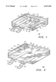
- FIG. 1 illustrates a cut-away isometric view of a first embodiment of an electronic component in accordance with the present invention
- FIG. 2 illustrates a cut-away isometric view of an alternative embodiment of the electronic component of FIG. 1;
- FIG. 3 illustrates an isometric view of a portion of a different embodiment of an electronic component in accordance with the present invention.
- FIG. 4 illustrates an isometric view of a portion of yet another embodiment of an electronic component in accordance with the present invention.
- FIG. 1 illustrates a cut-away isometric view of an electronic or semiconductor component 100.
- Component 100 generally includes, among other features, a device substrate 101, electrical interconnects or leads 110 and 120, a mounting or support substrate 130, and a packaging material 140.
- Substrate 101 is comprised of a semiconductor substrate such as silicon, gallium arsenide, or the like. At least one semiconductor device 104 is formed in a top surface of substrate 101 using semiconductor manufacturing techniques known in the art. In the preferred embodiment, device 104 is a single power transistor such as an insulated gate bipolar transistor (IGBT). Alternatively, a bipolar-complimentary-metal-oxide-semiconductor (BiCMOS) integrated circuit or the like could be formed in substrate 101.
- IGBT insulated gate bipolar transistor
- BiCMOS bipolar-complimentary-metal-oxide-semiconductor
- Electrode conductive layers 102 and 103 are formed over device 104 and supported by the top surface of substrate 101.
- Layer 102 has a hole in which layer 103 is located, and layers 102 and 103 can be coplanar with each other.
- Layers 102 and 103 are electrically coupled to different portions of device 104.
- layer 102 serves as a high current emitter electrode for device 104
- layer 103 serves as a lower current base electrode for device 104.
- Layers 102 and 103 can be formed by electroplating or otherwise depositing a metal layer over substrate 101 and then dividing the metal layer into two physically separated regions (i.e., layers 102 and 103) by an etching process. Alternatively, layers 102 and 103 can be sequentially, instead of simultaneously, formed over substrate 101.
- Substrate 101 is disposed over support substrate 130, which is larger than substrate 101.
- the front or top surface of substrate 101 faces away from substrate 130 while the back or bottom surface of substrate 101 is mounted on an electrically conductive mounting region 131 of substrate 130.
- region 131 is electrically coupled to the collector of device 104 by solder or another electrically conductive adhesive.
- Substrate 130 can be electrically insulative, and electrically conductive mounting region 131 can extend through substrate 130 to serve as an electrical lead at a backside surface of substrate 130.
- Lead 110 is electrically coupled to device 104 through electrically conductive layer 102.
- lead 110 has an electrical coupling portion 112 mounted on and supported by an electrical coupling portion or bonding or contact region of layer 102.
- Portion 112 is also referred to as an attachment portion.
- layer 102 itself is comprised of solder.
- a separate electrically conductive adhesive can be used to physically and electrically couple electrical coupling portion 112 to the bonding region of layer 102.
- the bonding region of layer 102 is the entire top surface of layer 102.
- a passivation layer (not shown) covers a portion of the top surface of substrate 101 and also covers an outer perimeter of layer 102, the bonding region of layer 102 is less than the entire top surface of layer 102 and is only a central portion of the top surface of layer 102.
- electrical coupling portion 112 is shaped to maximize a coupling surface area between the bonding region of layer 102 and electrical coupling portion 112 of lead 110. Maximizing the coupling surface area decreases the sheet resistance, which reduces the parasitic on-resistance of component 100.
- portion 112 covers at least seventy percent of the surface area of the bonding region of layer 102. In the preferred embodiment, portion 112 covers at least ninety percent of the surface area of the bonding region to reduce the parasitic on-resistance of component 100.
- Portion 112 preferably does not cover any portion of layer 103 to reduce the possibility of accidentally electrically shorting together layers 102 and 103.
- portion 112 promotes mechanical interlocking with an encapsulant, as explained in more detail hereinafter.
- Portion 112 is larger or wider than other portions of lead 110, including a distal end or portion 111 located at an opposite end of lead 110.
- the wider configuration of portion 112 improves or reduces the aforementioned parasitic on-resistance of component 100.
- Portion 112 has a plurality of protrusions, fingers, or ends 114 defining a plurality of slots or notches 115 therebetween.
- the specific configuration of ends 114 and notches 115 depicted in FIG. 1 is for illustration purposes only and is not intended to limit the scope of the present invention.
- ends 114 and notches 115 are at a perimeter of portion 112 and are adjacent to and overlie layer 102.
- Each of ends 114 have a surface substantially parallel to the bonding region of layer 102 in order to maximize the coupling surface area between the bonding region of layer 102 and lead 110.
- the presence of notches 115 over layer 102 reduces the reliability failures of component 100 caused by the thermal expansion differences between substrate 101 and lead 110.
- Portion 112 also has a through-hole 113 at its center wherein hole 113 extends entirely through portion 112 and wherein hole 113 exposes and provides access to layer 103.
- Hole 113 is preferably concentric with the hole of layer 102. Although not depicted in FIG. 1, hole 113 can also expose a central portion of layer 102.
- Lead 120 is inserted into hole 113 and is electrically coupled to device 104 though layer 103.
- lead 120 has an electrical coupling portion 122 mounted on and supported by an electrical coupling portion or bonding region of layer 103.
- the bonding regions of layers 102 and 103 are similar to each other, and the bonding region of layer 103 can be coupled to portion 122 of lead 120 in a manner similar to the coupling of the bonding region of layer 102 and portion 112 of lead 110.
- a distal portion 121 of lead 120 is at an opposite end from electrical coupling portion 122.
- Leads 110 and 120 are not electrically shorted together through layers 102 or 103 or through substrate 101 to permit proper electrical operation of device 104.
- Leads 110 and 120 can have a minimum cross-sectional area larger than that of a conventional wire bond to increase the current carrying capabilities of leads 110 and 120.
- Leads 110 and 120 can be comprised of copper, aluminum, gold, nickel-iron, or other malleable and electrically conductive material. Leads 110 and 120 can be formed by stamping, coining, or otherwise deforming a sheet of electrically conductive material into the shapes depicted in FIG. 1.
- Packaging material 140 covers or surrounds substrate 101, electrically conductive layers 102 and 103, portion 112 of lead 110, and portion 122 of lead 120.
- Material 140 can be a high pressure injection molded encapsulant, a glob top material, or the like.
- Substrate 101 supports a portion of material 140; portion 111 of lead 110 protrudes or extends out of material 140; and portion 121 of lead 120 protrudes or extends out of material 140.
- material 140 can fully surround substrate 130.
- electrically conductive region 131 extends through substrate 130, protrudes from the back surface of substrate 130, and is coplanar with material 140 at the backside of component 100 to provide an external electrical connection to device 104.
- material 140 can merely rest on top of substrate 130 while region 131 is coplanar with the back surface of substrate 130 to provide an external electrical connection to device 104.
- the perimeter of portion 112 of lead 110 has ends 114 and notches 115, which serve as a mold-locking feature by improving the mechanical interlocking between material 140 and lead 110.
- Ends 114 and notches 115 can be used in addition to conventional mold-locking features, which are not illustrated in FIG. 1 in order to simplify the explanation of component 100.
- Ends 114 and notches 115 maintain an orientation of lead 110 relative to substrates 101 and 130 because material 140 is disposed in notches 115 between ends 114.
- the specific size and configuration of notches 115 can be adjusted to improve the overall cosmetic appearance of packaging material 140.
- ends 114 and notches 115 extend beyond layer 102 and substrate 101 to form a gap between lead 110 and substrate 130 to enhance the mold-locking function of ends 114 and notches 115.
- electrical coupling portion 122 can have similar mold-locking features as electrical coupling portion 112.
- FIG. 2 illustrates a cut-away isometric view of an electronic component 200, which is an alternative embodiment of component 100 in FIG. 1.
- Component 200 has an electrical interconnect or lead 210, which is similar to lead 110 of component 100.
- Lead 210 has a distal portion 211 opposite an electrical coupling portion 212.
- Portion 212 has a through-hole 213 at a central portion and has protrusions, fingers, or ends 214 defining slots or notches 215 therebetween.
- Portion 212 of lead 210 is larger than portion 112 of lead 110.
- ends 214 and notches 215 extend beyond and do not overlie layer 102 or substrate 101. Therefore, portion 212 of lead 210 is larger than layer 102.
- Support substrate 230 is similar to substrate 130 of component 100, but substrate 230 is electrically conductive and serves as a third electrode for component 200. With a packaging material 240 resting entirely on top of substrate 230, component 200 can be a surface mount device wherein the bottom surfaces of distal portions 121 and 211 of leads 120 and 210, respectively, are coplanar with the bottom surface of substrate 230.
- the body or central region of leads 120 and 210 are disposed further away from substrate 230 than electrical coupling portions 122 and 212 of leads 120 and 210, respectively.
- ends 214 of portion 212 can be bent upwards and away from layer 102 and substrates 101 and 230 to provide a larger distance between the collector and emitter electrodes of component 200.
- the bent configuration of ends 214 can be similar to the bent configuration of the body or central region of leads 120 and 210.
- FIG. 3 illustrates an isometric view of a portion of an electronic component 300.
- Component 300 includes a substrate 301, a device 304, and electrically conductive layers 302 and 303, which are similar to substrates 101, device 104, and layers 102 and 103, respectively, of component 100 in FIG. 1.
- component 300 also includes an encapsulant and a support substrate similar to those described earlier for components 100 and 200.
- Component 300 also includes an electrical interconnect or lead 310 electrically coupled to device 304 through layer 302.
- Lead 310 has an electrical coupling portion 312 opposite a distal end 311.
- Portion 312 is shaped to maximize a coupling surface area between the bonding region of layer 302 and lead 310.
- Portion 312 has protrusions, fingers, or ends 314 defining slots or notches 315 therebetween.
- ends 314 and notches 315 depicted in FIG. 3 is for illustration purposes only and is not intended to limit the scope of the present invention. Notches 315 extend beyond substrate 301 to facilitate the disposal of encapsulant (not shown) around lead 310 and substrate 301 without entrapping air.
- a lead similar to lead 310 can be used to provide electrical coupling to layer 303.
- a wire bond or a lead similar to leads 110 or 120 of component 100 in FIG. 1 could also be used to provide electrical coupling to layer 303.
- FIG. 4 illustrates an isometric view of an electronic component 400.
- Component 400 includes a substrate 401, a device 404, and electrically conductive layers 402 and 403, which are similar to substrates 101, device 104, and layers 102 and 103, respectively, of component 100 in FIG. 1.
- component 400 also includes an encapsulant and a support substrate similar to those described earlier for components 100 and 200.
- Component 400 also has electrical interconnects or leads 410 and 420 electrically coupled to device 404 through layers 402 and 403, respectively.
- Leads 410 and 420 have electrical coupling portions 412 and 422, respectively, opposite distal portions 411 and 421, respectively.
- Portions 412 and 422 are shaped to maximize a coupling surface area between the bonding region of layer 402 and lead 410 and between the bonding region of layer 403 and lead 420.
- Lead 410 is a wire that can have a circular, oval, or other curved cross-section having a cross-sectional area to provide high current carrying capabilities.
- an oval cross-section of lead 410 provides the best manufacturability for the solder reflow process used to electrically and physically couple lead 410 to layer 402.
- An oval cross-section of lead 410 also minimizes the stress at the interface between lead 410 and an encapsulant (not shown in FIG. 4).
- lead 410 can also be a ribbon having a more rectangular cross-section.
- Lead 420 can be similar to lead 410, but can have a smaller cross-sectional area because of the lower current carrying requirements for lead 420.
- leads 410 and 420 are initially drawn from a spool of wire. Then, portions 412 and 422 are deformed or flattened to be larger or wider than the other portions of leads 410 and 420, respectively, as portrayed in FIG. 4. Portions 412 and 422 are deformed to extend radially from a central portion of leads 410 and 420, respectively, wherein body or central portions of leads 410 and 420 couple distal portions 411 and 421, respectively, to portions 412 and 422, respectively. The deforming process increases a coupling surface area between lead 410 and layer 402 and between lead 420 and layer 403.
- This deforming process can be accomplished by, among other processes, a cold-heading process, which is known in the non-semiconductor art and non-electronic component art of making nails and screws.
- a cold-heading process instead of a stamping or coining process
- little material if any is wasted or scrapped.
- the deformation process shapes portions 412 an 422 to each have at least one notch to improve the mold-locking characteristics of portions 412 and 422.
- portions 412 and 422 extend beyond layers 402 and 403, respectively, and even beyond substrate 401 as long as portions 412 and 422 do not electrically short together layers 402 and 403.
- portions 412 and 422 are electrically and physically coupled or attached to layers 402 and 403, respectively, by using solder or some other electrically conductive adhesive.
- the coupling or attaching process does not substantially deform or otherwise re-shape portions 412 and 422.
- the coupling or attaching process is substantially devoid of forming a eutectic or intermetallic joint, as typically formed in wire bonding applications.
- the electronic component presented herein has low parasitic on-resistance because of the increased coupling surface area between the electrical interconnects and the bonding pads of the semiconductor device.
- the electronic component presented herein also has higher current carrying capabilities because of the larger cross-sectional areas of the electrical interconnects.
- leads 110, 120, 210, 310, 410, and 420 are described to replace both wire bonds and leadframes, the leads described herein can also be used to merely replace wire bonds by electrically coupling a semiconductor device to a conventional leadframe.
- a lead similar to lead 110 could have portion 112 at both of its distal ends.
- leads 110, 210, 310, or 410 can be used in a rectifier or other two terminal device or in an integrated circuit.
Landscapes
- Structures For Mounting Electric Components On Printed Circuit Boards (AREA)
Abstract
Description
Claims (18)
Priority Applications (1)
| Application Number | Priority Date | Filing Date | Title |
|---|---|---|---|
| US09/033,188 US6147410A (en) | 1998-03-02 | 1998-03-02 | Electronic component and method of manufacture |
Applications Claiming Priority (1)
| Application Number | Priority Date | Filing Date | Title |
|---|---|---|---|
| US09/033,188 US6147410A (en) | 1998-03-02 | 1998-03-02 | Electronic component and method of manufacture |
Publications (1)
| Publication Number | Publication Date |
|---|---|
| US6147410A true US6147410A (en) | 2000-11-14 |
Family
ID=21868999
Family Applications (1)
| Application Number | Title | Priority Date | Filing Date |
|---|---|---|---|
| US09/033,188 Expired - Lifetime US6147410A (en) | 1998-03-02 | 1998-03-02 | Electronic component and method of manufacture |
Country Status (1)
| Country | Link |
|---|---|
| US (1) | US6147410A (en) |
Cited By (5)
| Publication number | Priority date | Publication date | Assignee | Title |
|---|---|---|---|---|
| EP1271648A1 (en) * | 2001-06-22 | 2003-01-02 | Siliconx (Taiwan) Ltd | Power semiconductor package and method for making the same |
| US20130323526A1 (en) * | 2012-05-29 | 2013-12-05 | Essence Solar Solutions Ltd. | Self aligning soldering |
| US10964628B2 (en) | 2019-02-21 | 2021-03-30 | Infineon Technologies Ag | Clip frame assembly, semiconductor package having a lead frame and a clip frame, and method of manufacture |
| EP3872848A1 (en) * | 2020-02-27 | 2021-09-01 | Littelfuse, Inc. | Metal tab for chip assembly |
| US11515244B2 (en) | 2019-02-21 | 2022-11-29 | Infineon Technologies Ag | Clip frame assembly, semiconductor package having a lead frame and a clip frame, and method of manufacture |
Citations (6)
| Publication number | Priority date | Publication date | Assignee | Title |
|---|---|---|---|---|
| US3061766A (en) * | 1955-12-07 | 1962-10-30 | Motorola Inc | Semiconductor device |
| US3153750A (en) * | 1958-10-14 | 1964-10-20 | Motorola Inc | Semiconductor device with two-piece self-jigging connectors |
| US5110761A (en) * | 1988-09-09 | 1992-05-05 | Motorola, Inc. | Formed top contact for non-flat semiconductor devices |
| US5218231A (en) * | 1989-08-30 | 1993-06-08 | Kabushiki Kaisha Toshiba | Mold-type semiconductor device |
| US5665996A (en) * | 1994-12-30 | 1997-09-09 | Siliconix Incorporated | Vertical power mosfet having thick metal layer to reduce distributed resistance |
| US5894170A (en) * | 1996-08-29 | 1999-04-13 | Nec Corporation | Wiring layer in semiconductor device |
-
1998
- 1998-03-02 US US09/033,188 patent/US6147410A/en not_active Expired - Lifetime
Patent Citations (6)
| Publication number | Priority date | Publication date | Assignee | Title |
|---|---|---|---|---|
| US3061766A (en) * | 1955-12-07 | 1962-10-30 | Motorola Inc | Semiconductor device |
| US3153750A (en) * | 1958-10-14 | 1964-10-20 | Motorola Inc | Semiconductor device with two-piece self-jigging connectors |
| US5110761A (en) * | 1988-09-09 | 1992-05-05 | Motorola, Inc. | Formed top contact for non-flat semiconductor devices |
| US5218231A (en) * | 1989-08-30 | 1993-06-08 | Kabushiki Kaisha Toshiba | Mold-type semiconductor device |
| US5665996A (en) * | 1994-12-30 | 1997-09-09 | Siliconix Incorporated | Vertical power mosfet having thick metal layer to reduce distributed resistance |
| US5894170A (en) * | 1996-08-29 | 1999-04-13 | Nec Corporation | Wiring layer in semiconductor device |
Cited By (10)
| Publication number | Priority date | Publication date | Assignee | Title |
|---|---|---|---|---|
| EP1271648A1 (en) * | 2001-06-22 | 2003-01-02 | Siliconx (Taiwan) Ltd | Power semiconductor package and method for making the same |
| US20130323526A1 (en) * | 2012-05-29 | 2013-12-05 | Essence Solar Solutions Ltd. | Self aligning soldering |
| US8900911B2 (en) | 2012-05-29 | 2014-12-02 | Essence Solar Solutions Ltd. | Frame holder |
| US9825194B2 (en) * | 2012-05-29 | 2017-11-21 | Essence Solar Solutions Ltd. | Self aligning soldering |
| US9917224B2 (en) | 2012-05-29 | 2018-03-13 | Essence Solar Solutions Ltd. | Photovoltaic module assembly |
| US10964628B2 (en) | 2019-02-21 | 2021-03-30 | Infineon Technologies Ag | Clip frame assembly, semiconductor package having a lead frame and a clip frame, and method of manufacture |
| US11515244B2 (en) | 2019-02-21 | 2022-11-29 | Infineon Technologies Ag | Clip frame assembly, semiconductor package having a lead frame and a clip frame, and method of manufacture |
| US12575429B2 (en) | 2019-02-21 | 2026-03-10 | Infineon Technologies Ag | Semiconductor package having a lead frame and a clip frame |
| EP3872848A1 (en) * | 2020-02-27 | 2021-09-01 | Littelfuse, Inc. | Metal tab for chip assembly |
| US11798868B2 (en) | 2020-02-27 | 2023-10-24 | Littelfuse, Inc. | Metal tab for chip assembly |
Similar Documents
| Publication | Publication Date | Title |
|---|---|---|
| US7443014B2 (en) | Electronic module and method of assembling the same | |
| JP3256636B2 (en) | Pressure contact type semiconductor device | |
| US6201186B1 (en) | Electronic component assembly and method of making the same | |
| EP0358077B1 (en) | Semiconductor device and method of forming it | |
| JP5492367B2 (en) | Package for gallium nitride semiconductor devices | |
| US5625226A (en) | Surface mount package with improved heat transfer | |
| US8343811B2 (en) | Semiconductor device | |
| US20070138648A1 (en) | Schottky Diode Device with Aluminum Pickup of Backside Cathode | |
| US5216279A (en) | Power semiconductor device suitable for automation of production | |
| JPH07123149B2 (en) | Semiconductor package | |
| US12519042B2 (en) | Methods for manufacturing a semiconductor package and a semiconductor module | |
| EP0418891B1 (en) | Moulded plastic power semiconductor device | |
| US5110761A (en) | Formed top contact for non-flat semiconductor devices | |
| US7274092B2 (en) | Semiconductor component and method of assembling the same | |
| US6147410A (en) | Electronic component and method of manufacture | |
| US6876067B2 (en) | Semiconductor device | |
| CN114050134B (en) | Semiconductor circuit with a high-voltage power supply | |
| JPH1098133A (en) | Semiconductor device and manufacturing method thereof | |
| JPH0645504A (en) | Semiconductor device | |
| EP2309538A2 (en) | Package for semiconductor devices | |
| US5473193A (en) | Package for parallel subelement semiconductor devices | |
| CN111987050A (en) | Semiconductor package with space-saving lead and die pad design | |
| CN118676085A (en) | Semiconductor devices | |
| JPH0513624A (en) | Semiconductor device | |
| KR20020004586A (en) | Semiconductor package |
Legal Events
| Date | Code | Title | Description |
|---|---|---|---|
| STCF | Information on status: patent grant |
Free format text: PATENTED CASE |
|
| FPAY | Fee payment |
Year of fee payment: 4 |
|
| AS | Assignment |
Owner name: FREESCALE SEMICONDUCTOR, INC., TEXAS Free format text: ASSIGNMENT OF ASSIGNORS INTEREST;ASSIGNOR:MOTOROLA, INC.;REEL/FRAME:015698/0657 Effective date: 20040404 Owner name: FREESCALE SEMICONDUCTOR, INC.,TEXAS Free format text: ASSIGNMENT OF ASSIGNORS INTEREST;ASSIGNOR:MOTOROLA, INC.;REEL/FRAME:015698/0657 Effective date: 20040404 |
|
| AS | Assignment |
Owner name: CITIBANK, N.A. AS COLLATERAL AGENT, NEW YORK Free format text: SECURITY AGREEMENT;ASSIGNORS:FREESCALE SEMICONDUCTOR, INC.;FREESCALE ACQUISITION CORPORATION;FREESCALE ACQUISITION HOLDINGS CORP.;AND OTHERS;REEL/FRAME:018855/0129 Effective date: 20061201 Owner name: CITIBANK, N.A. AS COLLATERAL AGENT,NEW YORK Free format text: SECURITY AGREEMENT;ASSIGNORS:FREESCALE SEMICONDUCTOR, INC.;FREESCALE ACQUISITION CORPORATION;FREESCALE ACQUISITION HOLDINGS CORP.;AND OTHERS;REEL/FRAME:018855/0129 Effective date: 20061201 |
|
| FPAY | Fee payment |
Year of fee payment: 8 |
|
| AS | Assignment |
Owner name: CITIBANK, N.A., AS COLLATERAL AGENT,NEW YORK Free format text: SECURITY AGREEMENT;ASSIGNOR:FREESCALE SEMICONDUCTOR, INC.;REEL/FRAME:024397/0001 Effective date: 20100413 Owner name: CITIBANK, N.A., AS COLLATERAL AGENT, NEW YORK Free format text: SECURITY AGREEMENT;ASSIGNOR:FREESCALE SEMICONDUCTOR, INC.;REEL/FRAME:024397/0001 Effective date: 20100413 |
|
| FPAY | Fee payment |
Year of fee payment: 12 |
|
| AS | Assignment |
Owner name: CITIBANK, N.A., AS NOTES COLLATERAL AGENT, NEW YORK Free format text: SECURITY AGREEMENT;ASSIGNOR:FREESCALE SEMICONDUCTOR, INC.;REEL/FRAME:030633/0424 Effective date: 20130521 Owner name: CITIBANK, N.A., AS NOTES COLLATERAL AGENT, NEW YOR Free format text: SECURITY AGREEMENT;ASSIGNOR:FREESCALE SEMICONDUCTOR, INC.;REEL/FRAME:030633/0424 Effective date: 20130521 |
|
| AS | Assignment |
Owner name: CITIBANK, N.A., AS NOTES COLLATERAL AGENT, NEW YORK Free format text: SECURITY AGREEMENT;ASSIGNOR:FREESCALE SEMICONDUCTOR, INC.;REEL/FRAME:031591/0266 Effective date: 20131101 Owner name: CITIBANK, N.A., AS NOTES COLLATERAL AGENT, NEW YOR Free format text: SECURITY AGREEMENT;ASSIGNOR:FREESCALE SEMICONDUCTOR, INC.;REEL/FRAME:031591/0266 Effective date: 20131101 |
|
| AS | Assignment |
Owner name: FREESCALE SEMICONDUCTOR, INC., TEXAS Free format text: PATENT RELEASE;ASSIGNOR:CITIBANK, N.A., AS COLLATERAL AGENT;REEL/FRAME:037354/0225 Effective date: 20151207 Owner name: FREESCALE SEMICONDUCTOR, INC., TEXAS Free format text: PATENT RELEASE;ASSIGNOR:CITIBANK, N.A., AS COLLATERAL AGENT;REEL/FRAME:037356/0143 Effective date: 20151207 Owner name: FREESCALE SEMICONDUCTOR, INC., TEXAS Free format text: PATENT RELEASE;ASSIGNOR:CITIBANK, N.A., AS COLLATERAL AGENT;REEL/FRAME:037356/0553 Effective date: 20151207 |
|
| AS | Assignment |
Owner name: MORGAN STANLEY SENIOR FUNDING, INC., MARYLAND Free format text: ASSIGNMENT AND ASSUMPTION OF SECURITY INTEREST IN PATENTS;ASSIGNOR:CITIBANK, N.A.;REEL/FRAME:037486/0517 Effective date: 20151207 |
|
| AS | Assignment |
Owner name: MORGAN STANLEY SENIOR FUNDING, INC., MARYLAND Free format text: ASSIGNMENT AND ASSUMPTION OF SECURITY INTEREST IN PATENTS;ASSIGNOR:CITIBANK, N.A.;REEL/FRAME:037518/0292 Effective date: 20151207 |
|
| AS | Assignment |
Owner name: MORGAN STANLEY SENIOR FUNDING, INC., MARYLAND Free format text: SUPPLEMENT TO THE SECURITY AGREEMENT;ASSIGNOR:FREESCALE SEMICONDUCTOR, INC.;REEL/FRAME:039138/0001 Effective date: 20160525 |
|
| AS | Assignment |
Owner name: NXP, B.V., F/K/A FREESCALE SEMICONDUCTOR, INC., NETHERLANDS Free format text: RELEASE BY SECURED PARTY;ASSIGNOR:MORGAN STANLEY SENIOR FUNDING, INC.;REEL/FRAME:040925/0001 Effective date: 20160912 Owner name: NXP, B.V., F/K/A FREESCALE SEMICONDUCTOR, INC., NE Free format text: RELEASE BY SECURED PARTY;ASSIGNOR:MORGAN STANLEY SENIOR FUNDING, INC.;REEL/FRAME:040925/0001 Effective date: 20160912 |
|
| AS | Assignment |
Owner name: NXP B.V., NETHERLANDS Free format text: RELEASE BY SECURED PARTY;ASSIGNOR:MORGAN STANLEY SENIOR FUNDING, INC.;REEL/FRAME:040928/0001 Effective date: 20160622 |
|
| AS | Assignment |
Owner name: NXP USA, INC., TEXAS Free format text: CHANGE OF NAME;ASSIGNOR:FREESCALE SEMICONDUCTOR, INC.;REEL/FRAME:040652/0241 Effective date: 20161107 Owner name: NXP USA, INC., TEXAS Free format text: MERGER;ASSIGNOR:FREESCALE SEMICONDUCTOR, INC.;REEL/FRAME:040652/0241 Effective date: 20161107 |
|
| AS | Assignment |
Owner name: NXP USA, INC., TEXAS Free format text: CORRECTIVE ASSIGNMENT TO CORRECT THE NATURE OF CONVEYANCE PREVIOUSLY RECORDED AT REEL: 040652 FRAME: 0241. ASSIGNOR(S) HEREBY CONFIRMS THE MERGER AND CHANGE OF NAME;ASSIGNOR:FREESCALE SEMICONDUCTOR, INC.;REEL/FRAME:041260/0850 Effective date: 20161107 |
|
| AS | Assignment |
Owner name: MORGAN STANLEY SENIOR FUNDING, INC., MARYLAND Free format text: CORRECTIVE ASSIGNMENT TO CORRECT THE REMOVE PATENTS 8108266 AND 8062324 AND REPLACE THEM WITH 6108266 AND 8060324 PREVIOUSLY RECORDED ON REEL 037518 FRAME 0292. ASSIGNOR(S) HEREBY CONFIRMS THE ASSIGNMENT AND ASSUMPTION OF SECURITY INTEREST IN PATENTS;ASSIGNOR:CITIBANK, N.A.;REEL/FRAME:041703/0536 Effective date: 20151207 |
|
| AS | Assignment |
Owner name: SHENZHEN XINGUODU TECHNOLOGY CO., LTD., CHINA Free format text: CORRECTIVE ASSIGNMENT TO CORRECT THE TO CORRECT THE APPLICATION NO. FROM 13,883,290 TO 13,833,290 PREVIOUSLY RECORDED ON REEL 041703 FRAME 0536. ASSIGNOR(S) HEREBY CONFIRMS THE THE ASSIGNMENT AND ASSUMPTION OF SECURITYINTEREST IN PATENTS.;ASSIGNOR:MORGAN STANLEY SENIOR FUNDING, INC.;REEL/FRAME:048734/0001 Effective date: 20190217 Owner name: SHENZHEN XINGUODU TECHNOLOGY CO., LTD., CHINA Free format text: CORRECTIVE ASSIGNMENT TO CORRECT THE TO CORRECT THE APPLICATION NO. FROM 13,883,290 TO 13,833,290 PREVIOUSLY RECORDED ON REEL 041703 FRAME 0536. ASSIGNOR(S) HEREBY CONFIRMS THE THE ASSIGNMENT AND ASSUMPTION OF SECURITY INTEREST IN PATENTS.;ASSIGNOR:MORGAN STANLEY SENIOR FUNDING, INC.;REEL/FRAME:048734/0001 Effective date: 20190217 |
|
| AS | Assignment |
Owner name: NXP B.V., NETHERLANDS Free format text: RELEASE BY SECURED PARTY;ASSIGNOR:MORGAN STANLEY SENIOR FUNDING, INC.;REEL/FRAME:050744/0097 Effective date: 20190903 |
|
| AS | Assignment |
Owner name: MORGAN STANLEY SENIOR FUNDING, INC., MARYLAND Free format text: CORRECTIVE ASSIGNMENT TO CORRECT THE REMOVE APPLICATION11759915 AND REPLACE IT WITH APPLICATION 11759935 PREVIOUSLY RECORDED ON REEL 037486 FRAME 0517. ASSIGNOR(S) HEREBY CONFIRMS THE ASSIGNMENT AND ASSUMPTION OF SECURITYINTEREST IN PATENTS;ASSIGNOR:CITIBANK, N.A.;REEL/FRAME:053547/0421 Effective date: 20151207 Owner name: MORGAN STANLEY SENIOR FUNDING, INC., MARYLAND Free format text: CORRECTIVE ASSIGNMENT TO CORRECT THE REMOVE APPLICATION 11759915 AND REPLACE IT WITH APPLICATION 11759935 PREVIOUSLY RECORDED ON REEL 037486 FRAME 0517. ASSIGNOR(S) HEREBY CONFIRMS THE ASSIGNMENT AND ASSUMPTION OF SECURITY INTEREST IN PATENTS;ASSIGNOR:CITIBANK, N.A.;REEL/FRAME:053547/0421 Effective date: 20151207 |
|
| AS | Assignment |
Owner name: NXP B.V., NETHERLANDS Free format text: CORRECTIVE ASSIGNMENT TO CORRECT THE REMOVEAPPLICATION 11759915 AND REPLACE IT WITH APPLICATION11759935 PREVIOUSLY RECORDED ON REEL 040928 FRAME 0001. ASSIGNOR(S) HEREBY CONFIRMS THE RELEASE OF SECURITYINTEREST;ASSIGNOR:MORGAN STANLEY SENIOR FUNDING, INC.;REEL/FRAME:052915/0001 Effective date: 20160622 Owner name: NXP B.V., NETHERLANDS Free format text: CORRECTIVE ASSIGNMENT TO CORRECT THE REMOVE APPLICATION 11759915 AND REPLACE IT WITH APPLICATION 11759935 PREVIOUSLY RECORDED ON REEL 040928 FRAME 0001. ASSIGNOR(S) HEREBY CONFIRMS THE RELEASE OF SECURITY INTEREST;ASSIGNOR:MORGAN STANLEY SENIOR FUNDING, INC.;REEL/FRAME:052915/0001 Effective date: 20160622 |
|
| AS | Assignment |
Owner name: NXP, B.V. F/K/A FREESCALE SEMICONDUCTOR, INC., NETHERLANDS Free format text: CORRECTIVE ASSIGNMENT TO CORRECT THE REMOVEAPPLICATION 11759915 AND REPLACE IT WITH APPLICATION11759935 PREVIOUSLY RECORDED ON REEL 040925 FRAME 0001. ASSIGNOR(S) HEREBY CONFIRMS THE RELEASE OF SECURITYINTEREST;ASSIGNOR:MORGAN STANLEY SENIOR FUNDING, INC.;REEL/FRAME:052917/0001 Effective date: 20160912 Owner name: NXP, B.V. F/K/A FREESCALE SEMICONDUCTOR, INC., NETHERLANDS Free format text: CORRECTIVE ASSIGNMENT TO CORRECT THE REMOVE APPLICATION 11759915 AND REPLACE IT WITH APPLICATION 11759935 PREVIOUSLY RECORDED ON REEL 040925 FRAME 0001. ASSIGNOR(S) HEREBY CONFIRMS THE RELEASE OF SECURITY INTEREST;ASSIGNOR:MORGAN STANLEY SENIOR FUNDING, INC.;REEL/FRAME:052917/0001 Effective date: 20160912 |