US6147370A - Field effect transistor with first and second drain electrodes - Google Patents
Field effect transistor with first and second drain electrodes Download PDFInfo
- Publication number
- US6147370A US6147370A US08/933,836 US93383697A US6147370A US 6147370 A US6147370 A US 6147370A US 93383697 A US93383697 A US 93383697A US 6147370 A US6147370 A US 6147370A
- Authority
- US
- United States
- Prior art keywords
- semiconductor layer
- drain
- field effect
- effect transistor
- layer
- Prior art date
- Legal status (The legal status is an assumption and is not a legal conclusion. Google has not performed a legal analysis and makes no representation as to the accuracy of the status listed.)
- Expired - Lifetime
Links
Images


Classifications
-
- H—ELECTRICITY
- H10—SEMICONDUCTOR DEVICES; ELECTRIC SOLID-STATE DEVICES NOT OTHERWISE PROVIDED FOR
- H10D—INORGANIC ELECTRIC SEMICONDUCTOR DEVICES
- H10D30/00—Field-effect transistors [FET]
- H10D30/01—Manufacture or treatment
- H10D30/015—Manufacture or treatment of FETs having heterojunction interface channels or heterojunction gate electrodes, e.g. HEMT
-
- H—ELECTRICITY
- H01—ELECTRIC ELEMENTS
- H01L—SEMICONDUCTOR DEVICES NOT COVERED BY CLASS H10
- H01L21/00—Processes or apparatus adapted for the manufacture or treatment of semiconductor or solid state devices or of parts thereof
- H01L21/02—Manufacture or treatment of semiconductor devices or of parts thereof
- H01L21/04—Manufacture or treatment of semiconductor devices or of parts thereof the devices having potential barriers, e.g. a PN junction, depletion layer or carrier concentration layer
- H01L21/18—Manufacture or treatment of semiconductor devices or of parts thereof the devices having potential barriers, e.g. a PN junction, depletion layer or carrier concentration layer the devices having semiconductor bodies comprising elements of Group IV of the Periodic Table or AIIIBV compounds with or without impurities, e.g. doping materials
- H01L21/28—Manufacture of electrodes on semiconductor bodies using processes or apparatus not provided for in groups H01L21/20 - H01L21/268
- H01L21/283—Deposition of conductive or insulating materials for electrodes conducting electric current
- H01L21/285—Deposition of conductive or insulating materials for electrodes conducting electric current from a gas or vapour, e.g. condensation
- H01L21/28506—Deposition of conductive or insulating materials for electrodes conducting electric current from a gas or vapour, e.g. condensation of conductive layers
- H01L21/28575—Deposition of conductive or insulating materials for electrodes conducting electric current from a gas or vapour, e.g. condensation of conductive layers on semiconductor bodies comprising AIIIBV compounds
- H01L21/28587—Deposition of conductive or insulating materials for electrodes conducting electric current from a gas or vapour, e.g. condensation of conductive layers on semiconductor bodies comprising AIIIBV compounds characterised by the sectional shape, e.g. T, inverted T
-
- H—ELECTRICITY
- H10—SEMICONDUCTOR DEVICES; ELECTRIC SOLID-STATE DEVICES NOT OTHERWISE PROVIDED FOR
- H10D—INORGANIC ELECTRIC SEMICONDUCTOR DEVICES
- H10D30/00—Field-effect transistors [FET]
- H10D30/40—FETs having zero-dimensional [0D], one-dimensional [1D] or two-dimensional [2D] charge carrier gas channels
- H10D30/47—FETs having zero-dimensional [0D], one-dimensional [1D] or two-dimensional [2D] charge carrier gas channels having 2D charge carrier gas channels, e.g. nanoribbon FETs or high electron mobility transistors [HEMT]
- H10D30/471—High electron mobility transistors [HEMT] or high hole mobility transistors [HHMT]
- H10D30/472—High electron mobility transistors [HEMT] or high hole mobility transistors [HHMT] having lower bandgap active layer formed on top of wider bandgap layer, e.g. inverted HEMT
-
- H—ELECTRICITY
- H10—SEMICONDUCTOR DEVICES; ELECTRIC SOLID-STATE DEVICES NOT OTHERWISE PROVIDED FOR
- H10D—INORGANIC ELECTRIC SEMICONDUCTOR DEVICES
- H10D62/00—Semiconductor bodies, or regions thereof, of devices having potential barriers
- H10D62/10—Shapes, relative sizes or dispositions of the regions of the semiconductor bodies; Shapes of the semiconductor bodies
- H10D62/13—Semiconductor regions connected to electrodes carrying current to be rectified, amplified or switched, e.g. source or drain regions
- H10D62/149—Source or drain regions of field-effect devices
- H10D62/161—Source or drain regions of field-effect devices of FETs having Schottky gates
Definitions
- the present invention relates to a compound semiconductor field effect transistor with an enhanced drain current-voltage characteristics.
- FIG. 1 is a diagrammatic representation showing a conventional field effect transistor of a gallium arsenide schottky barrier type having a typical n-type conductive layer (GaAs MESFET).
- GaAs MESFET gallium arsenide schottky barrier type having a typical n-type conductive layer
- a schottky gate electrode 6 is formed, and on the n-layer 4 outside the recess, an ohmic source electrode 7 and a drain electrode 8 are formed.
- a layer of Au 10 is formed, and a rear-side electrode is grounded.
- An object of the present invention is to provide a FET difficult to destroy or deteriorate by inhibiting a drain current from being concentrated on the ends of a recess.
- a drain electrode is provided also on a rear side of a substrate. Specifically, by letting the drain current flow also from the rear side, the concentration of the current on the recess ends can be controlled.
- the drain electrode is formed on the rear side, as the substrate an n-type layer is used, and on the substrate, a low-concentration n-layer, a p-layer or an undoped GaAs layer (i-layer) is formed. If necessary, further on the layers, an AlGaAs layer is interposed having a broader band gap than the GaAs layer. On the layers, a MESFET having a usual n-type conductivity is formed. The aforementioned low-concentration n-layer, the p-layer, the i-layer or the AlGaAs layer prevents current from flowing between a source electrode on a surface side and the drain electrode on a rear side.
- the drain current can be controlled by the potential of a gate.
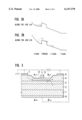
- FIG. 1 is a cross-sectional view of a GaAsFET having a conventional structure.
- FIG. 2A shows a conductive band between line A--A in FIG. 3, and FIG. 2B shows a conductive band between line B--B in FIG. 3.
- FIG. 3 is a cross-sectional view of a GaAsFET embodying the present invention.
- FIGS. 4A, 4B and 4C are cross-sectional views showing a manufacture process of the GaAsFET shown in FIG. 3 embodying the invention.
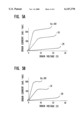
- FIG. 5A shows drain current-voltage characteristics of the FET according to the invention
- FIG. 5B shows drain current-voltage characteristics of a conventional FET.
- FIG. 6 is a cross-sectional view showing another embodiment of the GaAsFET according to the invention.
- FIG. 7 is a cross-sectional view showing further embodiment of the GaAsFET according to the invention.
- FIG. 8 is a cross-sectional view showing still further embodiment of the GaAsFET according to the invention.
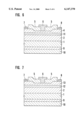
- FIG. 3 shows a cross section of GaAsFET of the invention, the manufacture of which will now be described in the following referring to FIGS. 4A, 4B and 4C.
- a resist layer is patterned, and the n-GaAs layer 4 in the vicinity of a gate region is etched by 0.15 ⁇ m using a solution of H 2 SO 4 +H 2 O 2 +H 2 O, to form a structure of recess.
- a SiO 2 film 5 is grown to 0.5 ⁇ m in a plasma CVD method.
- SiO 2 is etched or removed with HF from a region in which source and drain electrodes are to be formed, then 0.15 ⁇ m of AuGe and 0.04 ⁇ m of Ni are formed in a vacuum evaporation method. After removing the resist, thermal treatment is made at 400° C. for one minute, causing reaction of AuGe and Ni with GaAs, to form an ohmic source electrode 7 and a drain electrode 8.
- a drain voltage at which a drain current is rapidly increased i.e. a drain breakdown voltage characteristics was about 10V
- the breakdown voltage characteristics of nearly 20V was obtained.
- the breakdown voltage characteristics can be largely enhanced.
- FIG. 6 shows another embodiment of the invention, in which, different from the FET of FIG. 3, instead of the i-AlGaAs layer 3, a p-GaAs layer 11 is inserted under the n-GaAs layer 4.
- the p-GaAs layer 11 is constituted to have a concentration of 1 ⁇ 10 18 cm -3 and a thickness of 0.05 ⁇ m.
- the enhancement in the breakdown voltage characteristics can be achieved in the same manner as afore-mentioned.
- the other constitution is the same as in FIG. 3, therefore further description is omitted.
- FIG. 7 shows further embodiment of the invention.
- an i-In x Ga 1-x As layer 12 having X of nearly 0.2 and a thickness of 0.015 ⁇ m, and an n-AlGaAs layer 13 having a concentration of about 2 ⁇ 10 18 cm -3 and a thickness of 0.04 ⁇ m under the gate are formed.
- This structure is a so-called HEMT structure. Also in this case, the drain current-voltage characteristics can be improved. Since the other structure is the same as in FIG. 3, further description is omitted.
- FIG. 8 shows further embodiment of the invention.
- an n + GaAs layer 14 is formed on a surface drain region.
- the n + GaAs layer 14 permits electrons to easily flow toward a drain electrode 10 on the rear side, and can relax the concentration of electric field on recess ends. Since the other structure is the same as in FIG. 3, description is omitted.
- the drain resistant pressure can be enhanced.
Landscapes
- Engineering & Computer Science (AREA)
- Physics & Mathematics (AREA)
- Condensed Matter Physics & Semiconductors (AREA)
- General Physics & Mathematics (AREA)
- Manufacturing & Machinery (AREA)
- Computer Hardware Design (AREA)
- Microelectronics & Electronic Packaging (AREA)
- Power Engineering (AREA)
- Junction Field-Effect Transistors (AREA)
- Electrodes Of Semiconductors (AREA)
Abstract
Description
Claims (5)
Applications Claiming Priority (2)
| Application Number | Priority Date | Filing Date | Title |
|---|---|---|---|
| JP8-250169 | 1996-09-20 | ||
| JP08250169A JP3077599B2 (en) | 1996-09-20 | 1996-09-20 | Field effect transistor |
Publications (1)
| Publication Number | Publication Date |
|---|---|
| US6147370A true US6147370A (en) | 2000-11-14 |
Family
ID=17203854
Family Applications (1)
| Application Number | Title | Priority Date | Filing Date |
|---|---|---|---|
| US08/933,836 Expired - Lifetime US6147370A (en) | 1996-09-20 | 1997-09-19 | Field effect transistor with first and second drain electrodes |
Country Status (2)
| Country | Link |
|---|---|
| US (1) | US6147370A (en) |
| JP (1) | JP3077599B2 (en) |
Cited By (4)
| Publication number | Priority date | Publication date | Assignee | Title |
|---|---|---|---|---|
| US6333523B1 (en) * | 1998-10-30 | 2001-12-25 | Sumitomo Electric Industries, Ltd. | Field-effect transistor |
| US20050001235A1 (en) * | 2003-05-15 | 2005-01-06 | Tomohiro Murata | Semiconductor device |
| US20090154210A1 (en) * | 2004-12-09 | 2009-06-18 | Sumitomo Electric Industries, Ltd. | Bidirectional field-effect transistor and matrix converter |
| US20090218598A1 (en) * | 2006-03-08 | 2009-09-03 | Sanken Electric Co., Ltd. | Warp-free semiconductor wafer, and devices using the same |
Citations (4)
| Publication number | Priority date | Publication date | Assignee | Title |
|---|---|---|---|---|
| US4636823A (en) * | 1984-06-05 | 1987-01-13 | California Institute Of Technology | Vertical Schottky barrier gate field-effect transistor in GaAs/GaAlAs |
| US5060030A (en) * | 1990-07-18 | 1991-10-22 | Raytheon Company | Pseudomorphic HEMT having strained compensation layer |
| US5140386A (en) * | 1991-05-09 | 1992-08-18 | Raytheon Company | High electron mobility transistor |
| JPH04237136A (en) * | 1991-01-22 | 1992-08-25 | Nec Corp | Gallium arsenic field effect transistor |
-
1996
- 1996-09-20 JP JP08250169A patent/JP3077599B2/en not_active Expired - Fee Related
-
1997
- 1997-09-19 US US08/933,836 patent/US6147370A/en not_active Expired - Lifetime
Patent Citations (4)
| Publication number | Priority date | Publication date | Assignee | Title |
|---|---|---|---|---|
| US4636823A (en) * | 1984-06-05 | 1987-01-13 | California Institute Of Technology | Vertical Schottky barrier gate field-effect transistor in GaAs/GaAlAs |
| US5060030A (en) * | 1990-07-18 | 1991-10-22 | Raytheon Company | Pseudomorphic HEMT having strained compensation layer |
| JPH04237136A (en) * | 1991-01-22 | 1992-08-25 | Nec Corp | Gallium arsenic field effect transistor |
| US5140386A (en) * | 1991-05-09 | 1992-08-18 | Raytheon Company | High electron mobility transistor |
Non-Patent Citations (3)
| Title |
|---|
| English language translation of Japanese Office Action dated Jul. 28, Hei 10. * |
| R. Yamamoto, et al., "Light Emission and Burnout Characteristics of GaAs Power MESFET's", IEEE Transactions of Electron Devices, vol. ED-25, No. 6, Jun. 1978, pp. 567-573. |
| R. Yamamoto, et al., Light Emission and Burnout Characteristics of GaAs Power MESFET s , IEEE Transactions of Electron Devices, vol. ED 25, No. 6, Jun. 1978, pp. 567 573. * |
Cited By (7)
| Publication number | Priority date | Publication date | Assignee | Title |
|---|---|---|---|---|
| US6333523B1 (en) * | 1998-10-30 | 2001-12-25 | Sumitomo Electric Industries, Ltd. | Field-effect transistor |
| US20050001235A1 (en) * | 2003-05-15 | 2005-01-06 | Tomohiro Murata | Semiconductor device |
| US20060289894A1 (en) * | 2003-05-15 | 2006-12-28 | Matsushita Electric Industrial Co., Ltd. | Semiconductor device |
| US7339207B2 (en) * | 2003-05-15 | 2008-03-04 | Matsushita Electric Industrial Co., Ltd. | Semiconductor device including a group III-V nitride semiconductor |
| US20090154210A1 (en) * | 2004-12-09 | 2009-06-18 | Sumitomo Electric Industries, Ltd. | Bidirectional field-effect transistor and matrix converter |
| US20090218598A1 (en) * | 2006-03-08 | 2009-09-03 | Sanken Electric Co., Ltd. | Warp-free semiconductor wafer, and devices using the same |
| US7982242B2 (en) * | 2006-03-08 | 2011-07-19 | Sanken Electric Co., Ltd. | Warp-free semiconductor wafer, and devices using the same |
Also Published As
| Publication number | Publication date |
|---|---|
| JPH1098057A (en) | 1998-04-14 |
| JP3077599B2 (en) | 2000-08-14 |
Similar Documents
| Publication | Publication Date | Title |
|---|---|---|
| US7291872B2 (en) | Semiconductor device and method for fabricating the same | |
| JP4705412B2 (en) | Field effect transistor and manufacturing method thereof | |
| US4984036A (en) | Field effect transistor with multiple grooves | |
| US6908799B2 (en) | High electron mobility transistor and method of manufacturing the same | |
| US20070164326A1 (en) | Field effect transistor | |
| EP0551110B1 (en) | Compound semiconductor devices | |
| US8710548B2 (en) | Semiconductor device and method for manufacturing the same | |
| WO2011013306A1 (en) | Semiconductor device | |
| JP3294411B2 (en) | Method for manufacturing semiconductor device | |
| US5610410A (en) | III-V compound semiconductor device with Schottky electrode of increased barrier height | |
| JP4182376B2 (en) | Semiconductor device | |
| TWI404204B (en) | Single-wafer integrated circuit with enhanced/depleted field effect transistor and RF/microwave/millimeter wave field effect transistor | |
| JP2010016089A (en) | Field effect transistor, method of manufacturing the same, and semiconductor device | |
| JP4064800B2 (en) | Heterojunction compound semiconductor field effect transistor and method of manufacturing the same | |
| US6147370A (en) | Field effect transistor with first and second drain electrodes | |
| US20240347603A1 (en) | Nitride semiconductor device and method for manufacturing the same | |
| US7498223B2 (en) | Semiconductor devices having improved field plates | |
| US5231040A (en) | Method of making a field effect transistor | |
| US6458675B1 (en) | Semiconductor device having a plasma-processed layer and method of manufacturing the same | |
| US5523593A (en) | Compound semiconductor integrated circuit and optical regenerative repeater using the same | |
| US5837570A (en) | Heterostructure semiconductor device and method of fabricating same | |
| JP3588988B2 (en) | Semiconductor device | |
| US20240387415A1 (en) | Nitride semiconductor device and manufacturing method therefor | |
| US20060175631A1 (en) | Monolithic integrated circuit having enhanced breakdown voltage | |
| JP3347837B2 (en) | Compound semiconductor field effect transistor |
Legal Events
| Date | Code | Title | Description |
|---|---|---|---|
| AS | Assignment |
Owner name: NEC CORPORATION, JAPAN Free format text: ASSIGNMENT OF ASSIGNORS INTEREST;ASSIGNOR:KANAMORI, MIKIO;REEL/FRAME:008828/0369 Effective date: 19970916 |
|
| STCF | Information on status: patent grant |
Free format text: PATENTED CASE |
|
| FEPP | Fee payment procedure |
Free format text: PAYOR NUMBER ASSIGNED (ORIGINAL EVENT CODE: ASPN); ENTITY STATUS OF PATENT OWNER: LARGE ENTITY |
|
| AS | Assignment |
Owner name: NEC COMPOUND SEMICONDUCTOR DEVICES, LTD., JAPAN Free format text: ASSIGNMENT OF ASSIGNORS INTEREST;ASSIGNOR:NEC CORPORATION;REEL/FRAME:013496/0038 Effective date: 20020919 |
|
| FPAY | Fee payment |
Year of fee payment: 4 |
|
| AS | Assignment |
Owner name: NEC ELECTRONICS CORPORATION, JAPAN Free format text: ASSIGNMENT OF ASSIGNORS INTEREST;ASSIGNOR:NEC COMPOUND SEMICONDUCTOR DEVICES, LTD.;REEL/FRAME:017422/0528 Effective date: 20060315 |
|
| FPAY | Fee payment |
Year of fee payment: 8 |
|
| AS | Assignment |
Owner name: RENESAS ELECTRONICS CORPORATION, JAPAN Free format text: CHANGE OF NAME;ASSIGNOR:NEC ELECTRONICS CORPORATION;REEL/FRAME:025183/0589 Effective date: 20100401 |
|
| FPAY | Fee payment |
Year of fee payment: 12 |