US6144569A - System and method for recovering from a power supply interruption - Google Patents
System and method for recovering from a power supply interruption Download PDFInfo
- Publication number
- US6144569A US6144569A US09/514,800 US51480000A US6144569A US 6144569 A US6144569 A US 6144569A US 51480000 A US51480000 A US 51480000A US 6144569 A US6144569 A US 6144569A
- Authority
- US
- United States
- Prior art keywords
- voltage level
- level
- electronic apparatus
- state
- circuit
- Prior art date
- Legal status (The legal status is an assumption and is not a legal conclusion. Google has not performed a legal analysis and makes no representation as to the accuracy of the status listed.)
- Expired - Lifetime
Links
- 238000000034 method Methods 0.000 title claims description 27
- 238000011084 recovery Methods 0.000 claims abstract description 18
- 230000004044 response Effects 0.000 claims abstract description 14
- 238000012544 monitoring process Methods 0.000 claims abstract description 12
- 238000001514 detection method Methods 0.000 claims abstract description 11
- 239000013643 reference control Substances 0.000 claims abstract description 9
- 230000001419 dependent effect Effects 0.000 claims abstract description 5
- 230000003247 decreasing effect Effects 0.000 claims 1
- 230000001413 cellular effect Effects 0.000 description 55
- 230000007704 transition Effects 0.000 description 10
- 238000010586 diagram Methods 0.000 description 8
- 238000000825 ultraviolet detection Methods 0.000 description 6
- 230000006870 function Effects 0.000 description 5
- 230000007423 decrease Effects 0.000 description 2
- 230000005540 biological transmission Effects 0.000 description 1
- 230000002950 deficient Effects 0.000 description 1
- 230000001934 delay Effects 0.000 description 1
- 230000002939 deleterious effect Effects 0.000 description 1
- 238000013461 design Methods 0.000 description 1
- 230000000694 effects Effects 0.000 description 1
- 230000000977 initiatory effect Effects 0.000 description 1
- 238000012423 maintenance Methods 0.000 description 1
- 238000005259 measurement Methods 0.000 description 1
- 230000007246 mechanism Effects 0.000 description 1
- 230000008569 process Effects 0.000 description 1
- 230000001105 regulatory effect Effects 0.000 description 1
- 230000008439 repair process Effects 0.000 description 1
Images
Classifications
-
- G—PHYSICS
- G06—COMPUTING; CALCULATING OR COUNTING
- G06F—ELECTRIC DIGITAL DATA PROCESSING
- G06F1/00—Details not covered by groups G06F3/00 - G06F13/00 and G06F21/00
- G06F1/26—Power supply means, e.g. regulation thereof
- G06F1/30—Means for acting in the event of power-supply failure or interruption, e.g. power-supply fluctuations
-
- H—ELECTRICITY
- H04—ELECTRIC COMMUNICATION TECHNIQUE
- H04B—TRANSMISSION
- H04B1/00—Details of transmission systems, not covered by a single one of groups H04B3/00 - H04B13/00; Details of transmission systems not characterised by the medium used for transmission
- H04B1/06—Receivers
- H04B1/16—Circuits
- H04B1/1607—Supply circuits
Definitions
- This invention relates, in general to a system and method for power failure detection and recovery and, more particularly, to a method and system providing for the recovery of an electronic apparatus such as a cellular telephone in the event of a power supply disconnection.
- a momentary interruption in the power supplied by a power supply can cause deleterious effects when the power is restored.
- some electronic apparatus fails to restart properly, or fails to return to the pre-interruption state after the power supply is restored. This is especially true, for example, in an electronic apparatus that includes and requires precise reference supplies, such as reference voltages and reference currents.
- battery operated portable cellular telephones can experience an interruption in service if the battery power supply is momentarily disconnected from the telephone.
- a momentary interruption in the power supply can occur, for example, if a cellular phone that is turned on and is in the standby mode is accidentally dropped causing a momentary disconnection of the battery from the telephone.
- a momentary battery disconnect can occur if the cellular telephone is thrust into a pocket, purse, briefcase, belt holder, or the like.
- the voltage level within the cellular telephone drops, with the rate of drop largely dependent upon the capacitive loading and hence the time constant of the internal circuitry. If the power is restored before the internal voltage falls to a value below which the internal references fail to operate, the cellular telephone will return to its operating state without further interruption of service. Similarly, if the battery interruption is terminated after the internal voltages have dropped to a level below the power on reset (POR) level, the internal circuitry will properly reset and the phone operation will restart.
- POR power on reset
- references will turn off causing the telephone to turn off and stay off.
- the references may become ineffective, causing analog circuitry within the phone to fail to function properly. If that happens, upon power restoration the telephone may be reset in an unknown and nonfunctional state.
- the system and method should not require additional external components and should not result in a greatly increased current drain.
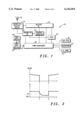
- FIG. 1 illustrates schematically, in block diagram form, components of a cellular telephone apparatus
- FIG. 2 illustrates, in graphical form, voltage levels encountered during a momentary interruption of supplied power level
- FIG. 3 illustrates a state diagram of an electronic apparatus in accordance with the invention.
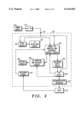
- FIG. 4 illustrates, in block diagram form, a power management circuit in accordance with the invention.
- the invention in its various embodiments, is applicable to a wide variety of electronic apparatus, but for ease of understanding the invention will be explained and illustrated with reference to its application to a particular type of electronic apparatus, namely a portable cellular telephone.
- the invention is not limited to this illustrative embodiment and is intended to include all varieties of electronic apparatus as well as the individual components that make up such apparatus, including, for example, the power management integrated circuit to be described below.
- the present invention provides a system providing for restoration of operation of an electronic apparatus following disconnection and reconnection of a power supply coupled to the electronic apparatus, the system comprising: a terminal coupled to the apparatus for receiving a voltage from the power supply; an internal reference supply circuit coupled to the terminal and capable of providing a voltage reference; a first level detecting circuit coupled to the terminal and capable of operating independently of the internal reference supply circuit for monitoring the voltage; a second level detecting circuit coupled to the terminal for monitoring the voltage; a power cut monitor and reference control circuit coupled to receive a first signal from the first level detecting circuit and a second signal from the second level detecting circuit and capable of causing the internal reference supply circuit to remain enabled in response to the first signal and the second signal indicating the voltage is lower than a first predetermined voltage level and greater than a second predetermined voltage level; and an under voltage monitor and recovery circuit coupled to receive a third signal from the second level detecting circuit and capable of causing the electronic apparatus to restart if the voltage monitored by the second level detecting circuit drops below the first predetermined voltage level
- the present invention provides a method for recovering from an interruption in voltage level of power supplied to an electronic apparatus that is in a predetermined state and that includes an internal reference supply for powering a recovery system and an external reference supply for powering the apparatus, the method comprising: monitoring the voltage level of power supplied to the electronic apparatus; maintaining the internal reference supply in an enabled state if the voltage level is below a first predetermined voltage level and above a second predetermined voltage level; shutting down the external reference supply when the voltage level is below the first predetermined voltage level and above the second predetermined low voltage level; and returning the electronic apparatus to the predetermined state in response to the voltage level increasing to a level greater than the first predetermined voltage level.
- FIG. 1 illustrates schematically the various components of a cellular telephone 20.
- the cellular telephone includes an antenna 22 for the receipt and transmission of cellular telephone signals.
- Antenna 22 is coupled to a transmit/receive switch 24 that is operative to transmit or receive telephone signals.
- Switch 24 is coupled to a receiver radio frequency (RF) component 26 and to a transmitter RF component 28 and serves to selectively couple either the receiver component or transmitter component to antenna 22.
- RF receiver component 26 may include an RF filter, RF amplifier, RF mixer, analog-to-digital (A/D) converter, baseband circuits, and the like.
- the RF transmitter component 28 may include elements such as a D/A converter, filter, modulator, mixer, power amplifier, and the like.
- Both receiver component 26 and transmitter component 28 are coupled to a frequency generation component 30.
- Frequency generation component 30 typically includes a number of phase lock loop (PLL) circuits and voltage controlled oscillators for use by the receiver component and the transmitter component.
- PLL
- a logic component 32 that includes a logic device or decision making device (hereinafter referred to as "decision logic”) such as, for example, a microprocessor or microcontroller and may also include a digital signal processor (DSP), memory, and logic circuitry.
- DSP digital signal processor
- Component 32 controls the operation of the telephone.
- Cellular telephone 20 also includes power supply switches 34 or other mechanism to couple the telephone to an external power supply 46.
- Power supply 46 may comprise, for example, a portable battery, an automobile battery adapter, or an AC power supply.
- Power supply 46 is coupled to a terminal 48 of the power supply switches, and through the switches to a power supply input terminal 44 on a power management integrated circuit (IC) 36.
- Power management IC 36 includes, in addition to other components, internal reference supply circuits that provide the regulated power supplies necessary to operate the power management IC itself.
- the power management IC also includes external reference supply circuits for external load use such as to power the RF circuitry, baseband circuits, and the like.
- Power management IC 36 may also be coupled to other components of the cellular telephone such as an earpiece 38, microphone 40 and electroluminescent panel 42.
- FIG. 2 illustrates the effect of a momentary interruption in the supply of power from power supply 46 to power supply switches 34 and therefore to power management integrated circuit 36. The upper portion of FIG.
- FIG. 2 illustrates the voltage measured at terminal 48, the input to the power supply switches. If power supply 46, such as a portable battery, is temporarily disconnected from terminal 48 at time t 1 , the voltage measured at that terminal abruptly drops to zero. If the momentary interruption ends at time t 2 , the voltage applied to terminal 48 returns to its normal value at that time.
- the lower portion of FIG. 2 illustrates the B+ voltage measured at terminal 44 in response to such a momentary disconnection of power supply 46. As indicated, the B+ voltage begins to decay at time t 1 and is restored to its full value at time t 2 .
- Power management integrated circuit 36 can include a power on reset (POR) circuit.
- the function of the power on reset circuit is to restart the electronic apparatus in a controlled manner after an interruption in power.
- the power on reset circuit functions, however, only in response to the B+ voltage falling below a prescribed value such as that indicated in FIG. 2. If the B+ voltage falls below the POR level, all circuits are shut down and upon reapplication of the power, the POR circuit restarts each of the individual circuits within the electronic apparatus in an orderly manner. The electronic apparatus thus restarts in a manner similar to the initial turning on of the apparatus.
- the POR circuit is not activated and, in the prior art systems, the telephone may not be restored to its desired state.
- the B+ voltage falls to a value below an under voltage (UV) value but above the POR voltage
- functionality of the telephone cannot be guaranteed upon reapplication of the power supply.
- the UV value is the minimum value necessary to guarantee that the circuitry in logic component 32, the voltage controlled oscillators in component 30, and the like in other components, maintain proper functional values.
- Functional restart cannot be guaranteed because the status of the logic circuitry and other components may be indeterminate, in turn, because the voltage supplied to the reference circuits dropped below the minimum value to guarantee functionality, but not below the POR level to invoke a full shut down and restart.
- a system and method are provided for the controlled recovery of an electronic apparatus, such as a cellular telephone, following a momentary interruption in the voltage level supplied by an external power supply.
- the momentary interruption can be caused, for example, by a momentary mechanical disconnect of the battery from the cellular telephone, either intentional or accidental.
- a momentary interruption of power is referred to as a "power cut.”
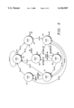
- FIG. 3 illustrates a state diagram in accordance with one embodiment of the invention in conjunction with FIG. 4 that schematically illustrates components of an integrated system in accordance with an embodiment of the invention.
- the components illustrated in FIG. 4 comprise components in an improved power management integrated circuit 36.
- FIG. 3 illustrates a state diagram for an electronic apparatus, here a cellular telephone, including both normal modes of operation and power cut modes.
- the power cut modes include controlled recovery from those power cut modes.
- State 0, indicated by the numeral 60 represents the condition in which the B+ voltage at terminal 44 is below a low voltage (LV) set point.
- the LV set point is set equal to the POR level, although other voltage levels could be selected.
- the B+ voltage at terminal 44 can be below the LV set point, for example, if the battery has been drained by extensive use, if the battery is defective, or if the battery has been removed.
- state 0 the cellular telephone is non-functional.
- the B+ voltage is above the LV set point, but is below the UV set point value.
- the UV set point value is the minimum voltage value necessary to insure that the cellular telephone circuitry maintains functional values.
- the internal and external reference supply circuits of the power management IC are enabled. Below this voltage value, however, the B+ voltage is-insufficient to generate proper external reference supply voltages to power various loads in the cellular telephone unit so the decision logic in logic component 32 is maintained in a reset state.
- State 3 is the "ON" state for the cellular telephone.
- the cellular telephone may be operated in the normal telephone manner. From state 3 the cellular telephone may be turned “OFF” (state 4) or, if the power cut system senses that a power interruption has occurred (i.e., that the B+ voltage is less than the UV set point), the power management integrated circuit 36 is placed in a power cut state (state 5), as discussed below.
- State 4 is the "OFF" state of the cellular telephone.
- the power management integrated circuit is maintained in a low power state unless the battery is either removed and B+ voltage drains to a level such that it is less than the level of the LV set point (i.e., state 0), or an "ON" request is received from the user through the decision logic.
- state 5, indicated by the numeral 70, and state 6, indicated by the numeral 72, to be described below handle a power interruption to the cellular telephone of any duration. As will be explained, this is done without the need for external components or additional significant power consumption and is completely transparent to the user. That is, there are no awkward delays in resumption of cellular telephone operation following the termination of a power supply disruption.
- a power supply 46 provides a source of power to terminal 44 of the power management integrated circuit 36 by way of power supply switches 34.
- An analog level detection circuit 80 detects and monitors the voltage supplied by power supply 46 and operates independently of the state of any of the internal or external references. This operation begins in state 0.
- the output of level detection circuit 80 is coupled to a LV detection logic circuit 82 and to a power cut monitor and reference control circuit 84.
- the output of power cut monitor and reference control circuit 84 is coupled to internal reference supply circuit 86 and to a UV monitor and recovery circuit 88.
- the output of the internal reference supply circuit 86 is coupled to a precision UV detection circuit 90.
- UV detector 90 is dependent on the internal references and, in accordance with the invention, continues to sense the power supply value in anticipation of any power interruption from power supply 46.
- Precision UV detection circuit 90 also has an input coupled to terminal 44 and provides accurate voltage sensing of the B+ voltage at terminal 44. The UV detection circuit 90 is thus dependent on the availability of voltage and current references.
- UV detection circuit 90 operating from the internal reference supplies, is able to provide a more precise measurement of the applied voltage than is level detection circuit 80.
- the output of precision UV detection circuit 90 is coupled to a microprocessor interface 92 and to UV monitor and recovery circuit 88.
- Microprocessor interface 92 is coupled to the decision logic contained in logic circuit 32. In addition to other functions controlled by the decision logic, the decision logic in circuit 32 is also coupled to a watchdog circuit 94.
- the UV monitor and recovery circuit 88 is coupled to a restart circuit 96.
- the power management integrated circuit enters state 5 when the battery voltage is detected by UV detector 90 to have dropped below the UV set point. All internal and external references are maintained enabled in state 5. Maintenance of the internal and external references is driven by a decision made in the power cut monitor and reference control circuit 84 in recognition that a power cut has occurred as indicated by a signal provided by precision UV detection circuit 90. Upon detection of the UV condition by UV detector 90, a request is sent to the decision logic through microprocessor interface 92 to notify the decision logic 32 that a shut down of external references would be prudent.
- the power management integrated circuit would move to state 2 and allow the decision logic to place the cellular telephone in the state that existed prior to the power interruption.
- the threshold for voltage detection necessary to cause the transition to state 2 is usually set at a value substantially equal to the UV level, but slightly higher or lower than the UV level.
- the threshold can be set, for example at about 50-100 millivolts above or below the UV level.
- the transition to state 2 is accomplished by a signal provided by UV monitor and recovery circuit 88 to the restart circuit 96.
- Such a restart is seamless and transparent to the user and corrects for any momentary interruptions such as those caused by repeated mechanical jarring of the cellular telephone and battery.
- a further drop in battery voltage below the LV set point causes the cellular telephone to transition to state 0.
- the cellular telephone enters state 5 from either state 3 or state 2 if the voltage detected at terminal 44 falls below a first predetermined UV level. From state 5 the cellular telephone transitions to state 0 if the voltage falls further to a level less than a second predetermined LV level. In state 0 both the internal and external reference supplies are disabled. If the voltage detected at terminal 44 recovers to a level greater than the first predetermined UV level, the cellular telephone can transition from state 5 to state 2.
- the cellular telephone can also transition from state 5 to state 6, indicated by numeral 72, if, while in state 5, either no response is received from the decision logic within a certain predetermined length of time (a "timeout" condition) to indicate that the decision logic understands that a loss of power has occurred or, the decision logic acknowledges the power loss.
- the cellular telephone returns to state 2 and awaits a command from the decision logic indicating the state in which the cellular telephone should be placed.
- the system is placed in state 0 and waits reapplication of a functional battery. In this case the voltage supplied by the battery has dropped below the allowed minimum voltage of the entire system and a new start up sequence would be required to restart the cellular telephone and to place all of the circuits in the proper operating condition. Transitioning from state 6 to state 0 in this manner would not necessarily be considered a power cut, but could also be the result of a complete and total depletion of the battery pack or the removal of the battery by a user for replacement, repair or other such normal operation.
- transitions are indicated in the state diagram illustrated in FIG. 3. For example, if the cellular telephone is in state 0, the cellular telephone will remain in state 0 if the battery voltage detected at terminal 44 remains less than the predetermined LV level. If the cellular telephone is at state 1, the cellular telephone will return to state 0 if the voltage detected at terminal 44 decreases to a value less than the predetermined LV set point.
- the cellular telephone can transition to either state 3 or state 4 depending on the response received from the decision logic in logic circuit 32.
- the decision logic can send a signal to watchdog circuit 94 indicating that the cellular telephone should turn “ON", state 3 (i.e., watchdog circuit 94 indicates “ON") or that the cellular telephone should turn “OFF” (i.e., watchdog indicates “OFF”). If the watchdog circuit signals "OFF,” at least the external references are disabled.
- the cellular telephone will remain in that state if the voltage detected at terminal 44 remains greater than the predetermined UV set point level and if the watchdog continues to indicate the "ON" state. If the watchdog circuit, instead, indicates the "OFF" state, the cellular telephone will transition from state 3 to state 4.
- the cellular telephone If the cellular telephone is in state 4, it will remain in state 4 if there is no stimulus requesting the telephone to turn “ON.” If there is an "ON" request, such as the user pressing the power key, the cellular telephone will transition from state 4 to state 1.
- LV level detect circuit 80 and precision UV level detect circuit 90 are preferably implemented using conventional analog techniques.
- Power cut monitor and reference control circuit 84, and UV monitor and recovery circuit 88 are preferably implemented using digital logic gates. Accordingly, illustrative circuit diagrams are not deemed necessary.
- the power supply usually provides a voltage of about 3.8 volts.
- the voltage detected at terminal 44, the B+ voltage, is normally about 3.6 volts.
- the predetermined UV level is set to a level of about 2.7 volts and the second predetermined LV level is set to about 2.0 volts, the same as the POR value.
Abstract
Description
Claims (19)
Priority Applications (1)
| Application Number | Priority Date | Filing Date | Title |
|---|---|---|---|
| US09/514,800 US6144569A (en) | 2000-02-29 | 2000-02-29 | System and method for recovering from a power supply interruption |
Applications Claiming Priority (1)
| Application Number | Priority Date | Filing Date | Title |
|---|---|---|---|
| US09/514,800 US6144569A (en) | 2000-02-29 | 2000-02-29 | System and method for recovering from a power supply interruption |
Publications (1)
| Publication Number | Publication Date |
|---|---|
| US6144569A true US6144569A (en) | 2000-11-07 |
Family
ID=24048749
Family Applications (1)
| Application Number | Title | Priority Date | Filing Date |
|---|---|---|---|
| US09/514,800 Expired - Lifetime US6144569A (en) | 2000-02-29 | 2000-02-29 | System and method for recovering from a power supply interruption |
Country Status (1)
| Country | Link |
|---|---|
| US (1) | US6144569A (en) |
Cited By (7)
| Publication number | Priority date | Publication date | Assignee | Title |
|---|---|---|---|---|
| EP1441531A1 (en) * | 2003-01-22 | 2004-07-28 | Pace Micro Technology PLC | Method and apparatus for power supply to a low noise block (LNB) |
| US20060197681A1 (en) * | 2005-03-03 | 2006-09-07 | Denso Corporation | In-vehicle emergency report device |
| US20080068212A1 (en) * | 2006-08-30 | 2008-03-20 | Boon Hou Tay | Coupling point temperature and current measuring system |
| WO2008132558A1 (en) * | 2007-04-26 | 2008-11-06 | Freescale Semiconductor, Inc. | Microcontroller unit and method therefor |
| WO2012099799A1 (en) * | 2011-01-17 | 2012-07-26 | Qualcomm Incorporated | Booting a mobile electronic device with a low battery based on a dynamic boot threshold |
| JP2015018303A (en) * | 2013-07-09 | 2015-01-29 | カシオ計算機株式会社 | Electronic apparatus, control method of electronic apparatus, and program |
| WO2019082787A1 (en) * | 2017-10-26 | 2019-05-02 | 株式会社デンソー | Communication device |
Citations (7)
| Publication number | Priority date | Publication date | Assignee | Title |
|---|---|---|---|---|
| US4982149A (en) * | 1989-01-11 | 1991-01-01 | Kabushiki Kaisha Toshiba | Electric supply apparatus having means for correcting supply voltage fluctuations |
| US5661780A (en) * | 1995-07-12 | 1997-08-26 | Uniden Corporation | Cordless telephone having power failure detection circuit |
| US5696817A (en) * | 1991-12-09 | 1997-12-09 | Canon Kabushiki Kaisha | Apparatus and method for determining the source of a telephone communication |
| US5955843A (en) * | 1997-06-24 | 1999-09-21 | Hubbell Incorporated | Relay circuit for providing power from a normal or emergency power supply to ignite and drive a high intensity discharge lamp |
| US5963015A (en) * | 1997-05-21 | 1999-10-05 | Samsung Electronics Co., Ltd. | External battery charger for use with a battery powered electronic device and an extra battery |
| US5977659A (en) * | 1996-06-03 | 1999-11-02 | Canon Kabushiki Kaisha | Inverter apparatus and solar power generation apparatus |
| US6018802A (en) * | 1993-08-31 | 2000-01-25 | Canon Kabushiki Kaisha | Communication apparatus having power backup function for image memory |
-
2000
- 2000-02-29 US US09/514,800 patent/US6144569A/en not_active Expired - Lifetime
Patent Citations (7)
| Publication number | Priority date | Publication date | Assignee | Title |
|---|---|---|---|---|
| US4982149A (en) * | 1989-01-11 | 1991-01-01 | Kabushiki Kaisha Toshiba | Electric supply apparatus having means for correcting supply voltage fluctuations |
| US5696817A (en) * | 1991-12-09 | 1997-12-09 | Canon Kabushiki Kaisha | Apparatus and method for determining the source of a telephone communication |
| US6018802A (en) * | 1993-08-31 | 2000-01-25 | Canon Kabushiki Kaisha | Communication apparatus having power backup function for image memory |
| US5661780A (en) * | 1995-07-12 | 1997-08-26 | Uniden Corporation | Cordless telephone having power failure detection circuit |
| US5977659A (en) * | 1996-06-03 | 1999-11-02 | Canon Kabushiki Kaisha | Inverter apparatus and solar power generation apparatus |
| US5963015A (en) * | 1997-05-21 | 1999-10-05 | Samsung Electronics Co., Ltd. | External battery charger for use with a battery powered electronic device and an extra battery |
| US5955843A (en) * | 1997-06-24 | 1999-09-21 | Hubbell Incorporated | Relay circuit for providing power from a normal or emergency power supply to ignite and drive a high intensity discharge lamp |
Cited By (12)
| Publication number | Priority date | Publication date | Assignee | Title |
|---|---|---|---|---|
| EP1441531A1 (en) * | 2003-01-22 | 2004-07-28 | Pace Micro Technology PLC | Method and apparatus for power supply to a low noise block (LNB) |
| US20060197681A1 (en) * | 2005-03-03 | 2006-09-07 | Denso Corporation | In-vehicle emergency report device |
| US7751796B2 (en) * | 2005-03-03 | 2010-07-06 | Denso Corporation | In-vehicle emergency report device |
| US20080068212A1 (en) * | 2006-08-30 | 2008-03-20 | Boon Hou Tay | Coupling point temperature and current measuring system |
| US7808774B2 (en) * | 2006-08-30 | 2010-10-05 | Boon Hou Tay | Coupling point temperature and current measuring system |
| WO2008132558A1 (en) * | 2007-04-26 | 2008-11-06 | Freescale Semiconductor, Inc. | Microcontroller unit and method therefor |
| US8242815B2 (en) | 2007-04-26 | 2012-08-14 | Freescale Semiconductor, Inc. | Microcontroller unit and method therefor |
| WO2012099799A1 (en) * | 2011-01-17 | 2012-07-26 | Qualcomm Incorporated | Booting a mobile electronic device with a low battery based on a dynamic boot threshold |
| US9436479B2 (en) | 2011-01-17 | 2016-09-06 | Qualcomm Incorporated | Booting a mobile electronic device with a low battery based on a dynamic boot threshold |
| JP2015018303A (en) * | 2013-07-09 | 2015-01-29 | カシオ計算機株式会社 | Electronic apparatus, control method of electronic apparatus, and program |
| WO2019082787A1 (en) * | 2017-10-26 | 2019-05-02 | 株式会社デンソー | Communication device |
| US11005506B2 (en) * | 2017-10-26 | 2021-05-11 | Denso Corporation | Communication apparatus |
Similar Documents
| Publication | Publication Date | Title |
|---|---|---|
| US7127228B2 (en) | Portable electric device with power failure recovery and operation method thereof | |
| US5604708A (en) | Fail-safe system for preserving a backup battery | |
| US5963015A (en) | External battery charger for use with a battery powered electronic device and an extra battery | |
| EP0882258B1 (en) | Reset circuit for a battery-powered integrated circuit and method of resetting such integrated circuit | |
| US6643527B2 (en) | Power switching unit of a portable telephone capable of monitoring and controlling a battery supply voltage thereof | |
| US8130698B2 (en) | Changing an operation state and recovering a network of a WLAN device | |
| US5867798A (en) | Cordless telephone system having power interruption detection | |
| US10727544B2 (en) | Uninterruptible power supply and battery activation operation method thereof | |
| US6144569A (en) | System and method for recovering from a power supply interruption | |
| KR100498047B1 (en) | Method and Aparatus for reduce extra current consumption of mobile device | |
| US6765369B2 (en) | Apparatus and method for managing power of a battery | |
| US5831415A (en) | Electrical disconnection and automatic re-engagement of battery monitoring circuits | |
| US6603285B2 (en) | Power circuit, power supply method, and electronic device | |
| US7446434B1 (en) | Dual mode power management system | |
| CA2129581C (en) | Reset recovery in a microprocessor controlled device | |
| JP2002300732A (en) | Secondary battery device | |
| JPH1012283A (en) | Battery pack and its control method | |
| KR20000025277A (en) | Power control circuit of portable electronic apparatus | |
| KR100379616B1 (en) | Backup Battery Power Circuit Of Mibile Telephone | |
| KR20020074496A (en) | Method of powering-up battery powered apparatus | |
| KR100587271B1 (en) | Automatic power on method in mobile terminal | |
| JP2003339125A (en) | Backup power supply control circuit | |
| JP3291159B2 (en) | Portable equipment | |
| JP2687772B2 (en) | Selective call receiver | |
| KR100388955B1 (en) | apparatus and method for currency time extension of wireless telephone at electrostatic |
Legal Events
| Date | Code | Title | Description |
|---|---|---|---|
| AS | Assignment |
Owner name: MOTOROLA, INC., ILLINOIS Free format text: ASSIGNMENT OF ASSIGNORS INTEREST;ASSIGNORS:RODRIGUEZ, DAVID;GRIFFITH, RICHARD S.;REEL/FRAME:010924/0007 Effective date: 20000229 |
|
| STCF | Information on status: patent grant |
Free format text: PATENTED CASE |
|
| FPAY | Fee payment |
Year of fee payment: 4 |
|
| AS | Assignment |
Owner name: FREESCALE SEMICONDUCTOR, INC., TEXAS Free format text: ASSIGNMENT OF ASSIGNORS INTEREST;ASSIGNOR:MOTOROLA, INC.;REEL/FRAME:015698/0657 Effective date: 20040404 Owner name: FREESCALE SEMICONDUCTOR, INC.,TEXAS Free format text: ASSIGNMENT OF ASSIGNORS INTEREST;ASSIGNOR:MOTOROLA, INC.;REEL/FRAME:015698/0657 Effective date: 20040404 |
|
| AS | Assignment |
Owner name: CITIBANK, N.A. AS COLLATERAL AGENT, NEW YORK Free format text: SECURITY AGREEMENT;ASSIGNORS:FREESCALE SEMICONDUCTOR, INC.;FREESCALE ACQUISITION CORPORATION;FREESCALE ACQUISITION HOLDINGS CORP.;AND OTHERS;REEL/FRAME:018855/0129 Effective date: 20061201 Owner name: CITIBANK, N.A. AS COLLATERAL AGENT,NEW YORK Free format text: SECURITY AGREEMENT;ASSIGNORS:FREESCALE SEMICONDUCTOR, INC.;FREESCALE ACQUISITION CORPORATION;FREESCALE ACQUISITION HOLDINGS CORP.;AND OTHERS;REEL/FRAME:018855/0129 Effective date: 20061201 |
|
| FPAY | Fee payment |
Year of fee payment: 8 |
|
| AS | Assignment |
Owner name: CITIBANK, N.A., AS COLLATERAL AGENT,NEW YORK Free format text: SECURITY AGREEMENT;ASSIGNOR:FREESCALE SEMICONDUCTOR, INC.;REEL/FRAME:024397/0001 Effective date: 20100413 Owner name: CITIBANK, N.A., AS COLLATERAL AGENT, NEW YORK Free format text: SECURITY AGREEMENT;ASSIGNOR:FREESCALE SEMICONDUCTOR, INC.;REEL/FRAME:024397/0001 Effective date: 20100413 |
|
| FPAY | Fee payment |
Year of fee payment: 12 |
|
| AS | Assignment |
Owner name: CITIBANK, N.A., AS NOTES COLLATERAL AGENT, NEW YOR Free format text: SECURITY AGREEMENT;ASSIGNOR:FREESCALE SEMICONDUCTOR, INC.;REEL/FRAME:030633/0424 Effective date: 20130521 |
|
| AS | Assignment |
Owner name: CITIBANK, N.A., AS NOTES COLLATERAL AGENT, NEW YOR Free format text: SECURITY AGREEMENT;ASSIGNOR:FREESCALE SEMICONDUCTOR, INC.;REEL/FRAME:031591/0266 Effective date: 20131101 |
|
| AS | Assignment |
Owner name: FREESCALE SEMICONDUCTOR, INC., TEXAS Free format text: PATENT RELEASE;ASSIGNOR:CITIBANK, N.A., AS COLLATERAL AGENT;REEL/FRAME:037356/0553 Effective date: 20151207 Owner name: FREESCALE SEMICONDUCTOR, INC., TEXAS Free format text: PATENT RELEASE;ASSIGNOR:CITIBANK, N.A., AS COLLATERAL AGENT;REEL/FRAME:037354/0225 Effective date: 20151207 Owner name: FREESCALE SEMICONDUCTOR, INC., TEXAS Free format text: PATENT RELEASE;ASSIGNOR:CITIBANK, N.A., AS COLLATERAL AGENT;REEL/FRAME:037356/0143 Effective date: 20151207 |
|
| AS | Assignment |
Owner name: MORGAN STANLEY SENIOR FUNDING, INC., MARYLAND Free format text: ASSIGNMENT AND ASSUMPTION OF SECURITY INTEREST IN PATENTS;ASSIGNOR:CITIBANK, N.A.;REEL/FRAME:037486/0517 Effective date: 20151207 |
|
| AS | Assignment |
Owner name: MORGAN STANLEY SENIOR FUNDING, INC., MARYLAND Free format text: ASSIGNMENT AND ASSUMPTION OF SECURITY INTEREST IN PATENTS;ASSIGNOR:CITIBANK, N.A.;REEL/FRAME:037518/0292 Effective date: 20151207 |
|
| AS | Assignment |
Owner name: MORGAN STANLEY SENIOR FUNDING, INC., MARYLAND Free format text: SUPPLEMENT TO THE SECURITY AGREEMENT;ASSIGNOR:FREESCALE SEMICONDUCTOR, INC.;REEL/FRAME:039138/0001 Effective date: 20160525 |
|
| AS | Assignment |
Owner name: NXP, B.V., F/K/A FREESCALE SEMICONDUCTOR, INC., NETHERLANDS Free format text: RELEASE BY SECURED PARTY;ASSIGNOR:MORGAN STANLEY SENIOR FUNDING, INC.;REEL/FRAME:040925/0001 Effective date: 20160912 Owner name: NXP, B.V., F/K/A FREESCALE SEMICONDUCTOR, INC., NE Free format text: RELEASE BY SECURED PARTY;ASSIGNOR:MORGAN STANLEY SENIOR FUNDING, INC.;REEL/FRAME:040925/0001 Effective date: 20160912 |
|
| AS | Assignment |
Owner name: NXP B.V., NETHERLANDS Free format text: RELEASE BY SECURED PARTY;ASSIGNOR:MORGAN STANLEY SENIOR FUNDING, INC.;REEL/FRAME:040928/0001 Effective date: 20160622 |
|
| AS | Assignment |
Owner name: NXP USA, INC., TEXAS Free format text: CHANGE OF NAME;ASSIGNOR:FREESCALE SEMICONDUCTOR, INC.;REEL/FRAME:040652/0241 Effective date: 20161107 Owner name: NXP USA, INC., TEXAS Free format text: MERGER;ASSIGNOR:FREESCALE SEMICONDUCTOR, INC.;REEL/FRAME:040652/0241 Effective date: 20161107 |
|
| AS | Assignment |
Owner name: NXP USA, INC., TEXAS Free format text: CORRECTIVE ASSIGNMENT TO CORRECT THE NATURE OF CONVEYANCE PREVIOUSLY RECORDED AT REEL: 040652 FRAME: 0241. ASSIGNOR(S) HEREBY CONFIRMS THE MERGER AND CHANGE OF NAME;ASSIGNOR:FREESCALE SEMICONDUCTOR, INC.;REEL/FRAME:041260/0850 Effective date: 20161107 |
|
| AS | Assignment |
Owner name: MORGAN STANLEY SENIOR FUNDING, INC., MARYLAND Free format text: CORRECTIVE ASSIGNMENT TO CORRECT THE REMOVE PATENTS 8108266 AND 8062324 AND REPLACE THEM WITH 6108266 AND 8060324 PREVIOUSLY RECORDED ON REEL 037518 FRAME 0292. ASSIGNOR(S) HEREBY CONFIRMS THE ASSIGNMENT AND ASSUMPTION OF SECURITY INTEREST IN PATENTS;ASSIGNOR:CITIBANK, N.A.;REEL/FRAME:041703/0536 Effective date: 20151207 |
|
| AS | Assignment |
Owner name: SHENZHEN XINGUODU TECHNOLOGY CO., LTD., CHINA Free format text: CORRECTIVE ASSIGNMENT TO CORRECT THE TO CORRECT THE APPLICATION NO. FROM 13,883,290 TO 13,833,290 PREVIOUSLY RECORDED ON REEL 041703 FRAME 0536. ASSIGNOR(S) HEREBY CONFIRMS THE THE ASSIGNMENT AND ASSUMPTION OF SECURITYINTEREST IN PATENTS.;ASSIGNOR:MORGAN STANLEY SENIOR FUNDING, INC.;REEL/FRAME:048734/0001 Effective date: 20190217 |
|
| AS | Assignment |
Owner name: NXP B.V., NETHERLANDS Free format text: RELEASE BY SECURED PARTY;ASSIGNOR:MORGAN STANLEY SENIOR FUNDING, INC.;REEL/FRAME:050744/0097 Effective date: 20190903 |
|
| AS | Assignment |
Owner name: MORGAN STANLEY SENIOR FUNDING, INC., MARYLAND Free format text: CORRECTIVE ASSIGNMENT TO CORRECT THE REMOVE APPLICATION11759915 AND REPLACE IT WITH APPLICATION 11759935 PREVIOUSLY RECORDED ON REEL 037486 FRAME 0517. ASSIGNOR(S) HEREBY CONFIRMS THE ASSIGNMENT AND ASSUMPTION OF SECURITYINTEREST IN PATENTS;ASSIGNOR:CITIBANK, N.A.;REEL/FRAME:053547/0421 Effective date: 20151207 |
|
| AS | Assignment |
Owner name: NXP B.V., NETHERLANDS Free format text: CORRECTIVE ASSIGNMENT TO CORRECT THE REMOVEAPPLICATION 11759915 AND REPLACE IT WITH APPLICATION11759935 PREVIOUSLY RECORDED ON REEL 040928 FRAME 0001. ASSIGNOR(S) HEREBY CONFIRMS THE RELEASE OF SECURITYINTEREST;ASSIGNOR:MORGAN STANLEY SENIOR FUNDING, INC.;REEL/FRAME:052915/0001 Effective date: 20160622 |
|
| AS | Assignment |
Owner name: NXP, B.V. F/K/A FREESCALE SEMICONDUCTOR, INC., NETHERLANDS Free format text: CORRECTIVE ASSIGNMENT TO CORRECT THE REMOVEAPPLICATION 11759915 AND REPLACE IT WITH APPLICATION11759935 PREVIOUSLY RECORDED ON REEL 040925 FRAME 0001. ASSIGNOR(S) HEREBY CONFIRMS THE RELEASE OF SECURITYINTEREST;ASSIGNOR:MORGAN STANLEY SENIOR FUNDING, INC.;REEL/FRAME:052917/0001 Effective date: 20160912 |