US6139998A - Transparent substrate for an electrophotographic photoreceptor and an electrophotographic photoreceptor using the same - Google Patents
Transparent substrate for an electrophotographic photoreceptor and an electrophotographic photoreceptor using the same Download PDFInfo
- Publication number
- US6139998A US6139998A US09/271,663 US27166399A US6139998A US 6139998 A US6139998 A US 6139998A US 27166399 A US27166399 A US 27166399A US 6139998 A US6139998 A US 6139998A
- Authority
- US
- United States
- Prior art keywords
- substrate
- transparent substrate
- photoreceptor
- electrophotographic photoreceptor
- cylindrical
- Prior art date
- Legal status (The legal status is an assumption and is not a legal conclusion. Google has not performed a legal analysis and makes no representation as to the accuracy of the status listed.)
- Expired - Lifetime
Links
Images


Classifications
-
- G—PHYSICS
- G03—PHOTOGRAPHY; CINEMATOGRAPHY; ANALOGOUS TECHNIQUES USING WAVES OTHER THAN OPTICAL WAVES; ELECTROGRAPHY; HOLOGRAPHY
- G03G—ELECTROGRAPHY; ELECTROPHOTOGRAPHY; MAGNETOGRAPHY
- G03G5/00—Recording members for original recording by exposure, e.g. to light, to heat, to electrons; Manufacture thereof; Selection of materials therefor
- G03G5/10—Bases for charge-receiving or other layers
Definitions
- the present invention relates to a transparent substrate for an electrophotographic photoreceptor, which is employed in monochromatic and color copiers, monochromatic and color printers, and the like, and an electrophotographic photoreceptor using the same.
- the surface of an electrostatic image forming body which is in the form of a rotating drum or belt, is charged; is exposed imagewise, and is developed to form a toner image on the electrostatic image forming body, which is transferred subsequently to a transfer material, and then fixed.
- the electrostatic image forming body should move at a constant speed under predetermined timing so that the distance and contact pressure situation between the image forming body and each of the charging device, the exposure device, the development device, the transfer device, the charge eliminating device, the cleaning device, etc., which are arranged around the image forming body, are not changed.
- each device should return to the initial position so as to be ready for the subsequent cycle.
- a photoreceptor drum is employed, which is prepared by providing a photosensitive layer on the circumferential surface of an almost cylindrical substrate.
- metals such as aluminum, etc. are employed in most cases.
- the limit has been reached when the cylindrical substrate is produced by machining, employing metals.
- plastics are light in weight and low in cost, as the material of the photoreceptor substrate, these are considered to be preferred materials.
- a type of apparatus in which exposure is carried out from the inner side of a photoreceptor through a transparent cylindrical substrate is excellent because this type of apparatus is considered to be appropriate for obtaining high quality color image at a high speed and a compact image forming apparatus.
- Japanese Patent Publication Open to Public Inspection No. 8-202067 proposes a method which produces a transparent and accurate substrate employing a synthetic resin being light in weight with excellent shock resistance, and low in cost.
- plastics which are employed to produce a photoreceptor substrate, preferably have thermal resistance, including flame resistance or incombustibility.
- An object of the present invention is to provide a transparent substrate for an electrophotographic photoreceptor, which, when an image is exposed through its photoreceptor substrate, minimizes image blur and image distortion, and exhibits good adhesion of the electrically conductive layer with the substrate, excellent resolving power, and durability of the finished image, and to provide a production method thereof, and an electrophotographic photoreceptor, an image forming method, and an image forming apparatus using the same.
- Another object of the present invention is to provide a transparent substrate for an electrophotographic photoreceptor, which exhibits high transparency without optical distortion, high humidity and heat resistance, minimum deformation of the substrate, excellent dimensional stability, and results in no deterioration of electrophotographic performance and image quality when repeatedly employed, and a production method thereof, and to provide an electrophotographic photoreceptor, an image forming method, and an image forming apparatus using the same.
- Still another object of the present invention is to provide a transparent substrate for an electrophotographic photoreceptor, which exhibits high transparency without optical distortion, minimum deformation of the substrate, excellent dimensional stability, and results in no deterioration of electrophotographic performances when repeatedly employed, and in addition, exhibits high incombustibility, and a production method thereof, and to provide an electrophotographic photoreceptor, an image forming method, and an image forming apparatus using the same.
- the transparent substrate for the electrophotographic photoreceptor of the present invention is cylindrical and made of a polymer resin, and the Rz of the inner surface is not more than 0.5 ⁇ m.
- the Rz of the outer surface of the cylindrical transparent substrate is preferably between 0.2 and 2.0 ⁇ m.
- Polymer resins are preferably vinyl series polymer resins.
- the waviness of the inner surface of the cylindrical transparent substrate is preferably between 0.1 and 5.0 ⁇ m.
- the transparent substrate is preferably formed employing a polymer resin obtained by copolymerizing radical polymerizable monomers using a multifunctional vinyl compound as a cross-linking agent.
- the above-mentioned radical polymerizable monomer is preferably methyl methacrylate.
- the transparent substrate for an electrophotographic photoreceptor
- the transparent substrate is formed employing a cross-linked polymer resin and the double refraction of the aforesaid transparent substrate is not more than 150 nm and the difference in the substrate is preferably within 50 nm.
- the transparent substrate is preferably formed of a polymer resin containing a fire-retardant.
- the transparent substrate is preferably formed of a polymer resin obtained by a centrifugal polymerization method.
- An electrophotographic photoreceptor may be obtained by providing an electrically conductive layer and a photosensitive layer onto the transparent substrate.
- the present electrophotographic photoreceptor may be suitably employed for the use of exposure from inside of the cylindrical substrate in which an exposure light source is provided in the inside of the cylinder forming the transparent substrate, and from this light source.
- the photosensitive layer is provided on the outer surface of the cylinder which is subjected to image exposure through the substrate.
- the surface of the electrophotographic photoreceptor is uniformly charged, and is exposed imagewise and development is repeatedly carried out with each toner having different color to form superimposed multicolor images which are simultaneously transferred, separated, fixed, and the photoreceptor is cleaned.
- the substrate is exposed imagewise from the inside of the cylinder of the transparent substrate and may be employed as an image forming apparatus for forming images.
- FIG. 1 is a diagram describing Rz.
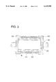
- FIG. 2 is a flow diagram of a production method of the transparent substrate for an electrophotographic photoreceptor of the present invention.
- FIG. 3 is a sectional view showing one example of a production apparatus.
- FIG. 4 is a sectional view of the image forming apparatus of the present invention.
- Japanese Patent Publication Open to Public Inspection No. 8-202067 (employing a centrifugal polymerization method) proposes a production method in which a substrate, which is transparent, dimensionally stable, light in weight, and excellent in shock resistance, is produced employing low cost synthetic resins.
- resin methacrylic acid ester resin and the like are employed, and production and machining are easily carried out and the cost is low. It may certainly be considered as an epoch-making departure, compared with the conventional method.
- the inventors of the present invention have checked the patent and have found that when a photosensitive layer is coated during production of the photoreceptor, the unacceptable surface roughness of the substrate which occurs occasionally causes image blur, uneven density, etc. and it is difficult to obtain clear and sharp images.
- the Rz of the inner surface is preferably between 0.01 and 0.5 ⁇ m.
- the Rz of the outer surface of a transparent substrate is preferably between 0.2 and 2.0 ⁇ m in order to obtain preferred adhesive properties of the layer, e.g. electrically conductive layer, provided on the transparent substrate, to minimize the deterioration of discharge properties of charges during image formation on many sheets, the degrade of image quality and layer peeling, and to obtain sufficient focusing properties and high resolving power and to minimize image blur.
- the layer e.g. electrically conductive layer
- rotation frequency at centrifugal polymerization may be increased, and adjustments may be carried out during the production process, such as the viscosity of the resin solution, polymerization time, etc. or post-processing such as polishing.
- the presence of undulation on the inner surface of the transparent substrate shows that there are internal stress and non-uniform portions. Due to that, when undulation component becomes not less than 0.5 ⁇ m, it should be avoided because keeping quality of the photoreceptor over an extended period of time and mechanical stability of the photoreceptor may be deteriorated. However, in terms of cost, it is not advantageous to decrease the undulation to not more than 0.1 ⁇ m.
- the degree of the undulation is represented by W CM in standard length 0.25 mm of JIS.
- FIG. 3 illustrates one example of the production apparatus.
- C1 is a cylindrical mold and the inner surface is polished to form a cylindrical surface of high accuracy.
- C2 is a heating member and heats the mold C1 from the outside.
- C3 is a mold securing member and clamps the mold C1 from both the right and left and under the clamped state, liquid in the inside of the mold C1 is arranged so as to be not leaked.
- C4 is an injection inlet to which polymerizable liquid materials are poured.
- C5 is a thermometer which measures the inside temperature of C1. This apparatus is structured so that the axis of the mold C1 operates in a horizontal plane and after the polymerizable liquid material is poured, is rotated high speed. Further, after molding the mold, a cylindrical substrate is taken out by moving one side mold securing as shown by arrow B.
- vinyl polymerizable liquid materials in which, for example, methacrylic acid methyl ester monomers are employed as radical polymerizable monomers, and divinylbenzene as a multifunctional vinyl compound and azoisobutylonitrile as a polymerization initiator are added, are subjected to preliminary polymerization under a viscosity between 10 and 400 cp, and are poured into a cylindrical mold C1, which generally has an inner diameter between 20 and 200 mm and a length between 200 and 2,000 mm. Uniform polymerization is enhanced by proper heating while rotating the entire mold.
- the resulting product is annealed and is cooled to near room temperature, and the formed substrate is taken out from the mold, and is cut and is subjected to a surface treatment process, if desired, to complete the production of the transparent substrate for an electrophotographic photoreceptor.
- the above-mentioned centrifugal polymerization method preferably employed in the present invention leaves no die scar on the surface of the cylindrical substrate, and particularly, the inner surface is formed as a natural surface obtained by a centrifugal force, and an extremely smooth inner surface like a glass surface is formed.
- the substrate of the present invention may be obtained by polymerizing or copolymerizing radical polymerizable monomers (monomers which are monomers having no cross-linking properties) or a multifunctional vinyl compound (a monomer having cross-linking properties) in the presence of a radical polymerization initiator.
- radical polymerizable monomers monomers which are monomers having no cross-linking properties
- a multifunctional vinyl compound a monomer having cross-linking properties
- cross-linking is preferably carried out.
- the preferred materials to produce the substrate of the present invention may be obtained by copolymerizing radical polymerizable monomers with multifunctional vinyl compounds (cross-linking monomers) in the presence of a radical polymerization initiator.
- radical polymerizable monomers used in the present invention are side chain alkyl-substituted styrenes such as styrene, a-methylstyrene, m-methylstyrene, p-methylstyrene, etc.; nucleus alkyl-substituted styrenes such as vinyltoluene, etc.; halogenated styrenes such as p-chlorostyrene, o-chlorostyrene, m-chlorostyrene, p-bromostyrene, o-bromostyrene, m-bromostyrene, 2,4-dichlorostyrene, 2,4-bromostyrene, 4-chloro- ⁇ -methylstyrene, 4-bromo- ⁇ -methylstyrene, 2,4,6-trichlorostyrene, 2,4,6-tribromostyrene, pentachlorostyrene
- polyester resins In order to increase Rockwell hardness to not less than 80, listed as those most preferred are polyester resins, polyphenylene sulfide resins, polycarbonate resins, polysulfone resins, methacrylic series resins, acrylic series resins, styrene series resins, etc.
- multifunctional vinyl compounds (monomers having cross-linking properties), at least one selected from those described below is employed as a cross-linking agent; divinylbenzene, methadivinylbenzene, 4,4'-divinylbiphenyl, 3,3'-divinylbiphenyl, 3,4'-divinylbiphenyl, ethylene glycol methacrylate, ethylene glycol acrylate, diethylene glycol methacrylate, diethylene glycol acrylate, 1,4-butanediol methacrylate, 1,4-butanediol acrylate, trimethylolpropane trimethacrylate, trimethylolpropane triacrylate, pentaerythritol tetramethacrylate, pentaerythritol tetracrylate, divinyl phthalate, diallyl phthalate, divinyl isophthalate, diallyl isophthalate, divinyl terephthalate, dial
- the employed addition amount of the cross-linking agents is in the range of 0.05 to 90 weight percent of all monomers (radical polymerizable monomers+ multifunctional vinyl compounds) in raw materials. When the addition amount is less than 0.05 weight percent, heat resistance is not satisfied. When the addition amount is not less than 90 weight percent, mechanical durability is degraded due to the formation of a hard but brittle polymer resin.
- radical polymerization initiators which are employed during polymerization of the polymer resin for the substrate employed in the present invention and those are acceptable, which generate active radicals when applied by active energy rays such as visible light, infrared ray, ultraviolet ray, microwave, electron ray, etc. or heat.
- Radical polymerization initiators which generate active radicals in the presence of heat, include benzoyl peroxide, diisopropylperoxydicarbonate, t-butylperoxy-2-ethyl hexanoate, t-butylperoxypivalate, t-butylperoxydiisobutylate, lauroyl peroxide, t-butylperoxyacetate, t-butylperoxyoctoate, t-butylperoxybenzoate, di-t-butyl peroxide, azobisisobutylonitrile, etc.
- Radical polymerization initiators which generate active radicals in the presence of the active energy rays, include acetophenone, benzophenone, benzoin, benzoin methyl ether, 2-hydroxy-2-methyl-1-phenylpropane-1-on, hydroxycyclohexyl phenyl ketone, methylphenylglyoxylate, 2,4,6-trimethylbenzoyldiphenyl, which can be employed individually or in combination.
- the mixing ratio of the above-mentioned radical polymerization initiators varies depending on the types of radical polymerization initiators, the types of vinyl series monomers, the polymerization hardening temperature, etc. Generally, however, 0.01 to 8 parts by weight to 100 parts by weight of copolymerizable vinyl series monomer is preferred, and 0.1 to 5 parts by weight are particularly preferred.
- the mixing ratio of the above-mentioned radical polymerization initiators of less than 0.01 part by weight is not preferred because polymerization hardening takes a long time or the polymerization is at times not even completed.
- the mixing ratio of the polymerization initiators of not less than 8 parts by weight is not preferred because the resulting polymer becomes brittle or is colored.
- polymers other than the vinyl series polymers include polyamides, polyimidos, epoxy resins, polycarbonates, polysulfones, polyethersulfones, polyesters, polyarylates, polyphenylene oxides, polybutylene terephthalates, polyethylene terephthalates, polymetylpentens, etc.
- the transparent cylindrical substrate of the present invention may be produced by obtaining the desired Rz through polishing or machining the surface.
- vinyl series polymers which are not cross-linked may be used as substrate materials employing the above-mentioned molding method.
- the substrate itself is preferred to be optically uniform. Low double refraction and minimum difference among portions of the substrate are preferred. In practice, no problem is caused regarding optical uniformity and no anisortopic portions are produced.
- the substrate is preferred which has a double refraction of not more than 150 nm or has a difference due to portions of not more than 50 nm. More preferably, the double refraction is to be not more than 100 nm, and the dispersion is to be 20 nm, and most preferably, the double refraction is to be not more than 30 nm, and the dispersion is to be not more than 10 nm.
- the double refraction is adjusted through the selection of monomers, further, polymerization conditions, e.g. temperature during polymerization, stirring conditions, time management, and adjustment of residual stress decrease due to molecular orientation in the annealing process.
- polymerization conditions e.g. temperature during polymerization, stirring conditions, time management, and adjustment of residual stress decrease due to molecular orientation in the annealing process.
- the double refraction can be measured by employing well known methods with the use of an Abbe's refractometer, a strain meter (for example, Accurate Distortion Meter SVP-30 manufactured by Toshiba Corp.), an ellipsometer, etc. Measurement may be carried out so that the maximum and minimum values are found from all positions of the photoreceptor substrate. In practice, measurements are carried out for positions at the central part of the substrate and at both ends, which are involved in image formation.
- a substrate When incombustible materials are used, a substrate can be obtained by copolymerizing a radical polymerizable monomer, a multifunctional vinyl compound, and a fire-retardant in the presence of a radical polymerization initiator.
- fire-retardants employed in the present invention, are various types of compounds containing elements such as P, halogens, N, S, Sb, B, etc. These may be employed individually or in combinations of at least two of those listed.
- inorganic series fire-retardants include compounds containing antimony such as antimony trioxide, antimony tetraoxide, antimony pentaoxide, antimonic acid soda, etc., alumina hydrate, magnesium hydroxide, zinc borate, barium borate, etc.
- antimony trioxide such as antimony trioxide, antimony tetraoxide, antimony pentaoxide, antimonic acid soda, etc.
- alumina hydrate such as magnesium hydroxide, zinc borate, barium borate, etc.
- organic series fire-retardants are more preferred in terms of incombustible effects.
- halogen series fire-retardants include, for example, chlorinated paraffin, chlorinated polyolefin, chlorinated polyethylene, chlorinated polyphenyl, chlorinated oil, perchlorocyclopentadecane, hexabromobenzene, decabromodiphenyl oxide, octabromodiphenyl oxide, pentabromodiphenyl oxide, polydibromophenylene oxide, bis(tribromophenoxy)ethane, ethylenebis-dibromonorubornanedicarboxyimide, dibromoneopentyl glycol tetracarbonate, brominated bisphenol series carbonate oligomer, brominated bisphenol series epoxy resin, brominated bisphenol series phenoxy resin, brominated polystyrene, tetrachlorophthalic anhydride, tetrabromophthalic anhydride, ethylenebis-tetrabromophthalimide, bis(
- phosphorus series fire-retardants there are triarylphosphoric acid esters, diarylphosphoric acid esters, monoarylphosphoric acid esters, arylphosphonic acid compounds, arylphosphone oxide compounds, condensed arylphosphoric acid esters, etc.
- fire-retardants containing a phosphorous atom include butyl pyrophosphate, butyl acid phosphate, butoxyethyl acid phosphate, 2-ethylhexyl acid phosphate, guanylurea phosphate, guanidine phosphate, trimethyl phosphate, tributyl phosphate, trioctyl phosphate, tributoxyethyl phosphate, triphenyl phosphate, diphenyloctyl phosphate, triallyl phosphate, tricresyl phosphate, cresyldi-2,6-xylenyl phosphate, diphenylcresyl phosphate, diethylbis(hydroxyethyl)aminomethyl phosphate, tris(3-hydroxypropyl)phosphine oxide, dibutylhydroxymethyl phosphonate, di(butoxy)phosphinyl-propylamide, dimetylmethyl
- di-(polyoxyethylene)-hydroxymethyl-phosphonate 9,10-dihydro-9-oxtha-10-phosphaphenanthrene-10-oxide
- phenyl phosphonic acid phosphorous-containing polyols
- aromatic polyphosphates melamine phosphoric acid salts
- polyphosphoric acid ammonium etc.
- phosphorous containing series fire-retardants contain no halogen, they are preferred as materials friendly to the circumstance.
- Halogen containing phosphoric acid ester series fire-retardants contain halogen atoms such as chlorine or bromine in the structural unit of phosphate, polyphosphate, polyphosphonate, which include halogenated alkyl phosphoric acid esters, halogen-containing condensed phosphoric acid esters, for example, CR-380, CR-387, CR-530 (these manufactured by Daihachi Kagaku Kogyo Co.), etc. There are halogen containing condensed phosphonic acid esters, halogen containing phosphorous acid esters, etc.
- chlorophosphate bromophosphate, trischloroethyl phosphate, dibromopropyl phosphate, trischloropropyl phosphate, tri(2,3-dibromopropyl)phosphate, bis(2,3-dibromopropyl)2,3-dichloropropyl phosphate, bis(chloropropyl)octyl phosphate, tris( ⁇ -chloroethyl)phosphate, tris(dichloropropyl)phosphate, tris(tribromoneopentyl)phosphate, tris(2,4,6-tribromophenyl)phosphate, bischloroethyl dichloropropyl phosphate, halogenated alkylpolyphosphate, halogenated alkylpolyphosphate, etc.
- R 1 and R 2 each represents a monovalent hydrocarbon group which may contain a halogen atom, a phosphorous atom, or an oxygen atom, or a hydrogen atom, or represents a divalent hydrocarbon group formed by the combination of both, which may contain a halogen atom, a phosphorous atom, or an oxygen atom.
- R 1 and R 2 each represents a monovalent hydrocarbon group which may contain a halogen atom, a phosphorous atom, or an oxygen atom, or a hydrogen atom, or represents a divalent hydrocarbon group formed by the combination of both, which may contain a halogen atom, a phosphorous atom, or an oxygen atom.
- the monovalent hydrocarbon group which may contain a halogen atom, a phosphorous atom, or an oxygen atom, or a hydrogen atom are preferably a halogenoalkyl group having from 1 to 20 carbon atoms such as chloromethyl, chloroethyl, chloropropyl, tribromoneopentyl, etc.; a halogenoaryl group having from 6 to 20 carbon atoms such as dibromophenyl, 2,4,6-tribromophenyl, dichlorophenyl, 2,4,6-trichlorophenyl, etc.; a halogenoaralkyl group having from 7 to 20 carbon atoms; a [bis(halogenoalkoxy)phosphinyl] alkyl group having from 3 to 20 carbon atoms such as 1-[bis(2-chloroethoxy)phosphinyl]-1-methylethyl; an alkyl group having from 1 to 20 carbon atoms such as methyl, e
- divalent hydrocarbon groups formed by the combination of R 1 and R 2 which may contain a halogen atom, a phosphorous atom, or an oxygen atom are preferably represented by general formula (2): ##STR2## Wherein R 5 and R 6 each represents a monovalent hydrocarbon group which may contain a halogen atom, or a hydrogen atom.
- the monovalent hydrocarbon groups represented by R 5 and R 6 which may contain a halogen atom are preferably a halogenoalkyl, halogenoaralkyl, alkyl, aryl or aralkyl group having from 1 to 20 carbon atoms previously exemplified in R 1 and R 2 .
- Phosphoric acid esters which are represented by general formulas (2) through (6) described below are preferred.
- R 7 represents a monovalent hydrocarbon group which may contain a halogen atom or a hydrogen atom
- R 8 and R 9 each represents a monovalent hydrocarbon group which may contain a halogen atom or a hydrogen atom, or represents a divalent hydrocarbon group formed by the combination of both, which may contain a halogen atom.
- at least one of R 7 , R 8 , and R 9 is a divalent hydrocarbon group having a halogen atom, which is formed individually or in combination.
- R 10 and R 11 each represents a monovalent hydrocarbon group which may contain a halogen atom or a hydrogen atom, or represents a divalent hydrocarbon group formed by the combination of both, which may contain a halogen atom
- R 12 represents a monovalent hydrocarbon group which may contain a halogen atom or a hydrogen atom
- R 13 and R 14 each represents a monovalent hydrocarbon group which may contain a halogen atom or a hydrogen atom, or represents a divalent hydrocarbon group formed by the combination of both, which may have a halogen atom.
- At least one of R 10 , R 11 , R 12 , and R 14 is a monovalent or divalent hydrocarbon group having a halogen atom, which is formed individually or in combination and "m" represents an integer of 0 to 5.
- R 15 and R 16 each represents a monovalent hydrocarbon group which may contain a halogen atom or a hydrogen atom, or represents a divalent hydrocarbon group formed by the combination of both, which may contain a halogen atom
- R 17 and R 19 each represents a divalent hydrocarbon group which may have a halogen atom
- R 18 represents a monovalent hydrocarbon group which may contain a halogen atom or a hydrogen atom
- R 20 and R 21 each represents a monovalent hydrocarbon group which may contain a halogen atom or a hydrogen atom, or represents a divalent hydrocarbon group formed by the combination of both, which may have a halogen atom.
- "n" represents an integer of 0 to 5.
- R 25 and R 26 each represents a monovalent hydrocarbon group which may contain a halogen atom or a hydrogen atom, or represents a divalent hydrocarbon group formed by the combination of both, which may contain a halogen atom
- R 27 and R 29 each represents a divalent hydrocarbon group which may have a halogen atom or a hydrogen atom
- R 28 represents a monovalent hydrocarbon group which may contain a halogen atom or a hydrogen atom
- R 30 and R 31 each represents a monovalent hydrocarbon group which may contain a halogen atom or a hydrogen atom, or represents a divalent hydrocarbon group formed by the combination of both, which may have a halogen atom.
- the monovalent hydrocarbon groups which may have a alogen atom which are represented by each of the above-mentioned R 7 , R 8 , R 9 , R 10 , R 11 , R 12 , R 13 , R 14 , R 15 , R 16 , R 18 , R 20 , R 21 , R 22 , R 23 , R 25 , R 26 , R 28 , R 30 , and R 31 , are preferably a halogenoalkyl, halogenoaryl, halogenoaralkyl, alkyl, aryl, or aralkyl group having from 1 to 20 carbon atoms, exemplified above regarding R 1 and R 2 .
- Divalent hydrocarbon groups which may have a halogen atom, which is formed by the combination of the above-mentioned R 8 and R 9 , R 10 and R 11 , R 13 and R 41 , R 15 and R 16 , R 20 and R 21 , R 25 and R 26 , and R 30 and R 31 are preferably those groups exemplified above regarding R 1 and R 2 .
- Divalent hydrocarbon groups which may have a halogen atom which are represented by each of R 17 , R 19 , R 27 , and R 29 are preferably divalent saturated aliphatic hydrocarbon groups having from 1 to 20 carbon atoms such as methylene, ethylidene, isopropylidene, etc.; divalent aromatic hydrocarbon group having from 6 to 20 carbon atoms such as phenylene, methylphenylene, etc.; divalent saturated aliphatic hydrocarbon groups containing a halogen atom having from 2 to 20 carbon atoms; divalent aromatic hydrocarbon groups containing a halogen atom having from 6 to 20 carbon atoms; etc.
- x-valent hydrocarbon groups which may have a halogen atom which is represented by the above-mentioned R 24 are preferably divalent saturated aliphatic hydrocarbon groups which may have a halogen atom such as ethylene, trimethylene, 2,2-dimethyltriethylene, 2,2-bis(chloromethyl)trimethylene, 2,2-bis(bromomethyl)trimethylene, etc.; trivalent saturated aliphatic hydrocarbon groups having from 3 to 20 carbon atoms which may have a halogen atom such as groups represented by CH 3 --C(--CH 2 --) 3 , CH 3 CH 2 --C(--CH 2 --) 3 ; etc.
- the employed amount of these fire-retardants is between 1 and 50 parts by weight to 100 parts by weight entire resins; is more preferably between 3 and 45 parts by weight, and more preferably between 7 and 40 parts by weight.
- the amount exceeds 50 parts by weight, the strength, heat-resistant temperature, keeping quality, repeated use stability, and mechanical physical properties may occasionally be deteriorated.
- the amount is not more than one part by weight, the incombustible effect may occasionally be lowered.
- the practical added amount is appropriately determined in accordance with the desired level regarding incombustibility, mechanical and heat resistance physical properties, and transparency. For example, it is preferred to select them so as to be in V-0 Class of UL-94 Standard.
- the fire-retardant-containing photoreceptor substrate of the present invention is naturally provided with incombustibility.
- the transparent substrate of the present invention is employed for an electrophotographic photoreceptor.
- the surface of the cylindrical substrate of the present invention is smooth. Particularly, when methacrylic acid methyl ester polymer is employed, the transparency is markedly excellent and the strength is high. Accordingly, the resulting substrate is suitable for the image forming apparatus employing a mechanism in which exposure is carried out from the inside.
- the representative photoreceptor is one in which an electrically conductive layer and a photoconductive photosensitive layer are provided onto the surface of a cylindrical substrate, and conventional methods can widely be employed to provide the electrically conductive layer and the photoconductive photosensitive layer.
- electrically conductive transparent layer forming method vacuum evaporation or spattering of metal or metallic oxides such as aluminum, ITO (indium tin oxide), etc. and coating layer formation of electrically conductive resin obtained by mixing fine ITO or fine electrically conductive alumina particles with a resin are representative.
- an interlayer (a subbing layer) may be provided under a charge generating layer.
- subbing layer materials are alcohol-soluble polyamides, copolymerized nylon, alkoxymethylated nylon, vinyl chloride-vinyl acetate copolymers, casein, polyvinyl alcohol, cellulose, gelatin, or as described in Japanese Patent Publication Open to Public Inspection No. 9-68870, a hardening type subbing layer employing metal alkoxides, organic metal chelates, silane coupling agents is used. These are coated so that the layer thickness becomes between about 0.01 and about 5 ⁇ m.
- an inorganic photoconductive material layer may be formed employing vacuum evaporation, etc.
- an organic photoconductive material layer is formed by coating an organic photosensitive material which is of a function separation type comprising an organic photoconductive material layer, particularly, comprising a charge transfer material and a charge generating material, particularly, of a type in which each is independently multicoated.
- the charge generating layer (CGL) is formed by dispersing a charge generating material (CGM) into a binder resin as desired.
- CGM charge generating material
- Listed as CGM are metal or metal-free phthalocyanine compounds, azo compounds such as bisazo compounds, trisazo compounds, etc., squarium compounds, azulenium compounds, perylene series compounds, indigo compounds, quinacridone compounds, polycyclic quinone series compounds, cyanine dyes, xanthene dyes, charge transfer complexes consisting of poly-N-vinylcarbazole and trinitrofluorenone.
- the present invention is not limited to these. Furthermore, these may be employed in combinations of two or more, if desired. Imidazolperylene compounds and titanyl phthalocyanine (TiOPc), a type of metal phthalocyanine, are preferred.
- binders which may be employed for the charge generating layer are, for example, polystyrene resins, polyethylene resins, polypropylene resins, polyacrylic resins, polymethacrylic resins, polyvinyl chloride resins, polyvinyl acetate resins, polyvinyl butyral resins, polyepoxy resins, polyurethane resins, polyphenol resins, polyester resins, polyalkyd resins, polycarbonate resins, polysilicone resins, polymelamine resins, and copolymers containing at least two of the repeating unit of these resins, for example, vinyl chloride-vinyl acetate copolymer resins, vinyl chloride-vinyl acetate-maleic acid anhydride copolymer resins, or polymer organic semiconductors, for example, poly-N-vinylcarbazole, etc.
- the present invention is not limited to these compounds.
- CGM an imidazoleperylene compound
- preferred binders polysilicone resins and polyvinyl butyral resins or mixture thereof, etc. are listed.
- the charge transport layer is composed of a charge transport material (CTM) alone or CTM together with a binder resin.
- CTM are, for example, carbazole derivatives, oxazole derivatives, oxadiazole derivatives, thiazole derivatives, thiadiazole derivatives, triazole derivatives, imidazole derivatives, imidazolone derivatives, imidazolidine derivatives, bisimidazolidine derivatives, styryl compounds, hydrazone compounds, pyrazoline derivatives, oxazolone derivatives, benzimidazole derivatives, quinazoline derivatives, benzofuran derivatives, acridine derivatives, phenazine derivatives, aminostilbene derivatives, triarylamine derivatives, phenylenediamine derivatives, stilbene derivatives, benzidine derivatives, poly-N-vinylcarbazole, poly-1-vinylpyrene, poly-9-vinylanthracene, etc.
- binder resins employable for the charge transport layer are, for example, polycarbonate resins, polyacrylic resins, polyester resins, polystyrene resins, styrene-acrylonitrile copolymer resins, polymethacrylic acid ester resins, styrene-methacrylic acid ester copolymer resins, etc.
- the present invention is not limited to these.
- added can be conventionally known antioxidants, UV absorbers, electron acceptable materials, surface improving agents, plasticizers, etc. if desired.
- a non-light sensitive layer such as a protective layer, etc. may be provided, in addition to the sensitive layer.
- FIG. 4 showing a sectional view of an image forming apparatus.
- References 110Y, 110M, 110C, and 110K are corona charging devices which are employed in the image forming process of each of yellow (Y), magenta (M), cyan (C), and black (K), respectively which carry out charging through corona discharging so as to maintain predetermined electrical potential of charge to the above-mentioned photosensitive layer of a photoreceptor 10, and render uniform electrical potential onto the photoreceptor 10.
- References 12Y, 12M, 12C, and 12K are optical exposure systems which are exposure devices composed as a unit consisting of a selfoc lens as a size-for-size image focusing element and an exposure element such as FL (fluorescent light emission) in which emission elements arranged in the axial direction of the photoreceptor 10 are linearly arranged in an array, EL (electroluminecsence), PL (plasma discharge), LED (light-emitting diode), and LISA (light switching array) in which elements having an optical shutter function are linearly arranged, PLZT (transmission type piezoelectric element shutter array), LCS (liquid crystal shutter), etc., and image signals of each color read employing a separated image reading device is successively retrieved from the memory and is inputted to the above-mentioned exposure optical systems 12Y, 12M, 12C, and 12K as electrical signals, respectively.
- Each of the above-mentioned exposure optical systems 12Y, 12M, 12C, 12K is mounted to a cylindrical
- References 13Y, 13M, 13C, and 13K are non-contact development method employing development devices which store yellow (Y), magenta (M), cyan (C), and black (K) developer materials, respectively, and each of them is provided with a development sleeve which maintains a specified gap from the circumferential surface of the photoreceptor 10 and rotates in the same direction.
- the above-mentioned development devices 13Y, 13M, 13C, and 13K reverse-develop, under a non-contact state with the application of development bias voltage, an electrostatic latent image which is formed on the photoreceptor 10 by charging employing the above-mentioned corona charging devices 110Y, 110M, 110C and 110K, and image exposure employing the exposure optical systems 12Y, 12M, 12C, and 12K.
- the image of an original document read by an imaging device or the image edited by a computer is temporarily stored in a memory as Y, M, C, and K color image signals.
- a photoreceptor driving motor rotates the photoreceptor 10 clockwise and at the same time, the corona charging device 110Y charges the photoreceptor 10 through the charging action.
- exposure optical system 12Y After the photoreceptor is charged, in the above-mentioned exposure optical system 12Y, exposure starts in accordance with electrical signals corresponding to first color signals, e.g. yellow (Y) image signals, and an electrostatic latent image corresponding to the yellow image portions of the original document image is formed on the surface of the photosensitive layer through scanning along with the drum rotation.
- first color signals e.g. yellow (Y) image signals
- the above-mentioned latent image is reverse-developed under a non-contact state of the developer material on the development sleeve employing the development device 13Y, and a yellow (Y) toner image is formed along with the rotation of the photoreceptor 10.
- the photoreceptor is recharged further on the above-mentioned yellow (Y) toner image through a charging action employing the corona charging device 110M; exposure is carried out in accordance with electrical signals corresponding to second color signals of the exposure optical system 12M, e.g. the magenta (M) image signals, and a magenta image is successively superimposed and formed through the non-contact reversal development employing the development device 13M.
- M magenta
- a cyan (C) toner image corresponding to third color signals is further formed; furthermore, employing the corona charging device 110K, exposure optical system 12K and development device 14K, a black (K) toner image corresponding to fourth color signals is successively superimpose-formed, and within one rotation of the photoreceptor 10, superimposed toner images are formed on the circumferential surface.
- Exposure to the photosensitive layer of the photoreceptor 10 employing these exposure optical systems 12Y, 12M, 12C, and 12K is carried out through the above-mentioned transparent substrate from the inside of the substrate. Accordingly, any image exposure corresponding to the second, third, and fourth color signals is carried out perfectly free from the influence due to the previously formed toner image and it becomes possible to form an electrostatic latent image equivalent to that corresponding to the first color signals.
- temperature stabilization and minimization of temperature rise in the photoreceptor drum due to heat emission from the exposure optical systems 12Y, 12M, 12C, and 12K is carried out employing an excellent heat conductive material; when the temperature is low, a heater is employed; when the temperature is high, heat is dissipated to the outside via a heat pipe, and employing such means, temperature is controlled to a level so as to cause no practical problem.
- the superimposed toner color images formed on the circumferential surface of the photoreceptor drum are ejected employing an ejecting roller 15a from a paper feeding cassette 15 in a transfer device 14a; are then conveyed to a timing roller 16 employing paired conveyance rollers 15b and 15c; and are transferred to a transfer sheet P used as a transfer material in synchronization with the superimposed toner images on the photoreceptor 10 employing with driving the timing roller 16.
- the transfer sheet P to which the toner images have been transferred, is subjected to charge elimination at a charge eliminating device 14b and is separated from the circumferential surface of the drum; is then conveyed to a fixing device 17 employing a conveyance belt 14e entrained about a conveyance driving roller 14c and a driven roller 14d.
- toners are melt-fixed onto the transfer sheet P and the resulting transfer sheet is then ejected from the fixing device 17 employing paired fixing outlet rollers 17d; is ejected onto an ejected sheet tray 200 in the upper part of the apparatus while being conveyed employing paired ejected sheet conveyance rollers 18a via a sheet ejection roller 18.
- the apparatus employing the above-mentioned photoreceptor substrate of the present invention produced excellent clear and sharp images.
- the surface of a photoreceptor 10, from which a transfer sheet has been separated is scraped by a cleaning blade 19a in a cleaning device 19 and residual toner is remove-cleaned and the formation of the toner image of an original document image is continued or upon terminating operation once, the formation of the toner image of a new original image is commenced.
- the waste toners scraped by the cleaning blade 19a are ejected to a waste toner vessel (not shown) employing a toner conveyance screw 19b.
- the exposure optical systems are provided in the inside. Accordingly, though the diameter of the drum is relatively small, it is possible to arrange a plurality of the above-mentioned corona charging devices 110Y, 110M, 110C, and 110K, development devices 13Y, 13M, 13C, and 13K, etc. on the outer circumferential surface and thus to decrease the volume of an apparatus employing a drum with a short diameter of 30 to 150
- the substrate of the present invention may also be applied to an apparatus which employs no corona charging device, as described in Japanese Patent Publication Open to Public Inspection No. 6-230634.
- azobisisobutylonitrile AIBN
- a polymerization initiator a polymerization initiator
- preliminary polymerization was carried out at 40° C. for one hour to obtain a polymerizable liquid material with a viscosity of approximately 100 cp, simulating syrup.
- the resulting polymerizable liquid material was poured into a cylindrical mold having an inner diameter of 100 mm and a length of 800 mm. While the material was brought into close contact along the inner wall employing a centrifugal force generated by rotating the mold, polymerization was carried out by heating the entire mold according to the temperature and time schedule of 70° C. and 8 hours, 80° C. and 8 hours, and 100° C. and 20 hours.
- the resulting substrate was subjected to an annealing treatment to room temperature at a rate of 0.2° C./minute, and then was taken out from the mold.
- the outer surface and inner surfaces of obtained substrate were polished so as to result in a roughness as shown in Table 1-1 and the ends were cut and machined to obtain a cylindrical substrate having an outer diameter of 100 mm and a length of 360 mm as shown in Table 1-1.
- the thus obtained substrate was denoted No. 1.
- an electrically conductive layer coating composition described below was coated so as to obtain a dry thickness of 0.5 ⁇ m, and the resulting coating was subjected to thermal treatment at 80° C. for 30 minutes.
- an interlayer (UCL) coating composition UCL-1 described below was coated so as to obtain a dry thickness of 0.5 ⁇ m.
- a CGL layer coating composition CGL-1 described below was coated so as to obtain a dry thickness of 0.25 ⁇ m.
- composition which was obtained by dispersing the above-mentioned composition for 10 hours employing a sand mill
- a CTL layer coating composition CTL-1 described below was coated so as to obtain a dry thickness of 25 ⁇ m and was subsequently subjected to thermal treatment at 90° C. for one hour to obtain Photoreceptor Drum No. A.
- a comparative photoreceptor substrate was prepared in the same manner as Example 1, except that the surface roughness was altered as shown in Tabl 1-1.
- This Comparative Substrate was denoted No. 1S and Photoreceptor Drum was denoted No. 1S.
- a polymerization initiator was added, and preliminary polymerization was carried out at 50° C. for 3 hours to obtain a polymerizable liquid material with a viscosity of approximately 100 cp, simulating syrup.
- the resulting polymerizable liquid material was poured into a cylindrical mold having an inner diameter of 100 mm and a length of 800 mm. While the material was brought into close contact along the inner wall employing a centrifugal force generated by rotating the mold, polymerization was carried out by heating the entire mold to 100° C.
- the resulting substrate was subjected to an annealing treatment to room temperature at a rate of 0.2° C./minute, and then was taken out from the mold.
- the outer and inner surfaces the obtained substrate were polished so as to result in roughness as shown in Table 1-1 and the ends were cut and machined to obtain a cylindrical substrate having an outer diameter of 100 mm and a length of 360 mm as shown in Table 1-1.
- the thus obtained substrate was denoted No. 2.
- an electrically conductive layer coating composition described below was coated so as to obtain a dry thickness of 0.5 ⁇ m, and the resulting coating was subjected to thermal treatment at 80° C. for 30 minutes.
- an interlayer (UCL) coating composition UCL-2 described below was coated so as to obtain a dry thickness of 1.0 ⁇ m.
- a CGL layer coating composition CGL-1 described below was coated so as to obtain a dry thickness of 0.25 ⁇ m.
- composition which was obtained by dispersing the above-mentioned composition for 10 hours employing a sand mill
- a CTL layer coating composition CTL-1 described below was coated so as to obtain a dry thickness of 25 ⁇ m and was subjected to thermal treatment at 90° C. for one hour to obtain Photoreceptor Drum No. A.
- Comparative photoreceptor substrate was prepared in the same manner as Example 2, except that the surface roughness was altered as shown in Table 1-1. This Comparative Substrate was denoted No. 2S and Photoreceptor Drum was denoted No. 2S.
- Each of Photoreceptor Drums No. 1, No. 1S, No. 2, and No. 2S were mounted to an inner exposure system image forming apparatus employing an electrophotographic system having a structure shown in FIG. 4; images were formed on 10,000 sheets, and resulting images were evaluated.
- Image evaluation was performed in terms of character printing properties. Character image information was inputted to a photoreceptor employing LED light and the character image was evaluated for quality, which was formed on a plain paper employing the above-mentioned image forming processes.
- the surface of the transparent substrate (coated with an electrically conductive layer) which had not been coated with a photosensitive layer was scarred to a width of 1 mm employing a razor and cellophane adhesive tape (at a width of 1.5) was adhered at a right angle to the scars. Then, the cellophane adhesive tape was pulled with enough force to peel it off. After that, the photosensitive layer was coated and the effect to a subsequently formed image was inspected.
- Table 1-1 shows the results thereof.
- a polymerizable liquid substance prepared by employing materials and mixing at the ratio described in Table 2-1 was heated and was subjected to preliminary polymerization at 40° C. for one hour to obtain an oligomer polymerizable liquid material, simulating syrup.
- the resulting polymerizable liquid material was poured into a cylindrical mold having an inner diameter of 100 mm and a length of 800 mm. While the material was brought into close contact along the inner wall employing a centrifugal force generated by rotating the mold, polymerization was carried out by heating the entire mold according to the temperature and time schedule of 70° C. and 8 hours, 80° C. and 8 hours, and 100° C. and 20 hours.
- the resulting substrate was subjected to an annealing treatment to room temperature at a rate of 0.2° C./minute, and was then taken out from the mold. The ends of the obtained substrate were cut and machined to obtain a cylindrical substrate having an outer diameter of 100 mm and a length of 360 mm.
- the resulting substrate When taken out from the metal mold, contusion resulted in the center part.
- the resulting substrate was cut under conditions of a cutting speed of 645 m/minute, carving of 50 ⁇ m, and a feed of 23 ⁇ m/rev employing a diamond single crystal bite (R(nose R20 mm)), and was then subjected to buffing.
- the obtained substrate was washed and dried, and polymer Base Bodies No. 2-1, 2-2, and 2-3 were obtained.
- the Rz of these base bodies was in the range of 0.1 to 1.2 ⁇ m.
- an electrical conductive layer coating composition described below was coated so as to obtain a dry thickness of 0.5 ⁇ m and the resulting coating was subjected to a thermal treatment at 80° C. for 30 minutes.
- an interlayer (UCL) coating composition UCL-2 described below was coated so as to obtain a dry thickness of 0.5 ⁇ m.
- a CGL layer coating composition CGL-1 described below was coated so as to obtain a dry thickness of 0.25 ⁇ m.
- composition which was obtained by dispersing the above-mentioned composition for 10 hours employing a sand mill
- a CTL layer coating composition CTL-1 described below was coated so as to obtain a dry thickness of 25 ⁇ m and the resulting coating was subjected to thermal treatment at 100° C. for one hour and Photoreceptor Drums 2-1, 2-2, and 2-3 were obtained.
- a polymerizable liquid substance prepared by employing materials and mixing ratio as described in Table 2-2 was heated and was subjected to preliminary polymerization at 40° C. for one hour to obtain an oligomer polymerizable liquid material, simulating syrup.
- the resulting polymerizable liquid material was poured into a cylindrical mold having an inner diameter of 100 mm and a length of 800 mm. While the material was brought into close contact along the inner wall employing a centrifugal force upon rotating the mold, polymerization was carried out by heating the entire mold to 100° C. at a heating rate of 0.5° C./minute for 10 hours.
- the resulting substrate was subjected to an annealing treatment to room temperature at a rate of 0.2° C./minute, and was then taken out from the mold.
- the ends of the obtained substrate were cut and machined to obtain a cylindrical substrate having an outer diameter of 100 mm and a length of 360 mm. Because the surface of the substrate taken out from the metal mold suffered slight abrasion, it was subjected to buffing, and was washed and dried, and transparent Base Bodies No. 2-4, 2-5, and 2-6 were obtained.
- the Rz of these base bodies was in the range of 0.5 to 2.0 ⁇ m.
- an electrical conductive layer coating composition described below was coated so as to obtain a dry thickness of 0.5 ⁇ m and the resulting coating was subjected to a thermal treatment at 80° C. for 30 minutes.
- an interlayer (UCL) coating composition UCL-2 described below was coated so as to obtain a dry thickness of 1.0 ⁇ m.
- CGL layer coating composition CGL-1 described below was coated so as to obtain a dry thickness of 0.25 ⁇ m.
- composition which was obtained by dispersing the above-mentioned composition for 10 hours employing a sand mill
- a CTL layer coating composition CTL-1 described below was coated so as to obtain 25 ⁇ m and the resulting coating was subjected to thermal treatment at 100° C. for one hour and Photoreceptor Drums No. 4, 5, and 6 were obtained.
- Each of Photoreceptor Drums No. 2-1 through 2-6 of the present invention was mounted to an inner exposure system image forming apparatus employing an electrophotographic system having a structure shown in FIG. 4; images are formed on 50,000 sheets. Table 2-3 shows the results.
- a polymerizable liquid substance prepared by employing formulas as described in Table 3-1 was heated and was subjected to preliminary polymerization at 40° C. for one hour to obtain an oligomer polymerizable liquid material, simulating syrup.
- the resulting polymerizable liquid material was well stirred and was poured into a cylindrical mold having an inner diameter of 100 mm and a length of 800 mm. While the material was brought into close contact along the inner wall employing a centrifugal force generated by rotating the mold, polymerization was carried out by heating the entire mold according to the temperature and time schedule of 70° C. and 8 hours, 80° C. and 8 hours, and 100° C. and 20 hours.
- the resulting substrate was subjected to an annealing treatment to room temperature at a slow rate of 0.05° C./minute, and was then taken out from the mold.
- the ends of the obtained substrate were cut and machined to obtain three cylindrical base bodies with an outer diameter of 100 mm and a length of 360 mm. After each was subjected to buffing, it was washed and dried, and transparent Base Bodies No. 3-2, 3-3, and 3-4 were obtained.
- an electrical conductive layer coating composition described below was coated so as to obtain a dry thickness of 0.5 ⁇ m and the resulting coating was subjected to thermal treatment at 80° C. for 30 minutes.
- a substrate was produced in the same manner as above, except that formula No. A was employed and the above-mentioned polymerizable liquid substance was poured to a mold without paying special attention and the annealing treatment rate was 0.2° C./minute, and a produced substrate was denoted No. 3-1.
- an interlayer (UCL) coating composition UCL-1 described below was coated so as to obtain a dry thickness of 0.5 ⁇ m.
- a CGL layer coating composition CGL-1 described below was coated so as to obtain a dry thickness of 0.25 ⁇ m.
- composition which was obtained by dispersing the above-mentioned composition for 10 hours employing a sand mill
- a CTL layer coating composition CTL-1 described below was coated so as to obtain 25 ⁇ m and the resulting coating was subjected to a thermal treatment at 100° C. for one hour and Photoreceptor Drums No. 1 through 4 were obtained.
- a polymerizable liquid substance prepared by employing formulas as described in Table 3-2 was heated and was subjected to preliminary polymerization at 40° C. for one hour to obtain an oligomer polymerizable liquid material, simulating syrup.
- the resulting polymerizable liquid material was well stirred and was poured into a cylindrical mold with an inner diameter of 100 mm and a length of 800 mm. While the material was brought into close contact along the inner wall employing a centrifugal force generated by rotating the mold, polymerization was carried out by heating the entire mold to 100° C. for 10 hors.
- the resulting substrate was subjected to an annealing treatment to room temperature at a slow rate of 0.05° C./minute, and was then taken out from the mold.
- a substrate was produced in the same manner as above, except that formula No. D was employed and the above-mentioned polymerizable liquid substance was poured into a mold without paying special attention and the annealing treatment rate was 0.2° C./minute, and a produced substrate was denoted No. 3-5.
- an electrical conductive layer coating composition described below was coated so as to obtain a dry thickness of 0.5 ⁇ m and the resulting coating was subjected to a thermal treatment at 80° C. for 30 minutes.
- an interlayer (UCL) coating composition UCL-2 described below was coated so as to obtain a dry thickness of 1.0 ⁇ m.
- CGL layer coating composition CGL-1 described below was coated so as to obtain a dry thickness of 0.25 ⁇ m.
- composition which was obtained by dispersing the above-mentioned composition for 10 hours employing a sand mill
- a CTL layer coating composition CTL-1 described below was coated so as to obtain 25 ⁇ m and the resulting coating was subjected to a thermal treatment at 100° C. for one hour and photoreceptor drums No. 4, 5, and 6 were obtained.
- Each of Photoreceptor Drums No. 1 through 7 of the present invention was mounted to an inside exposure system image forming apparatus employing an electrophotographic system shown in FIG. 4 and images were formed on 50,000 sheets. Table 3-3 shows the results.
- Photoreceptors Samples No. 3-2, 3-3, 3-6, and 3-7 exhibit excellent heat resistance and mechanical pushing pressure resistance during repeated use, and high stability in repetition and image characteristics are excellent.
- a polymerizable liquid substance prepared by employing a mixture of a monomer material and a fire-retardant in the ratio shown in Table 4-1 below was heated and was subjected to preliminary polymerization at 40° C. for one hour to obtain an oligomer polymerizable liquid material, simulating syrup.
- the resulting polymerizable liquid material was poured into a cylindrical mold having an inner diameter of 100 mm and a length of 800 mm. While the material was brought into close contact along the inner wall employing a centrifugal force generated by rotating the mold, polymerization was carried out by heating the entire mold according to the temperature and time schedule of 70° C. and 8 hours, 80° C. and 8 hours, and 100° C. and 20 hours.
- the resulting substrate was subjected to an annealing treatment to room temperature at a rate of 0.2° C./minute, and was then taken out from the mold.
- the ends of the obtained substrate were cut and machined to obtain a cylindrical substrate having an outer diameter of 100 mm and a length of 360 mm.
- This substrate was washed and dried and transparent Base Bodies No. 4-1, through 4-7 were obtained. Examples of Fire-retardants
- an electrically conductive layer coating composition described below was coated so as to obtain a dry thickness of 0.5 ⁇ m, and the resulting coating was subjected to thermal treatment at 80° C. for 30 minutes.
- an interlayer (UCL) coating composition UCL-1 was coated so as to obtain a dry thickness of 0.5 ⁇ m.
- CGL layer coating composition CGL-1 described below was coated so as to obtain a dry thickness of 0.25 ⁇ m.
- composition which was obtained by dispersing the above-mentioned composition for 10 hours employing a sand mill
- a CTL layer coating composition CTL-1 described below was coated so as to obtain 25 ⁇ m and the resulting coating was subjected to thermal treatment at 100° C. for one hour and Photoreceptor Drums No. 4-1 through 4-7 were obtained.
- thermo treatment 100° C. for one hour
- Photoreceptor Drums No. 4-1 through 4-7 were obtained.
- the obtained base bodies incombustibility evaluation test and light transmission measurement were carried out and the results shown in Table 1 were obtained.
- a polymerizable liquid substance prepared by employing a mixture of a monomer material and a fire-retardant in the ratio shown in Table 4-2 below was heated and was subjected to preliminary polymerization at 40° C. for one hour to obtain an oligomer polymerizable liquid material, simulating syrup.
- the resulting polymerizable liquid material was poured into a cylindrical mold having an inner diameter of 100 mm and a length of 800 mm. While the material was brought into close contact along the inner wall employing a centrifugal force generated by rotating the mold, polymerization was carried out by heating the entire mold according to the temperature and time schedule of 70° C. and 8 hours, 80° C. and 8 hours, and 100° C. and 20 hours.
- the resulting substrate was subjected to an annealing treatment to room temperature at a rate of 0.2° C./minute, and was then taken out from the mold.
- the ends of the obtained substrate were cut and machined to obtain a cylindrical substrate having an outer diameter of 100 mm and a length of 360 mm.
- This substrate was washed and dried and transparent Base Bodies No. 4-8 through 4-14 were obtained.
- an electrically conductive layer coating composition described below was coated so as to obtain a dry thickness of 0.5 ⁇ m, and the resulting coating was subjected to a thermal treatment at 80° C. for 30 minutes.
- an interlayer (UCL) coating composition UCL-2 described below was coated so as to obtain a dry thickness of 1.0 ⁇ m.
- a CGL layer coating composition CGL-1 described below was coated so as to obtain a dry thickness of 0.25 ⁇ m.
- composition which was obtained by dispersing the above-mentioned composition for 10 hours employing a sand mill
- a CTL layer coating composition CTL-1 described below was coated so as to obtain 25 ⁇ m and the resulting coating was subjected to a thermal treatment at 100° C. for one hour and Photoreceptor Drums No. 4-8 through 4-14 were obtained.
- thermo treatment 100° C. for one hour
- Photoreceptor Drums No. 4-8 through 4-14 were obtained.
- the obtained base bodies incombustibility evaluation test and light transmission measurement were carried out, and the results shown in Table 4-2 were obtained.
- a mixture prepared by mixing polycarbonates and fire-retardants in the mixing ratio described in Table 4-3 was subjected to ejection molding under conditions of a cylinder temperature of 300° C., an ejection pressure of 1,100 kg/cm 2 , and a metal mold temperature of 150° C. and a cylindrical substrate with an inner diameter of 100 mm and a length of 800 mm.
- the resulting substrate was subjected to annealing treatment to room temperature and was then taken out from the mold. The ends of the obtained substrate were cut and machined. Furthermore, the substrate was subjected to buffing and was washed and dried. Cylindrical Base Bodies No. 4-15 and 4-16 having an outer diameter of 100 mm and a length of 360 mm were obtained.
- Comparative example of a substrate was produced in the same manner as Example 3, except that no fire-retardant was incorporated.
- This Comparative Substrate was denoted No. 4-17 and the obtained Photoreceptor Drum was denoted No. 4-17.
- Each of Photoreceptor Drums No. 4-1 through 4-17 of the present invention was mounted to an interior exposure system image forming apparatus employing an electrophotographic system shown in FIG. 4 and images were formed on 50,000 sheets.
- Table 4-4 shows the results together with those of incombustibility test.
- the resolution of the image on the 50,000th sheet shows the number of lines per mm which can be identified and image quality is evaluated by observing a finished image (A4).
- photoreceptors By employing substrate samples 4-1 through 4-6, 4-8 through 4-13, and 4-16 and 4-16, photoreceptors were obtained which exhibited an incombustibility of V-0 class in the UL-94 Specification, excellent transparency, caused no scar defects such as contusion, abrasion, fine cracking, etc., formed no image defects, exhibited high heat resistance and mechanical pushing pressure resistance during repeated use, and exhibited high stability in repetition.
- the present invention can provide a transparent substrate for an electrophotographic photoreceptor, which minimizes image blurring and image distortion when an image is exposed through the photoreceptor substrate, results in good adhesion of the substrate to the electrically conductive layer, exhibits excellent resolving power of finished images, excellent durability properties, and a production method thereof, and an electrophotographic photoreceptor, an image forming method, and an image forming apparatus using the same.
Abstract
A transparent substrate for the electrophotographic photoreceptor is disclosed. The substrate is cylindrical and made of a polymer resin, and Rz of an inner surface of the cylindrical substrate is not more than 0.5 mu m. The electrophotographic photoreceptor employing the substrate is suitably used for imagewise exposure of the electrophotographic photoreceptor from the inside of the cylindrical substrate. An image forming method employing the photoreceptor is also disclosed.
Description
The present invention relates to a transparent substrate for an electrophotographic photoreceptor, which is employed in monochromatic and color copiers, monochromatic and color printers, and the like, and an electrophotographic photoreceptor using the same.
In an image forming apparatus employing an electrophotographic system, the surface of an electrostatic image forming body which is in the form of a rotating drum or belt, is charged; is exposed imagewise, and is developed to form a toner image on the electrostatic image forming body, which is transferred subsequently to a transfer material, and then fixed. In order to achieve these function, the electrostatic image forming body should move at a constant speed under predetermined timing so that the distance and contact pressure situation between the image forming body and each of the charging device, the exposure device, the development device, the transfer device, the charge eliminating device, the cleaning device, etc., which are arranged around the image forming body, are not changed. Furthermore, for repeated use, after each device finishes its function during one image forming cycle, each device should return to the initial position so as to be ready for the subsequent cycle. In order to smoothly achieve a series of these functions and to further efficiently utilize costly members such as photoreceptors, etc., in a practical apparatus, as the photoreceptor, a photoreceptor drum is employed, which is prepared by providing a photosensitive layer on the circumferential surface of an almost cylindrical substrate. As the material of the cylindrical substrate, metals such as aluminum, etc. are employed in most cases. However, in terms of cost reduction, the limit has been reached when the cylindrical substrate is produced by machining, employing metals.
On the other hand, because plastics (polymer resins) are light in weight and low in cost, as the material of the photoreceptor substrate, these are considered to be preferred materials.
In a color image forming apparatus employing an electrophotographic system, a type of apparatus, in which exposure is carried out from the inner side of a photoreceptor through a transparent cylindrical substrate is excellent because this type of apparatus is considered to be appropriate for obtaining high quality color image at a high speed and a compact image forming apparatus.
With the image forming apparatus in which exposure is carried out from the inside of the electrophotographic photoreceptor, it is important that the cylindrical substrate of the photoreceptor is transparent to light and exhibits optical uniformity. Therefore, more excellent transparent base bodies for the image forming apparatus are being demanded. Japanese Patent Publication Open to Public Inspection No. 8-202067 proposes a method which produces a transparent and accurate substrate employing a synthetic resin being light in weight with excellent shock resistance, and low in cost.
However, characteristics of current transparent substrate are still not sufficient for the use of an image forming apparatus in which exposure is carried out from the inside of the electrophotographic photoreceptor. Sometimes clear image has not been obtained due to image blur or uneven image density particularly. Further peeling off of photoconductive layer occurred in case that the photosensitive layer was coated on the substrate.
In addition to the above, because the circumference of a photoreceptor is subjected to thermal effect from the exposure lamp, thermal fixing device, etc., plastics, which are employed to produce a photoreceptor substrate, preferably have thermal resistance, including flame resistance or incombustibility.
An object of the present invention is to provide a transparent substrate for an electrophotographic photoreceptor, which, when an image is exposed through its photoreceptor substrate, minimizes image blur and image distortion, and exhibits good adhesion of the electrically conductive layer with the substrate, excellent resolving power, and durability of the finished image, and to provide a production method thereof, and an electrophotographic photoreceptor, an image forming method, and an image forming apparatus using the same.
Another object of the present invention is to provide a transparent substrate for an electrophotographic photoreceptor, which exhibits high transparency without optical distortion, high humidity and heat resistance, minimum deformation of the substrate, excellent dimensional stability, and results in no deterioration of electrophotographic performance and image quality when repeatedly employed, and a production method thereof, and to provide an electrophotographic photoreceptor, an image forming method, and an image forming apparatus using the same.
Still another object of the present invention is to provide a transparent substrate for an electrophotographic photoreceptor, which exhibits high transparency without optical distortion, minimum deformation of the substrate, excellent dimensional stability, and results in no deterioration of electrophotographic performances when repeatedly employed, and in addition, exhibits high incombustibility, and a production method thereof, and to provide an electrophotographic photoreceptor, an image forming method, and an image forming apparatus using the same.
The present invention and embodiment thereof are described below.
The transparent substrate for the electrophotographic photoreceptor of the present invention is cylindrical and made of a polymer resin, and the Rz of the inner surface is not more than 0.5 μm.
The Rz of the outer surface of the cylindrical transparent substrate is preferably between 0.2 and 2.0 μm.
Polymer resins are preferably vinyl series polymer resins.
The waviness of the inner surface of the cylindrical transparent substrate is preferably between 0.1 and 5.0 μm.
The transparent substrate is preferably formed employing a polymer resin obtained by copolymerizing radical polymerizable monomers using a multifunctional vinyl compound as a cross-linking agent.
The above-mentioned radical polymerizable monomer is preferably methyl methacrylate.
In the transparent substrate for an electrophotographic photoreceptor, the transparent substrate is formed employing a cross-linked polymer resin and the double refraction of the aforesaid transparent substrate is not more than 150 nm and the difference in the substrate is preferably within 50 nm.
The transparent substrate is preferably formed of a polymer resin containing a fire-retardant.
The transparent substrate is preferably formed of a polymer resin obtained by a centrifugal polymerization method.
An electrophotographic photoreceptor may be obtained by providing an electrically conductive layer and a photosensitive layer onto the transparent substrate.
The present electrophotographic photoreceptor may be suitably employed for the use of exposure from inside of the cylindrical substrate in which an exposure light source is provided in the inside of the cylinder forming the transparent substrate, and from this light source. The photosensitive layer is provided on the outer surface of the cylinder which is subjected to image exposure through the substrate.
The surface of the electrophotographic photoreceptor is uniformly charged, and is exposed imagewise and development is repeatedly carried out with each toner having different color to form superimposed multicolor images which are simultaneously transferred, separated, fixed, and the photoreceptor is cleaned. After finishing these processes, in the image forming apparatus to form images, the substrate is exposed imagewise from the inside of the cylinder of the transparent substrate and may be employed as an image forming apparatus for forming images.
Herein, so-called non-contact development is preferably carried out.
FIG. 1 is a diagram describing Rz.
FIG. 2 is a flow diagram of a production method of the transparent substrate for an electrophotographic photoreceptor of the present invention.
FIG. 3 is a sectional view showing one example of a production apparatus.
FIG. 4 is a sectional view of the image forming apparatus of the present invention.
As described above, Japanese Patent Publication Open to Public Inspection No. 8-202067 (employing a centrifugal polymerization method) proposes a production method in which a substrate, which is transparent, dimensionally stable, light in weight, and excellent in shock resistance, is produced employing low cost synthetic resins. As such resin, methacrylic acid ester resin and the like are employed, and production and machining are easily carried out and the cost is low. It may certainly be considered as an epoch-making departure, compared with the conventional method. However, the inventors of the present invention have checked the patent and have found that when a photosensitive layer is coated during production of the photoreceptor, the unacceptable surface roughness of the substrate which occurs occasionally causes image blur, uneven density, etc. and it is difficult to obtain clear and sharp images. In order to minimize scattering of image exposure light, without increasing production costs, and to still obtain high image quality, the Rz of the inner surface is preferably between 0.01 and 0.5 μm.
The Rz of the outer surface of a transparent substrate is preferably between 0.2 and 2.0 μm in order to obtain preferred adhesive properties of the layer, e.g. electrically conductive layer, provided on the transparent substrate, to minimize the deterioration of discharge properties of charges during image formation on many sheets, the degrade of image quality and layer peeling, and to obtain sufficient focusing properties and high resolving power and to minimize image blur.
Furthermore, the surface roughness Rz in the present invention is represented as follows and as described in FIG. 1. Rz (average roughness at 10 points)
Difference between the average height of five summits and the average depth of five valleys, within length L In order to control the Rz of the outer surface of the transparent substrate between 0.2 and 2.0 μm as shown in the present invention, though not particularly limited to these values, for example, a metal mold for the centrifugal polymerization having an Rz within the above-mentioned range is employed or after production, a product may be polished or cut so as to fall into the above-mentioned range.
For instance, in order to adjust the Rz of the inner surface to not more than 0.5 μm, rotation frequency at centrifugal polymerization may be increased, and adjustments may be carried out during the production process, such as the viscosity of the resin solution, polymerization time, etc. or post-processing such as polishing.
Generally speaking, the presence of undulation on the inner surface of the transparent substrate shows that there are internal stress and non-uniform portions. Due to that, when undulation component becomes not less than 0.5 μm, it should be avoided because keeping quality of the photoreceptor over an extended period of time and mechanical stability of the photoreceptor may be deteriorated. However, in terms of cost, it is not advantageous to decrease the undulation to not more than 0.1 μm.
Further, the degree of the undulation is represented by WCM in standard length 0.25 mm of JIS.
Furthermore, the transparent substrate for the electrophotographic photoreceptor in the present invention is produced employing a centrifugal polymerization method, injection molding, extrusion molding, etc. Production employing the centrifugal polymerization method as the representative method is specifically illustrated as in FIG. 2. FIG. 3 illustrates one example of the production apparatus. In the production apparatus of FIG. 3, C1 is a cylindrical mold and the inner surface is polished to form a cylindrical surface of high accuracy. C2 is a heating member and heats the mold C1 from the outside. C3 is a mold securing member and clamps the mold C1 from both the right and left and under the clamped state, liquid in the inside of the mold C1 is arranged so as to be not leaked. C4 is an injection inlet to which polymerizable liquid materials are poured. C5 is a thermometer which measures the inside temperature of C1. This apparatus is structured so that the axis of the mold C1 operates in a horizontal plane and after the polymerizable liquid material is poured, is rotated high speed. Further, after molding the mold, a cylindrical substrate is taken out by moving one side mold securing as shown by arrow B.
In the production process shown in FIG. 2, initially, vinyl polymerizable liquid materials in which, for example, methacrylic acid methyl ester monomers are employed as radical polymerizable monomers, and divinylbenzene as a multifunctional vinyl compound and azoisobutylonitrile as a polymerization initiator are added, are subjected to preliminary polymerization under a viscosity between 10 and 400 cp, and are poured into a cylindrical mold C1, which generally has an inner diameter between 20 and 200 mm and a length between 200 and 2,000 mm. Uniform polymerization is enhanced by proper heating while rotating the entire mold. After completing the polymerization, the resulting product is annealed and is cooled to near room temperature, and the formed substrate is taken out from the mold, and is cut and is subjected to a surface treatment process, if desired, to complete the production of the transparent substrate for an electrophotographic photoreceptor.
The above-mentioned centrifugal polymerization method preferably employed in the present invention leaves no die scar on the surface of the cylindrical substrate, and particularly, the inner surface is formed as a natural surface obtained by a centrifugal force, and an extremely smooth inner surface like a glass surface is formed.
The substrate of the present invention may be obtained by polymerizing or copolymerizing radical polymerizable monomers (monomers which are monomers having no cross-linking properties) or a multifunctional vinyl compound (a monomer having cross-linking properties) in the presence of a radical polymerization initiator. However, in terms of heat resistance, solvent resistance and dimensional stability, cross-linking is preferably carried out.
The preferred materials to produce the substrate of the present invention may be obtained by copolymerizing radical polymerizable monomers with multifunctional vinyl compounds (cross-linking monomers) in the presence of a radical polymerization initiator.
Detailed description is given below.
Employed as radical polymerizable monomers used in the present invention, are side chain alkyl-substituted styrenes such as styrene, a-methylstyrene, m-methylstyrene, p-methylstyrene, etc.; nucleus alkyl-substituted styrenes such as vinyltoluene, etc.; halogenated styrenes such as p-chlorostyrene, o-chlorostyrene, m-chlorostyrene, p-bromostyrene, o-bromostyrene, m-bromostyrene, 2,4-dichlorostyrene, 2,4-bromostyrene, 4-chloro-α-methylstyrene, 4-bromo-α-methylstyrene, 2,4,6-trichlorostyrene, 2,4,6-tribromostyrene, pentachlorostyrene, pentabromostyrene, etc.; aromatic vinyl series monomers such as vinyl benzoate, 2-vinylnaphthalene, 4-vinylphenyl, 1,1'-diphenylethylene, etc.; cyanated vinyl series monomers such as acrylonitrile, methacrylonitrile, fumaronitrile, maleonitrile, α-chloroacrylonitrile, etc.; methacrylic acid alkyl esters, and acrylic acid alkyl esters such as methyl methacrylate, ethyl methacrylate, propyl methacrylate, isopropyl methacrylate, butyl methacrylate, amyl methacrylate, hexyl methacrylate, 2-ethyl methacrylate, nonyl methacrylate, dodecyl methacrylate, octadecyl methacrylate, stearyl methacrylate, octyl methacrylate, cyclohexyl methacrylate, allyl methacrylate, dicyclopentanyl methacrylate, norbornyl methacrylate, adamantyl methacrylate, isobolnyl methacrylate, phenoxyethyl methacrylate, phenyl methacrylate, benzyl methacrylate, naphthyl methacrylate, butoxyethyl methacrylate, methyl acrylate, ethyl acrylate, propyl acrylate, butyl acrylate, amyl acrylate, hexyl acrylate, octyl acrylate, stearyl acrylate, 2-ethylhexyl acrylate, cyclohexyl acrylate, dodecyl acrylate, phenyl acrylate, benzyl acrylate, etc.; methacrylic acids and acrylic acids such as methacrylic acid, acrylic acid, etc.; OH group containing methacrylates and OH group containing methacrylates such as 2-hydroxyethyl methacrylate, 2-hydroxyethyl acrylate, propyl methacrylate, propyl acrylate, 2-hydroxy-3-phenoxypropyl methacrylate, propyl methacrylate, propyl acrylate, 2-hydroxy-3-phenoxypropyl acrylate, tetrahydrofulfuryl methacrylate, 2-hydroxy-3-phenoxypropyl acrylate, tetrahydrofulfuryl acrylate, etc.; epoxy group containing methacrylates and epoxy group containing acrylates such as glycidyl methacrylate, glycidyl acrylate, etc.; N containing methacrylates and N containing acrylates such as N,N-diethylaminoetyl methacrylate and N,N-diethylaminoethyl methacrylate, etc.; ether group containing methacrylates and ether group containing acrylates such as butoxytriethylene glycol methacrylate, butoxytriethylene glycol acrylate, ethoxydiethylene glycol methacrylate, ethoxydiethylene glycol methacrylate, etc.; maleic acid esters such as maleic acid, maleic acid anhydride, dimethyl maleate, dibutyl maleate, dibenzyl maleate, etc.; itaconic acid esters such as itaconic acid, itaconic acid anhydride, benzyl itaconate, dibenzyl itaconate, etc.; fumaric acid and fumaric acid esters such as fumaric acid, dimethyl fumarate, dibutyl fumarate, diisopropyl fumarate, dibenzyl fumarate, dicyclohexyl fumarate, etc.; as the other monomers, vinyl acetate, vinyl chloride, vinylidene chloride, N-alkylmaleimides, N-phenylmaleimides and mixtures thereof. More preferably, of radical polymerizable monomers, methacrylate is contained preferably in an amount of not less than 20 weight percent, and more preferably in an amount of 40 weight percent.
In order to increase Rockwell hardness to not less than 80, listed as those most preferred are polyester resins, polyphenylene sulfide resins, polycarbonate resins, polysulfone resins, methacrylic series resins, acrylic series resins, styrene series resins, etc.
As multifunctional vinyl compounds (monomers having cross-linking properties), at least one selected from those described below is employed as a cross-linking agent; divinylbenzene, methadivinylbenzene, 4,4'-divinylbiphenyl, 3,3'-divinylbiphenyl, 3,4'-divinylbiphenyl, ethylene glycol methacrylate, ethylene glycol acrylate, diethylene glycol methacrylate, diethylene glycol acrylate, 1,4-butanediol methacrylate, 1,4-butanediol acrylate, trimethylolpropane trimethacrylate, trimethylolpropane triacrylate, pentaerythritol tetramethacrylate, pentaerythritol tetracrylate, divinyl phthalate, diallyl phthalate, divinyl isophthalate, diallyl isophthalate, divinyl terephthalate, diallyl terephthalate, diallyl naphthenate, triallyl isocyanurate, diallyl carbonate, diethylene glycol bisallylcarbonate. The employed addition amount of the cross-linking agents is in the range of 0.05 to 90 weight percent of all monomers (radical polymerizable monomers+ multifunctional vinyl compounds) in raw materials. When the addition amount is less than 0.05 weight percent, heat resistance is not satisfied. When the addition amount is not less than 90 weight percent, mechanical durability is degraded due to the formation of a hard but brittle polymer resin.
There is no particular limitation on radical polymerization initiators which are employed during polymerization of the polymer resin for the substrate employed in the present invention and those are acceptable, which generate active radicals when applied by active energy rays such as visible light, infrared ray, ultraviolet ray, microwave, electron ray, etc. or heat.
Radical polymerization initiators, which generate active radicals in the presence of heat, include benzoyl peroxide, diisopropylperoxydicarbonate, t-butylperoxy-2-ethyl hexanoate, t-butylperoxypivalate, t-butylperoxydiisobutylate, lauroyl peroxide, t-butylperoxyacetate, t-butylperoxyoctoate, t-butylperoxybenzoate, di-t-butyl peroxide, azobisisobutylonitrile, etc.
Radical polymerization initiators, which generate active radicals in the presence of the active energy rays, include acetophenone, benzophenone, benzoin, benzoin methyl ether, 2-hydroxy-2-methyl-1-phenylpropane-1-on, hydroxycyclohexyl phenyl ketone, methylphenylglyoxylate, 2,4,6-trimethylbenzoyldiphenyl, which can be employed individually or in combination.
The mixing ratio of the above-mentioned radical polymerization initiators varies depending on the types of radical polymerization initiators, the types of vinyl series monomers, the polymerization hardening temperature, etc. Generally, however, 0.01 to 8 parts by weight to 100 parts by weight of copolymerizable vinyl series monomer is preferred, and 0.1 to 5 parts by weight are particularly preferred. The mixing ratio of the above-mentioned radical polymerization initiators of less than 0.01 part by weight is not preferred because polymerization hardening takes a long time or the polymerization is at times not even completed. The mixing ratio of the polymerization initiators of not less than 8 parts by weight is not preferred because the resulting polymer becomes brittle or is colored.
Furthermore, polymers other than the vinyl series polymers, which constitute the base of the present invention, include polyamides, polyimidos, epoxy resins, polycarbonates, polysulfones, polyethersulfones, polyesters, polyarylates, polyphenylene oxides, polybutylene terephthalates, polyethylene terephthalates, polymetylpentens, etc. After injection-molding or extrusion-molding of these polymers, the transparent cylindrical substrate of the present invention may be produced by obtaining the desired Rz through polishing or machining the surface.
Furthermore, vinyl series polymers which are not cross-linked may be used as substrate materials employing the above-mentioned molding method.
The substrate itself is preferred to be optically uniform. Low double refraction and minimum difference among portions of the substrate are preferred. In practice, no problem is caused regarding optical uniformity and no anisortopic portions are produced. The substrate is preferred which has a double refraction of not more than 150 nm or has a difference due to portions of not more than 50 nm. More preferably, the double refraction is to be not more than 100 nm, and the dispersion is to be 20 nm, and most preferably, the double refraction is to be not more than 30 nm, and the dispersion is to be not more than 10 nm.
The double refraction is adjusted through the selection of monomers, further, polymerization conditions, e.g. temperature during polymerization, stirring conditions, time management, and adjustment of residual stress decrease due to molecular orientation in the annealing process.
The double refraction can be measured by employing well known methods with the use of an Abbe's refractometer, a strain meter (for example, Accurate Distortion Meter SVP-30 manufactured by Toshiba Corp.), an ellipsometer, etc. Measurement may be carried out so that the maximum and minimum values are found from all positions of the photoreceptor substrate. In practice, measurements are carried out for positions at the central part of the substrate and at both ends, which are involved in image formation.
When incombustible materials are used, a substrate can be obtained by copolymerizing a radical polymerizable monomer, a multifunctional vinyl compound, and a fire-retardant in the presence of a radical polymerization initiator.
Listed as the fire-retardants employed in the present invention, are various types of compounds containing elements such as P, halogens, N, S, Sb, B, etc. These may be employed individually or in combinations of at least two of those listed.
Specific examples of inorganic series fire-retardants include compounds containing antimony such as antimony trioxide, antimony tetraoxide, antimony pentaoxide, antimonic acid soda, etc., alumina hydrate, magnesium hydroxide, zinc borate, barium borate, etc. Generally, inorganic series compounds tend to decrease light transmission and ultra-fine particle type or organic solvent-soluble types, etc. are preferred. However, organic series fire-retardants are more preferred in terms of incombustible effects.
Specific examples of halogen series fire-retardants include, for example, chlorinated paraffin, chlorinated polyolefin, chlorinated polyethylene, chlorinated polyphenyl, chlorinated oil, perchlorocyclopentadecane, hexabromobenzene, decabromodiphenyl oxide, octabromodiphenyl oxide, pentabromodiphenyl oxide, polydibromophenylene oxide, bis(tribromophenoxy)ethane, ethylenebis-dibromonorubornanedicarboxyimide, dibromoneopentyl glycol tetracarbonate, brominated bisphenol series carbonate oligomer, brominated bisphenol series epoxy resin, brominated bisphenol series phenoxy resin, brominated polystyrene, tetrachlorophthalic anhydride, tetrabromophthalic anhydride, ethylenebis-tetrabromophthalimide, bis(tribromophenyl)fumalamide, N-methylhexabromophenylamine, dibromoethyl, dibromocyclohexane, dibromoneopentyl glycol, tribromophenol, pentabromophenol, hexabromocyclododecane, hexabromodiphenyl ether, decabromodiphenyl ether, tribromophenol allyl ether, tetradecabromodiphenoxybenzene, 2,2-bis(4-hydroxy-3,5-dibromophenyl)propane, tetrabromobisphenol A, tetrabromobisphenol S, tris-(2,3-dibromopropyl-1)-isocyanurate, 2,2-bis(4-(2,3-dibromoproxy)-3,5-dibromophenyl)propane, brominated epoxy, brominated long chain glyceride.
As phosphorus series fire-retardants, there are triarylphosphoric acid esters, diarylphosphoric acid esters, monoarylphosphoric acid esters, arylphosphonic acid compounds, arylphosphone oxide compounds, condensed arylphosphoric acid esters, etc. In more detail, specific examples of fire-retardants containing a phosphorous atom include butyl pyrophosphate, butyl acid phosphate, butoxyethyl acid phosphate, 2-ethylhexyl acid phosphate, guanylurea phosphate, guanidine phosphate, trimethyl phosphate, tributyl phosphate, trioctyl phosphate, tributoxyethyl phosphate, triphenyl phosphate, diphenyloctyl phosphate, triallyl phosphate, tricresyl phosphate, cresyldi-2,6-xylenyl phosphate, diphenylcresyl phosphate, diethylbis(hydroxyethyl)aminomethyl phosphate, tris(3-hydroxypropyl)phosphine oxide, dibutylhydroxymethyl phosphonate, di(butoxy)phosphinyl-propylamide, dimetylmethyl phosphonate, aromatic condensed phosphoric acid esters, for example, CR-7335, CR-741, CR-747, RX-200 (these manufactured by Daihachi Kagaku Kogyo Co.), etc. There are listed di-(polyoxyethylene)-hydroxymethyl-phosphonate, 9,10-dihydro-9-oxtha-10-phosphaphenanthrene-10-oxide, phenyl phosphonic acid, phosphorous-containing polyols, aromatic polyphosphates, melamine phosphoric acid salts, polyphosphoric acid ammonium, etc., and they are employed individually or in combinations of two or more. Because phosphorous containing series fire-retardants contain no halogen, they are preferred as materials friendly to the circumstance.
Halogen containing phosphoric acid ester series fire-retardants contain halogen atoms such as chlorine or bromine in the structural unit of phosphate, polyphosphate, polyphosphonate, which include halogenated alkyl phosphoric acid esters, halogen-containing condensed phosphoric acid esters, for example, CR-380, CR-387, CR-530 (these manufactured by Daihachi Kagaku Kogyo Co.), etc. There are halogen containing condensed phosphonic acid esters, halogen containing phosphorous acid esters, etc. Listed as specific examples are chlorophosphate, bromophosphate, trischloroethyl phosphate, dibromopropyl phosphate, trischloropropyl phosphate, tri(2,3-dibromopropyl)phosphate, bis(2,3-dibromopropyl)2,3-dichloropropyl phosphate, bis(chloropropyl)octyl phosphate, tris(β-chloroethyl)phosphate, tris(dichloropropyl)phosphate, tris(tribromoneopentyl)phosphate, tris(2,4,6-tribromophenyl)phosphate, bischloroethyl dichloropropyl phosphate, halogenated alkylpolyphosphate, halogenated alkylpolyphosphate, etc. and halogen atom containing phosphoric acid esters having a phosphoric acid ester structure represented by general formula (1) described below are preferred. ##STR1## wherein R1 and R2 each represents a monovalent hydrocarbon group which may contain a halogen atom, a phosphorous atom, or an oxygen atom, or a hydrogen atom, or represents a divalent hydrocarbon group formed by the combination of both, which may contain a halogen atom, a phosphorous atom, or an oxygen atom.
In the above general formula (1), R1 and R2 each represents a monovalent hydrocarbon group which may contain a halogen atom, a phosphorous atom, or an oxygen atom, or a hydrogen atom, or represents a divalent hydrocarbon group formed by the combination of both, which may contain a halogen atom, a phosphorous atom, or an oxygen atom. Herein, the monovalent hydrocarbon group which may contain a halogen atom, a phosphorous atom, or an oxygen atom, or a hydrogen atom are preferably a halogenoalkyl group having from 1 to 20 carbon atoms such as chloromethyl, chloroethyl, chloropropyl, tribromoneopentyl, etc.; a halogenoaryl group having from 6 to 20 carbon atoms such as dibromophenyl, 2,4,6-tribromophenyl, dichlorophenyl, 2,4,6-trichlorophenyl, etc.; a halogenoaralkyl group having from 7 to 20 carbon atoms; a [bis(halogenoalkoxy)phosphinyl] alkyl group having from 3 to 20 carbon atoms such as 1-[bis(2-chloroethoxy)phosphinyl]-1-methylethyl; an alkyl group having from 1 to 20 carbon atoms such as methyl, ethyl, propyl, neopentyl, etc.; an aryl group having from 6 to 20 carbon atoms such as phenyl; those having from 1 to 20 carbon atoms such as an aralkyl group from 7 to 20 carbon atoms such as benzyl, phenetyl, etc. Furthermore, the divalent hydrocarbon groups formed by the combination of R1 and R2, which may contain a halogen atom, a phosphorous atom, or an oxygen atom are preferably represented by general formula (2): ##STR2## Wherein R5 and R6 each represents a monovalent hydrocarbon group which may contain a halogen atom, or a hydrogen atom.
The monovalent hydrocarbon groups represented by R5 and R6 which may contain a halogen atom are preferably a halogenoalkyl, halogenoaralkyl, alkyl, aryl or aralkyl group having from 1 to 20 carbon atoms previously exemplified in R1 and R2.
Phosphoric acid esters which are represented by general formulas (2) through (6) described below are preferred.
The general formula (2) is described below. ##STR3## wherein R7 represents a monovalent hydrocarbon group which may contain a halogen atom or a hydrogen atom, and R8 and R9 each represents a monovalent hydrocarbon group which may contain a halogen atom or a hydrogen atom, or represents a divalent hydrocarbon group formed by the combination of both, which may contain a halogen atom. However, in the definition described above, at least one of R7, R8, and R9 is a divalent hydrocarbon group having a halogen atom, which is formed individually or in combination.
The general formula (3) is described below. ##STR4## wherein R10 and R11 each represents a monovalent hydrocarbon group which may contain a halogen atom or a hydrogen atom, or represents a divalent hydrocarbon group formed by the combination of both, which may contain a halogen atom; R12 represents a monovalent hydrocarbon group which may contain a halogen atom or a hydrogen atom, and R13 and R14 each represents a monovalent hydrocarbon group which may contain a halogen atom or a hydrogen atom, or represents a divalent hydrocarbon group formed by the combination of both, which may have a halogen atom. However, in the definition described above, at least one of R10, R11, R12, and R14 is a monovalent or divalent hydrocarbon group having a halogen atom, which is formed individually or in combination and "m" represents an integer of 0 to 5.
Compounds represented by general formula (4) are those described below. ##STR5## wherein R15 and R16 each represents a monovalent hydrocarbon group which may contain a halogen atom or a hydrogen atom, or represents a divalent hydrocarbon group formed by the combination of both, which may contain a halogen atom; R17 and R19 each represents a divalent hydrocarbon group which may have a halogen atom; R18 represents a monovalent hydrocarbon group which may contain a halogen atom or a hydrogen atom, and R20 and R21 each represents a monovalent hydrocarbon group which may contain a halogen atom or a hydrogen atom, or represents a divalent hydrocarbon group formed by the combination of both, which may have a halogen atom. "n" represents an integer of 0 to 5.
Compounds represented by general formula (5) are those described below. ##STR6## wherein R22 and R23 each represents a monovalent hydrocarbon group which may contain a halogen atom or a hydrogen atom, and R24 represents an x-valent hydrocarbon group which may contain a halogen atom. "x" represents an integer of 2 to 5.
Compounds represented by general formula (6) are those described below. ##STR7## wherein R25 and R26 each represents a monovalent hydrocarbon group which may contain a halogen atom or a hydrogen atom, or represents a divalent hydrocarbon group formed by the combination of both, which may contain a halogen atom; R27 and R29 each represents a divalent hydrocarbon group which may have a halogen atom or a hydrogen atom; R28 represents a monovalent hydrocarbon group which may contain a halogen atom or a hydrogen atom, and R30 and R31 each represents a monovalent hydrocarbon group which may contain a halogen atom or a hydrogen atom, or represents a divalent hydrocarbon group formed by the combination of both, which may have a halogen atom.
The monovalent hydrocarbon groups which may have a alogen atom, which are represented by each of the above-mentioned R7, R8, R9, R10, R11, R12, R13, R14, R15, R16, R18, R20, R21, R22, R23, R25, R26, R28, R30, and R31, are preferably a halogenoalkyl, halogenoaryl, halogenoaralkyl, alkyl, aryl, or aralkyl group having from 1 to 20 carbon atoms, exemplified above regarding R1 and R2. Divalent hydrocarbon groups which may have a halogen atom, which is formed by the combination of the above-mentioned R8 and R9, R10 and R11, R13 and R41, R15 and R16, R20 and R21, R25 and R26, and R30 and R31 are preferably those groups exemplified above regarding R1 and R2. Divalent hydrocarbon groups which may have a halogen atom, which are represented by each of R17, R19, R27, and R29 are preferably divalent saturated aliphatic hydrocarbon groups having from 1 to 20 carbon atoms such as methylene, ethylidene, isopropylidene, etc.; divalent aromatic hydrocarbon group having from 6 to 20 carbon atoms such as phenylene, methylphenylene, etc.; divalent saturated aliphatic hydrocarbon groups containing a halogen atom having from 2 to 20 carbon atoms; divalent aromatic hydrocarbon groups containing a halogen atom having from 6 to 20 carbon atoms; etc. Furthermore, x-valent hydrocarbon groups which may have a halogen atom, which is represented by the above-mentioned R24 are preferably divalent saturated aliphatic hydrocarbon groups which may have a halogen atom such as ethylene, trimethylene, 2,2-dimethyltriethylene, 2,2-bis(chloromethyl)trimethylene, 2,2-bis(bromomethyl)trimethylene, etc.; trivalent saturated aliphatic hydrocarbon groups having from 3 to 20 carbon atoms which may have a halogen atom such as groups represented by CH3 --C(--CH2 --)3, CH3 CH2 --C(--CH2 --)3 ; etc.
Specific examples of these compounds are described below. ##STR8##
The employed amount of these fire-retardants is between 1 and 50 parts by weight to 100 parts by weight entire resins; is more preferably between 3 and 45 parts by weight, and more preferably between 7 and 40 parts by weight. When the amount exceeds 50 parts by weight, the strength, heat-resistant temperature, keeping quality, repeated use stability, and mechanical physical properties may occasionally be deteriorated. When the amount is not more than one part by weight, the incombustible effect may occasionally be lowered.
The practical added amount is appropriately determined in accordance with the desired level regarding incombustibility, mechanical and heat resistance physical properties, and transparency. For example, it is preferred to select them so as to be in V-0 Class of UL-94 Standard.
The fire-retardant-containing photoreceptor substrate of the present invention is naturally provided with incombustibility. In addition, there is an advantage in which when the substrate can be taken out from the mold without causing scar after completion of the production, likely due to the fact that the fire-retardant exhibits a plastic effect.
Next, explained is a member in which the transparent substrate of the present invention is employed for an electrophotographic photoreceptor. The surface of the cylindrical substrate of the present invention is smooth. Particularly, when methacrylic acid methyl ester polymer is employed, the transparency is markedly excellent and the strength is high. Accordingly, the resulting substrate is suitable for the image forming apparatus employing a mechanism in which exposure is carried out from the inside.
The representative photoreceptor is one in which an electrically conductive layer and a photoconductive photosensitive layer are provided onto the surface of a cylindrical substrate, and conventional methods can widely be employed to provide the electrically conductive layer and the photoconductive photosensitive layer.
Namely, as the electrically conductive transparent layer forming method, vacuum evaporation or spattering of metal or metallic oxides such as aluminum, ITO (indium tin oxide), etc. and coating layer formation of electrically conductive resin obtained by mixing fine ITO or fine electrically conductive alumina particles with a resin are representative.
In order to improve the adhesion and coating properties of a photosensitive layer, to cover the defect on a substrate, and to improve charge injection to a charge generating layer, an interlayer (a subbing layer) may be provided under a charge generating layer. Employed as subbing layer materials are alcohol-soluble polyamides, copolymerized nylon, alkoxymethylated nylon, vinyl chloride-vinyl acetate copolymers, casein, polyvinyl alcohol, cellulose, gelatin, or as described in Japanese Patent Publication Open to Public Inspection No. 9-68870, a hardening type subbing layer employing metal alkoxides, organic metal chelates, silane coupling agents is used. These are coated so that the layer thickness becomes between about 0.01 and about 5 μm.
Furthermore, with the formation of a photosensitive layer, an inorganic photoconductive material layer may be formed employing vacuum evaporation, etc. However, it is preferred that an organic photoconductive material layer is formed by coating an organic photosensitive material which is of a function separation type comprising an organic photoconductive material layer, particularly, comprising a charge transfer material and a charge generating material, particularly, of a type in which each is independently multicoated.
The charge generating layer (CGL) is formed by dispersing a charge generating material (CGM) into a binder resin as desired. Listed as CGM are metal or metal-free phthalocyanine compounds, azo compounds such as bisazo compounds, trisazo compounds, etc., squarium compounds, azulenium compounds, perylene series compounds, indigo compounds, quinacridone compounds, polycyclic quinone series compounds, cyanine dyes, xanthene dyes, charge transfer complexes consisting of poly-N-vinylcarbazole and trinitrofluorenone. However, the present invention is not limited to these. Furthermore, these may be employed in combinations of two or more, if desired. Imidazolperylene compounds and titanyl phthalocyanine (TiOPc), a type of metal phthalocyanine, are preferred.
Furthermore, listed as binders which may be employed for the charge generating layer are, for example, polystyrene resins, polyethylene resins, polypropylene resins, polyacrylic resins, polymethacrylic resins, polyvinyl chloride resins, polyvinyl acetate resins, polyvinyl butyral resins, polyepoxy resins, polyurethane resins, polyphenol resins, polyester resins, polyalkyd resins, polycarbonate resins, polysilicone resins, polymelamine resins, and copolymers containing at least two of the repeating unit of these resins, for example, vinyl chloride-vinyl acetate copolymer resins, vinyl chloride-vinyl acetate-maleic acid anhydride copolymer resins, or polymer organic semiconductors, for example, poly-N-vinylcarbazole, etc. However, the present invention is not limited to these compounds. Of those described above, when as CGM, an imidazoleperylene compound is used, as preferred binders, polysilicone resins and polyvinyl butyral resins or mixture thereof, etc. are listed.
The charge transport layer (CTL) is composed of a charge transport material (CTM) alone or CTM together with a binder resin. Listed as CTM are, for example, carbazole derivatives, oxazole derivatives, oxadiazole derivatives, thiazole derivatives, thiadiazole derivatives, triazole derivatives, imidazole derivatives, imidazolone derivatives, imidazolidine derivatives, bisimidazolidine derivatives, styryl compounds, hydrazone compounds, pyrazoline derivatives, oxazolone derivatives, benzimidazole derivatives, quinazoline derivatives, benzofuran derivatives, acridine derivatives, phenazine derivatives, aminostilbene derivatives, triarylamine derivatives, phenylenediamine derivatives, stilbene derivatives, benzidine derivatives, poly-N-vinylcarbazole, poly-1-vinylpyrene, poly-9-vinylanthracene, etc. However, the present invention is not limited to these. These may be employed individually or in combination.
Furthermore, listed as binder resins employable for the charge transport layer are, for example, polycarbonate resins, polyacrylic resins, polyester resins, polystyrene resins, styrene-acrylonitrile copolymer resins, polymethacrylic acid ester resins, styrene-methacrylic acid ester copolymer resins, etc. However, the present invention is not limited to these.
In addition, in order to minimize the degradation due to fatigue during repeated use, or to improve durability, into any layer of a photoreceptor, added can be conventionally known antioxidants, UV absorbers, electron acceptable materials, surface improving agents, plasticizers, etc. if desired.
Furthermore, for the improvement of durability, a non-light sensitive layer such as a protective layer, etc. may be provided, in addition to the sensitive layer.
Next, the embodiment of a color image forming apparatus mounted with the photoreceptor employing the cylindrical substrate of the present invention is described with reference to FIG. 4, showing a sectional view of an image forming apparatus.
The above-mentioned development devices 13Y, 13M, 13C, and 13K reverse-develop, under a non-contact state with the application of development bias voltage, an electrostatic latent image which is formed on the photoreceptor 10 by charging employing the above-mentioned corona charging devices 110Y, 110M, 110C and 110K, and image exposure employing the exposure optical systems 12Y, 12M, 12C, and 12K.
In a separate image reading device, the image of an original document read by an imaging device or the image edited by a computer is temporarily stored in a memory as Y, M, C, and K color image signals.
When image recording starts, a photoreceptor driving motor rotates the photoreceptor 10 clockwise and at the same time, the corona charging device 110Y charges the photoreceptor 10 through the charging action.
After the photoreceptor is charged, in the above-mentioned exposure optical system 12Y, exposure starts in accordance with electrical signals corresponding to first color signals, e.g. yellow (Y) image signals, and an electrostatic latent image corresponding to the yellow image portions of the original document image is formed on the surface of the photosensitive layer through scanning along with the drum rotation.
The above-mentioned latent image is reverse-developed under a non-contact state of the developer material on the development sleeve employing the development device 13Y, and a yellow (Y) toner image is formed along with the rotation of the photoreceptor 10.
Next, the photoreceptor is recharged further on the above-mentioned yellow (Y) toner image through a charging action employing the corona charging device 110M; exposure is carried out in accordance with electrical signals corresponding to second color signals of the exposure optical system 12M, e.g. the magenta (M) image signals, and a magenta image is successively superimposed and formed through the non-contact reversal development employing the development device 13M.
In the same process, employing the corona charging device 110C, exposure optical system 12C, and development device 13C, a cyan (C) toner image corresponding to third color signals is further formed; furthermore, employing the corona charging device 110K, exposure optical system 12K and development device 14K, a black (K) toner image corresponding to fourth color signals is successively superimpose-formed, and within one rotation of the photoreceptor 10, superimposed toner images are formed on the circumferential surface.
Exposure to the photosensitive layer of the photoreceptor 10 employing these exposure optical systems 12Y, 12M, 12C, and 12K is carried out through the above-mentioned transparent substrate from the inside of the substrate. Accordingly, any image exposure corresponding to the second, third, and fourth color signals is carried out perfectly free from the influence due to the previously formed toner image and it becomes possible to form an electrostatic latent image equivalent to that corresponding to the first color signals. Further, temperature stabilization and minimization of temperature rise in the photoreceptor drum due to heat emission from the exposure optical systems 12Y, 12M, 12C, and 12K is carried out employing an excellent heat conductive material; when the temperature is low, a heater is employed; when the temperature is high, heat is dissipated to the outside via a heat pipe, and employing such means, temperature is controlled to a level so as to cause no practical problem.
Subsequently, the superimposed toner color images formed on the circumferential surface of the photoreceptor drum are ejected employing an ejecting roller 15a from a paper feeding cassette 15 in a transfer device 14a; are then conveyed to a timing roller 16 employing paired conveyance rollers 15b and 15c; and are transferred to a transfer sheet P used as a transfer material in synchronization with the superimposed toner images on the photoreceptor 10 employing with driving the timing roller 16.
The transfer sheet P, to which the toner images have been transferred, is subjected to charge elimination at a charge eliminating device 14b and is separated from the circumferential surface of the drum; is then conveyed to a fixing device 17 employing a conveyance belt 14e entrained about a conveyance driving roller 14c and a driven roller 14d. In the fixing device 17, being heated and brought into pressure-contact between a fixing roller 17a and a pressure-contact roller 17b, toners are melt-fixed onto the transfer sheet P and the resulting transfer sheet is then ejected from the fixing device 17 employing paired fixing outlet rollers 17d; is ejected onto an ejected sheet tray 200 in the upper part of the apparatus while being conveyed employing paired ejected sheet conveyance rollers 18a via a sheet ejection roller 18. The apparatus employing the above-mentioned photoreceptor substrate of the present invention produced excellent clear and sharp images.
On the other hand, the surface of a photoreceptor 10, from which a transfer sheet has been separated, is scraped by a cleaning blade 19a in a cleaning device 19 and residual toner is remove-cleaned and the formation of the toner image of an original document image is continued or upon terminating operation once, the formation of the toner image of a new original image is commenced. The waste toners scraped by the cleaning blade 19a are ejected to a waste toner vessel (not shown) employing a toner conveyance screw 19b.
Because in the above-mentioned image forming process, an image was obtained employing the superposition of images during a single rotation of a photoreceptor drum, the image was prepared in a high speed and furthermore, was excellent in resolving power as well as sharpness.
In the above-mentioned photoreceptor 10, the exposure optical systems are provided in the inside. Accordingly, though the diameter of the drum is relatively small, it is possible to arrange a plurality of the above-mentioned corona charging devices 110Y, 110M, 110C, and 110K, development devices 13Y, 13M, 13C, and 13K, etc. on the outer circumferential surface and thus to decrease the volume of an apparatus employing a drum with a short diameter of 30 to 150
An example employing color toners is described above. In the case of monochromatic images, contact development is preferred.
The substrate of the present invention may also be applied to an apparatus which employs no corona charging device, as described in Japanese Patent Publication Open to Public Inspection No. 6-230634.
The present invention will be detailed below with reference to examples.
1. Production of a Cylindrical Substrate
To a methyl acrylate monomer, azobisisobutylonitrile (AIBN), a polymerization initiator, was added and preliminary polymerization was carried out at 40° C. for one hour to obtain a polymerizable liquid material with a viscosity of approximately 100 cp, simulating syrup. The resulting polymerizable liquid material was poured into a cylindrical mold having an inner diameter of 100 mm and a length of 800 mm. While the material was brought into close contact along the inner wall employing a centrifugal force generated by rotating the mold, polymerization was carried out by heating the entire mold according to the temperature and time schedule of 70° C. and 8 hours, 80° C. and 8 hours, and 100° C. and 20 hours. The resulting substrate was subjected to an annealing treatment to room temperature at a rate of 0.2° C./minute, and then was taken out from the mold. The outer surface and inner surfaces of obtained substrate were polished so as to result in a roughness as shown in Table 1-1 and the ends were cut and machined to obtain a cylindrical substrate having an outer diameter of 100 mm and a length of 360 mm as shown in Table 1-1. The thus obtained substrate was denoted No. 1.
Onto the above-mentioned cylindrical substrate an electrically conductive layer coating composition described below was coated so as to obtain a dry thickness of 0.5 μm, and the resulting coating was subjected to thermal treatment at 80° C. for 30 minutes.
2. Electrically Conductive Layer Coating Composition
______________________________________
Electrically conductive coating
                      1,000 g
  material X-101H (manufactured
  by Sumitomo Kinzoku Kozan, Ltd.)
  Toluene 1,000 g
______________________________________
Onto the above-mentioned substrate, an interlayer (UCL) coating composition UCL-1 described below was coated so as to obtain a dry thickness of 0.5 μm.
3. UCL-1 Coating composition
______________________________________
Copolymer Nylon Resin (CM-8000
                         3      g
  manufactured by Toray Industries Inc.)
  Methanol/n-butanol = 10/1 (volume ratio) 1,000 ml
______________________________________
Onto the above-mentioned coated UCL, a CGL layer coating composition CGL-1 described below was coated so as to obtain a dry thickness of 0.25 μm.
4. CGL-1 Coating Composition
______________________________________
Y-type titanyl phthalocyanine (CGM-1)
                         20     g
  Silicone resin (KR-5240, manufactured by 40 g
  Shin-Etsu Kagaku Co.)
  2-Butanone 1,000 g
______________________________________
(Composition which was obtained by dispersing the above-mentioned composition for 10 hours employing a sand mill)
Onto the above-mentioned coated CGL, a CTL layer coating composition CTL-1 described below was coated so as to obtain a dry thickness of 25 μm and was subsequently subjected to thermal treatment at 90° C. for one hour to obtain Photoreceptor Drum No. A.
5. CTL-1 Coating Composition
______________________________________
CTM-1                    80     g
  Polycarbonate (Z-22, manufactured by
  Mitsubishi Gas Kagaku Co.) 120 g
  1,2-Dichloroethane 1,000 g
______________________________________
 CTM-1
 ##STR9##
A comparative photoreceptor substrate was prepared in the same manner as Example 1, except that the surface roughness was altered as shown in Tabl 1-1. This Comparative Substrate was denoted No. 1S and Photoreceptor Drum was denoted No. 1S.
To mixed monomer of α-methylstyrene/methyl methacrylate/ethylene glycol dimethacrylate (at a 2/8/2 weight ratio) azobisisobutylonitrile (AIBN), a polymerization initiator was added, and preliminary polymerization was carried out at 50° C. for 3 hours to obtain a polymerizable liquid material with a viscosity of approximately 100 cp, simulating syrup. The resulting polymerizable liquid material was poured into a cylindrical mold having an inner diameter of 100 mm and a length of 800 mm. While the material was brought into close contact along the inner wall employing a centrifugal force generated by rotating the mold, polymerization was carried out by heating the entire mold to 100° C. at a heating rate of 0.5° C./minute. The resulting substrate was subjected to an annealing treatment to room temperature at a rate of 0.2° C./minute, and then was taken out from the mold. The outer and inner surfaces the obtained substrate were polished so as to result in roughness as shown in Table 1-1 and the ends were cut and machined to obtain a cylindrical substrate having an outer diameter of 100 mm and a length of 360 mm as shown in Table 1-1. The thus obtained substrate was denoted No. 2.
Onto the above-mentioned cylindrical substrate, an electrically conductive layer coating composition described below was coated so as to obtain a dry thickness of 0.5 μm, and the resulting coating was subjected to thermal treatment at 80° C. for 30 minutes.
2. Electrically Conductive Layer Coating Composition
______________________________________
Electrically conductive coating
                     1,000 g
  material X-101H manufactured
  by Sumitomo Kinzoku Kozan, Ltd.
  Toluene 1,000 g
______________________________________
Onto the above-mentioned substrate, an interlayer (UCL) coating composition UCL-2 described below was coated so as to obtain a dry thickness of 1.0 μm.
3. UCL-2 Coating Composition
______________________________________
Titanium chelate compound TC-750
                         200    g
  (manufactured by Matsumoto
  Seiyaku Co.)
  Silane coupling agent KBM-503 130 g
  (manufactured by Shin-Etsu
  Kagaku Co.)
  2-Propanol 1,000 g
______________________________________
Onto the above-mentioned coated UCL, a CGL layer coating composition CGL-1 described below was coated so as to obtain a dry thickness of 0.25 μm.
4. CGL-1 Coating Composition
______________________________________
Y-type titanyl phthalocyanine (CGM-1)
                         20     g
  Silicone resin (KR-5240, manufactured by 40 g
  Shin-Etsu Kagaku Co.)
  2-Butanone 1,000 g
______________________________________
(Composition which was obtained by dispersing the above-mentioned composition for 10 hours employing a sand mill)
Onto the above-mentioned coated CGL, a CTL layer coating composition CTL-1 described below was coated so as to obtain a dry thickness of 25 μm and was subjected to thermal treatment at 90° C. for one hour to obtain Photoreceptor Drum No. A.
5. CTL-1 Coating Composition
______________________________________
CTM-1                    80     g
  Polycarbonate (Z-200, manufactured by 120 g
  Mitsubishi Gas Kagaku Co.)
  1,2-Dichloroethane 1,000 g
______________________________________
Comparative photoreceptor substrate was prepared in the same manner as Example 2, except that the surface roughness was altered as shown in Table 1-1. This Comparative Substrate was denoted No. 2S and Photoreceptor Drum was denoted No. 2S.
1. Practical Image Forming Test
Each of Photoreceptor Drums No. 1, No. 1S, No. 2, and No. 2S were mounted to an inner exposure system image forming apparatus employing an electrophotographic system having a structure shown in FIG. 4; images were formed on 10,000 sheets, and resulting images were evaluated.
(1) Image Evaluation
Image evaluation was performed in terms of character printing properties. Character image information was inputted to a photoreceptor employing LED light and the character image was evaluated for quality, which was formed on a plain paper employing the above-mentioned image forming processes.
(2) Sharpness
An image having varied numbers of fine lines per mm width was formed in the same manner as described above and the number of lines/mm which were discernible was evaluated for sharpness.
(3) Cellophane Adhesive Tape Test
The surface of the transparent substrate (coated with an electrically conductive layer) which had not been coated with a photosensitive layer was scarred to a width of 1 mm employing a razor and cellophane adhesive tape (at a width of 1.5) was adhered at a right angle to the scars. Then, the cellophane adhesive tape was pulled with enough force to peel it off. After that, the photosensitive layer was coated and the effect to a subsequently formed image was inspected.
Table 1-1 shows the results thereof.
                                  TABLE 1-1
__________________________________________________________________________
          Substrate
   Substrate Roughness Undulation
   Roughness (Interior (Interior Cellophane
   (Surface) Surface) Surface Side) Adhesive Tape  Sharpness
  Substrate μm μm μm Test Image Evaluation lines/mm
__________________________________________________________________________
No. 1
     0.23 0.02 1.0    Good   good from the start
                                      6 to 7 good
  No. 2 1.8 0.4 1.2 Good good from the start 8 good
  No. 1S 0.1 0.005 0.05 formation of formation of image partly 4 lines
                                           partly image defects due to
                                      layer (partly good,
      defects due to peeling from about partly bad)
      insufficient 2,000 sheets bad
      adhesion
  No. 2S 2.3 0.6 5.5 Good formation of partly, partly 3 lines
       background
       staining, blur,
       partly background
       staining due to
       internal reflection
       and stray light
__________________________________________________________________________
 *The undulation of interior surface implies W.sub.CM of standard length o
 0.25 mm in JIS B0610
As shown in Table 1-1, by making the Rz of the outer surface of the substrate of the present invention between 0.2 and 2.0 μm, and the Rz of the inner surface thereof not more than 0.5 μm, a photoreceptor was obtained which exhibited excellent adhesion to the coating layer, causes neither blurring nor background staining, exhibited excellent sharpness and further, excellent stability in image characteristics.
1. Production of the Cylindrical Substrate
A polymerizable liquid substance prepared by employing materials and mixing at the ratio described in Table 2-1 was heated and was subjected to preliminary polymerization at 40° C. for one hour to obtain an oligomer polymerizable liquid material, simulating syrup.
The resulting polymerizable liquid material was poured into a cylindrical mold having an inner diameter of 100 mm and a length of 800 mm. While the material was brought into close contact along the inner wall employing a centrifugal force generated by rotating the mold, polymerization was carried out by heating the entire mold according to the temperature and time schedule of 70° C. and 8 hours, 80° C. and 8 hours, and 100° C. and 20 hours. The resulting substrate was subjected to an annealing treatment to room temperature at a rate of 0.2° C./minute, and was then taken out from the mold. The ends of the obtained substrate were cut and machined to obtain a cylindrical substrate having an outer diameter of 100 mm and a length of 360 mm. When taken out from the metal mold, contusion resulted in the center part. The resulting substrate was cut under conditions of a cutting speed of 645 m/minute, carving of 50 μm, and a feed of 23 μm/rev employing a diamond single crystal bite (R(nose R20 mm)), and was then subjected to buffing. The obtained substrate was washed and dried, and polymer Base Bodies No. 2-1, 2-2, and 2-3 were obtained. The Rz of these base bodies was in the range of 0.1 to 1.2 μm.
Onto the above-mentioned cylindrical substrate, an electrical conductive layer coating composition described below was coated so as to obtain a dry thickness of 0.5 μm and the resulting coating was subjected to a thermal treatment at 80° C. for 30 minutes.
2. Electrically Conductive Layer Coating Composition
______________________________________
Electrically conductive coating
                     1,000 g
  material X-101H manufactured
  by Sumitomo Kinzoku Kozan, Ltd.
  Toluene 1,000 g
______________________________________
Onto the above-mentioned substrate, an interlayer (UCL) coating composition UCL-2 described below was coated so as to obtain a dry thickness of 0.5 μm.
3. UCL-1 Coating Composition
______________________________________
Copolymer nylon resin (CM-8000, manufactured
                          3      g
  by Toray Industries Inc.)
  Methanol/n-butanol = 10/1 (volume ratio) 1,000 ml
______________________________________
Onto the above-mentioned coated UCL, a CGL layer coating composition CGL-1 described below was coated so as to obtain a dry thickness of 0.25 μm.
4. CGL-1 Coating Composition
______________________________________
Y-type titanyl phthalocyanine (CGM-1)
                         20     g
  Silicone resin (KR-5240, manufactured by 40 g
  Shin-Etsu Kagaku Co.)
  2-Butanone 1,000 g
______________________________________
(Composition which was obtained by dispersing the above-mentioned composition for 10 hours employing a sand mill)
Onto the above-mentioned coated CGL, a CTL layer coating composition CTL-1 described below was coated so as to obtain a dry thickness of 25 μm and the resulting coating was subjected to thermal treatment at 100° C. for one hour and Photoreceptor Drums 2-1, 2-2, and 2-3 were obtained.
5. CTL-1 Coating Composition
______________________________________
CTM-1                    80     g
  Polycarbonate (Z-200, manufactured by 120 g
  Mitsubishi Gas Kagaku Co.)
  1,2-Dichloroethane 1,000 g
______________________________________
                                  TABLE 2-1
__________________________________________________________________________
Monomer
                         Cross-linking Agent
   (weight % of entire Initiator
  Radical Polymerizable Monomer monomers) (weight % of
Substrate
     (weight % of entire monomers)
                         Cross-linking
                                   entire
No.  Monomer A
           Ratio
              Monomer B
                      Ratio
                         Monomer
                                Ratio
                                   monomers)
__________________________________________________________________________
2-1  methyl
           100
              --      -- --        azoiso-
   metha-      butylonitrile
   crylate      1.0%
  2-2 methyl 80 α-methylstyrene 15 diethylene 5 azoiso-
   metha-    glycol  butylonitrile
   crylate    dimethacrylate  1.0%
  2-3 methyl 70 -- -- trimethanol 30 azoiso-
   metha-    propane  butylonitrile
   crylate    trimethacrylate  1.0%
__________________________________________________________________________
1. Production of the Cylindrical Substrate
A polymerizable liquid substance prepared by employing materials and mixing ratio as described in Table 2-2 was heated and was subjected to preliminary polymerization at 40° C. for one hour to obtain an oligomer polymerizable liquid material, simulating syrup. The resulting polymerizable liquid material was poured into a cylindrical mold having an inner diameter of 100 mm and a length of 800 mm. While the material was brought into close contact along the inner wall employing a centrifugal force upon rotating the mold, polymerization was carried out by heating the entire mold to 100° C. at a heating rate of 0.5° C./minute for 10 hours. The resulting substrate was subjected to an annealing treatment to room temperature at a rate of 0.2° C./minute, and was then taken out from the mold. The ends of the obtained substrate were cut and machined to obtain a cylindrical substrate having an outer diameter of 100 mm and a length of 360 mm. Because the surface of the substrate taken out from the metal mold suffered slight abrasion, it was subjected to buffing, and was washed and dried, and transparent Base Bodies No. 2-4, 2-5, and 2-6 were obtained. The Rz of these base bodies was in the range of 0.5 to 2.0 μm.
Onto the above-mentioned cylindrical substrate, an electrical conductive layer coating composition described below was coated so as to obtain a dry thickness of 0.5 μm and the resulting coating was subjected to a thermal treatment at 80° C. for 30 minutes.
2. Electrically Conductive Layer Coating Composition
______________________________________
Electrically conductive coating
                     1,000 g
  material X-101H manufactured
  by Sumitomo Kinzoku Kozan, Ltd.
  Toluene 1,000 g
______________________________________
Onto the above-mentioned substrate, an interlayer (UCL) coating composition UCL-2 described below was coated so as to obtain a dry thickness of 1.0 μm.
3. UCL-2 Coating Composition
______________________________________
Titanium chelate compound TC-750
                         200    g
  (manufactured by Matsumoto
  Seiyaku Co.)
  Silane coupling agent KBM-503 130 g
  (manufactured by Shin-Etsu
  Kagaku Co.)
  2-Propanol 1,000 g
______________________________________
Onto the above-mentioned coated UCL, CGL layer coating composition CGL-1 described below was coated so as to obtain a dry thickness of 0.25 μm.
4. CGL-1 Coating Composition
______________________________________
Y-type titanyl phthalocyanine (CGM-1)
                         20     g
  Silicone resin (KR-5240, manufactured by 40 g
  Shin-Etsu Kagaku Co.)
  2-Butanone 1,000 g
______________________________________
(Composition which was obtained by dispersing the above-mentioned composition for 10 hours employing a sand mill)
Onto the above-mentioned coated CGL, a CTL layer coating composition CTL-1 described below was coated so as to obtain 25 μm and the resulting coating was subjected to thermal treatment at 100° C. for one hour and Photoreceptor Drums No. 4, 5, and 6 were obtained.
5. CTL-1 Coating Composition
______________________________________
CTM-1                    80     g
  polycarbonate (Z-200, manufactured by 120 g
  Mitsubishi Gas Kagaku Co.)
  1,2-Dichloroethane 1,000 g
______________________________________
                                  TABLE 2-2
__________________________________________________________________________
Monomer
                         Cross-linking Agent
   (weight % of entire Initiator
  Radical Polymerizable Monomer monomers) (weight % of
Substrate
     (weight % of entire monomers)
                         Cross-linking
                                   entire
No.  Monomer A
           Ratio
              Monomer B
                      Ratio
                         Monomer
                                Ratio
                                   monomers)
__________________________________________________________________________
2-4  methyl
           80 α-methylstyrene
                      20 --        benzoyl peroxide
   metha-  -- --   0.5%
   crylate
  2-5 methyl 75 α-styrene 15 diethylene 10 benzoyl peroxide
                                     metha-    glycol  0.5%
   crylate    bisallyl-
       carbonate
  2-6 methyl 70 benzyl -- trimethanol 13 benzoyl peroxide
   metha-  methacrylate  propane  0.5%
   crylate    trimethacryl
__________________________________________________________________________
6. Practical Image Forming Test
Each of Photoreceptor Drums No. 2-1 through 2-6 of the present invention was mounted to an inner exposure system image forming apparatus employing an electrophotographic system having a structure shown in FIG. 4; images are formed on 50,000 sheets. Table 2-3 shows the results.
                                  TABLE 2-3
__________________________________________________________________________
       Circularity/
   Cylindricality
   after Copying
  Photoreceptor 50,000 Sheets Image Quality Resolution Light
  Drum No. (μm) (A4 Copy Paper) (lines/mm) Transmittance
__________________________________________________________________________
No. 2-1
       52/55  formation of image
                       3 in degraded area
                                not less than 90%
    unevenness and
    blurring
  No. 2-2 31/31 good from start to 8 not less than 90%
    completion of
    copying 50,000
    sheets
  No. 2-3 28/30 good from start to 8 not less than 90%
    completion of
    copying 50,000
    sheets
  No. 2-4 55/57 formation of image 4 in degraded area not less than 90%
                                   unevenness and
    blurring
  No. 2-5 28/31 good from start to 8 not less than 90%
    completion of
    copying 50,000
    sheets
  No. 2-6 27/27 good from start to 8 not less than 90%
    completion of
    copying 50,000
    sheets
__________________________________________________________________________
Because Samples No. 2-2, 2-3, 2-5, and 2-6 resulted in neither contusion nor abrasion due to high heat resistance and high cylindricality and circularity, and no image defect. Thus photoreceptors were obtained, which exhibited high heat resistance and mechanical pushed pressure resistance during repeated use and high stability during repetition.
1. Production of the Cylindrical Substrate
A polymerizable liquid substance prepared by employing formulas as described in Table 3-1 was heated and was subjected to preliminary polymerization at 40° C. for one hour to obtain an oligomer polymerizable liquid material, simulating syrup. The resulting polymerizable liquid material was well stirred and was poured into a cylindrical mold having an inner diameter of 100 mm and a length of 800 mm. While the material was brought into close contact along the inner wall employing a centrifugal force generated by rotating the mold, polymerization was carried out by heating the entire mold according to the temperature and time schedule of 70° C. and 8 hours, 80° C. and 8 hours, and 100° C. and 20 hours. The resulting substrate was subjected to an annealing treatment to room temperature at a slow rate of 0.05° C./minute, and was then taken out from the mold. The ends of the obtained substrate were cut and machined to obtain three cylindrical base bodies with an outer diameter of 100 mm and a length of 360 mm. After each was subjected to buffing, it was washed and dried, and transparent Base Bodies No. 3-2, 3-3, and 3-4 were obtained.
Onto the above-mentioned cylindrical substrate, an electrical conductive layer coating composition described below was coated so as to obtain a dry thickness of 0.5 μm and the resulting coating was subjected to thermal treatment at 80° C. for 30 minutes.
Further, as a comparative example, a substrate was produced in the same manner as above, except that formula No. A was employed and the above-mentioned polymerizable liquid substance was poured to a mold without paying special attention and the annealing treatment rate was 0.2° C./minute, and a produced substrate was denoted No. 3-1.
2. Electrically Conductive Layer Coating Composition Electrically conductive coating
______________________________________
Electrically conductive coating
                     1,000 g
  material X-101H manufactured
  by Sumitomo Kinzoku Kozan, Ltd.
  Toluene 1,000 g
______________________________________
Onto the above-mentioned substrate, an interlayer (UCL) coating composition UCL-1 described below was coated so as to obtain a dry thickness of 0.5 μm.
3. UCL-1 Coating Composition
______________________________________
Copolymer nylon resin (CM-8000, Titanium
                          3      g
  manufactured by Toray Industries
  Inc.)
  Methanol/n-butanol = 10/1 (volume ratio) 1,000 ml
______________________________________
Onto the above-mentioned coated UCL, a CGL layer coating composition CGL-1 described below was coated so as to obtain a dry thickness of 0.25 μm.
4. CGL-1 Coating Composition
______________________________________
Y-type titanyl phthalocyanine (CGM-1)
                         20     g
  Silicone resin (KR-5240, manufactured by 40 g
  Shin-Etsu Kagaku Co.)
  2-Butanone 1,000 g
______________________________________
(Composition which was obtained by dispersing the above-mentioned composition for 10 hours employing a sand mill)
Onto the above-mentioned coated CGL, a CTL layer coating composition CTL-1 described below was coated so as to obtain 25 μm and the resulting coating was subjected to a thermal treatment at 100° C. for one hour and Photoreceptor Drums No. 1 through 4 were obtained.
5. CTL-1 Coating Composition
______________________________________
CTM-1                    80     g
  Polycarbonate (Z-200, manufactured by 120 g
  Mitsubishi Gas Kagaku Co.)
  1,2-Dichloroethane 1,000 g
______________________________________
                                  TABLE 3-1
__________________________________________________________________________
         Monomer
                           Cross-linking Agent
   (weight % of entire Initiator
  Radical Polymerizable Monomer monomers) (weight % of
Substrate
     Formula
         (weight % of entire monomers)
                           Cross-linking
                                     entire
No.  No. Monomer A
               Ratio
                  Monomer B
                        Ratio
                           Monomer
                                  Ratio
                                     monomers)
__________________________________________________________________________
3-1  A   acrylo-
               25 styrene
                        75 --     -- benzoyl peroxide
    nitrile      1.0
  3-2 A methyl 55 styrene 35 trimethylol- 10 benzoyl peroxide
    metha-    propane  1.0
    crylate    trimethacrylate
  3-3 B methyl 75 cyclohexyl 20 diethylene  5 benzoyl peroxide
    metha-  metha-  glycol  1.0
    crylate  crylate  dimethacrylate
  3-4 C methyl 55 norbonyl 30 diethylene 15 benzoyl peroxide
    metha-  metha-  glycol  1.0
    crylate  crylate  dimethacrylate
__________________________________________________________________________
1. Production of the Cylindrical Substrate
A polymerizable liquid substance prepared by employing formulas as described in Table 3-2 was heated and was subjected to preliminary polymerization at 40° C. for one hour to obtain an oligomer polymerizable liquid material, simulating syrup. The resulting polymerizable liquid material was well stirred and was poured into a cylindrical mold with an inner diameter of 100 mm and a length of 800 mm. While the material was brought into close contact along the inner wall employing a centrifugal force generated by rotating the mold, polymerization was carried out by heating the entire mold to 100° C. for 10 hors. The resulting substrate was subjected to an annealing treatment to room temperature at a slow rate of 0.05° C./minute, and was then taken out from the mold. The ends of the obtained substrate were cut and machined to obtain three cylindrical base bodies having an outer diameter of 100 mm and a length of 360 mm. Because the substrate taken out from the metal mold suffered slight abrasion, it was subjected buffing, and was washed and dried, and polymer Base Bodies No. 3-6 and 3-7 were obtained. Further, as a comparative example, a substrate was produced in the same manner as above, except that formula No. D was employed and the above-mentioned polymerizable liquid substance was poured into a mold without paying special attention and the annealing treatment rate was 0.2° C./minute, and a produced substrate was denoted No. 3-5.
Onto the above-mentioned cylindrical substrate, an electrical conductive layer coating composition described below was coated so as to obtain a dry thickness of 0.5 μm and the resulting coating was subjected to a thermal treatment at 80° C. for 30 minutes.
2. Electrically Conductive Layer Coating Composition
______________________________________
Electrically conductive coating
                     1,000 g
  material X-101H manufactured
  by Sumitomo Kinzoku Kozan, Ltd.
  Toluene 1,000 g
______________________________________
Onto the above-mentioned substrate, an interlayer (UCL) coating composition UCL-2 described below was coated so as to obtain a dry thickness of 1.0 μm.
3. UCL-2 Coating Composition
______________________________________
Titanium chelate compound TC-750
                         200    g
  (manufactured by Matsumoto
  Seiyaku Co.)
  Silane coupling agent KBM-503 130 g
  (manufactured by Shin-Etsu
  Kagaku Co.)
  2-Propanol 1,000 g
______________________________________
Onto the above-mentioned coated UCL, CGL layer coating composition CGL-1 described below was coated so as to obtain a dry thickness of 0.25 μm.
4. CGL-1 Coating Composition
______________________________________
Y-type titanyl phthalocyanine (CGM-1)
                         20     g
  Silicone resin (KR-5240, manufactured by 40 g
  Shin-Etsu Kagaku Co.)
  2-Butanone 1,000 g
______________________________________
(Composition which was obtained by dispersing the above-mentioned composition for 10 hours employing a sand mill)
Onto the above-mentioned coated CGL, a CTL layer coating composition CTL-1 described below was coated so as to obtain 25 μm and the resulting coating was subjected to a thermal treatment at 100° C. for one hour and photoreceptor drums No. 4, 5, and 6 were obtained.
5. CTL-1 Coating Composition
______________________________________
CTM-1                    80     g
  Polycarbonate (Z-200, manufactured by 120 g
  Mitsubishi Gas Kagaku Co.)
  1,2-Dichloroethane 1,000 g
______________________________________
                                  TABLE 3-2
__________________________________________________________________________
         Monomer
                           Cross-linking Agent
   (weight % of entire Initiator
  Radical Polymerizable Monomer monomers) (weight % of
Substrate
     Formula
         (weight % of entire monomers)
                           Cross-linking
                                     entire
No.  No. Monomer A
               Ratio
                  Monomer B
                        Ratio
                           Monomer
                                  Ratio
                                     monomers)
__________________________________________________________________________
3-5  D   2-methyl-
               90 --    -- bisallyl
                                  10 diisopropylperoc
    styrene    carbonate  xycarbonate 1.0
  3-6 D methyl 45 α-methyl- 45 bisallyl 10 diisopropylperoc
                                        metha-  styrene  carbonate
                                     xycarbonate 1.0
    crylate
  3-7 E methyl 70 benzyl 17 trimethylol- 13 diisopropylperoc
    metha-  metha-  propane  xycarbonate 1.0
    crylate  crylate  trimethyl-
        acrylate
__________________________________________________________________________
1. Practical Image Forming Test
Each of Photoreceptor Drums No. 1 through 7 of the present invention was mounted to an inside exposure system image forming apparatus employing an electrophotographic system shown in FIG. 4 and images were formed on 50,000 sheets. Table 3-3 shows the results.
Resolution: number of fine lines per 1 mm, which can be discernible
Dimensional stability: in terms of circularity in accordance with JIS-B-0021, not less than 50 μm is represented by bad; not more than 40 μm is represented by good; and the intermediate is represented by fair.
                                  TABLE 3-3
__________________________________________________________________________
                                  Dimensional
    Stability
  Substrate  after
       Double                     Copying
  Photoreceptor Refraction Difference Image Quality Resolution 50,000
                                   No. (nm) (nm) (A4 copy paper) (lines/mm
                                  ) Sheets
__________________________________________________________________________
No. 3-1
       160  55   partial blurring
                          3       bad
      in degraded area
  No. 3-2 25 <5 good from start to 8 good
     completing 50,000
     copying
  No. 3-3 25 <5 good from start 8 good
     to completing
     50,000 copying
  No. 3-4 25 <5 good from start to 8 good
     completing 50,000
     copying
  No. 3-5 200 60 partial formation 3 good
     of blur in degraded area
  No. 3-6 25 <5 good from start to 8 good
     completing 50,000
     copying
  No. 3-7 25 <5 good from start to 8 good
     completing 50,000
     copying
__________________________________________________________________________
Photoreceptors Samples No. 3-2, 3-3, 3-6, and 3-7 exhibit excellent heat resistance and mechanical pushing pressure resistance during repeated use, and high stability in repetition and image characteristics are excellent.
1. Production of the Cylindrical Substrate
A polymerizable liquid substance prepared by employing a mixture of a monomer material and a fire-retardant in the ratio shown in Table 4-1 below was heated and was subjected to preliminary polymerization at 40° C. for one hour to obtain an oligomer polymerizable liquid material, simulating syrup. The resulting polymerizable liquid material was poured into a cylindrical mold having an inner diameter of 100 mm and a length of 800 mm. While the material was brought into close contact along the inner wall employing a centrifugal force generated by rotating the mold, polymerization was carried out by heating the entire mold according to the temperature and time schedule of 70° C. and 8 hours, 80° C. and 8 hours, and 100° C. and 20 hours. The resulting substrate was subjected to an annealing treatment to room temperature at a rate of 0.2° C./minute, and was then taken out from the mold. The ends of the obtained substrate were cut and machined to obtain a cylindrical substrate having an outer diameter of 100 mm and a length of 360 mm. This substrate was washed and dried and transparent Base Bodies No. 4-1, through 4-7 were obtained. Examples of Fire-retardants
A: antimony pentaoxide sol+P-8 (mixing ratio of 1/1)
B: antimony soda+P-11 (mixing ratio of 1/1)
C: tricresyl phosphate
D: tris(3-hydroxypropyl)phosphine oxide
E: aromatic condensed phosphoric acid ester (CR-387, manufactured by Daihachi Kagaku Co.)
F: di(polyoxyethylene)-hydroxymethyl phosphonate
G: decabromodiphenyl oxide
H: brominated polystyrene
I: hexabromocyclodecane
J: perchlorocyclopentadecane
K: ethylenebistetrabromophthalimide
L: brominated bisphenol series carbonate oligomer (Firegurad FG-7000, manufactured by Teijin Kasei Co.)
M: P-8
N: P-10
O: P-11
P: tri(bromoneopentyl)phosphate
On each of the above-mentioned these cylindrical base bodies, an electrically conductive layer coating composition described below was coated so as to obtain a dry thickness of 0.5 μm, and the resulting coating was subjected to thermal treatment at 80° C. for 30 minutes.
2. Electrically Conductive Layer Coating Composition
______________________________________
Electrically conductive coating
                     1,000 g
  material X-101H manufactured
  by Sumitomo Kinzoku Kozan, Ltd.
  Toluene 1,000 g
______________________________________
Onto the above-mentioned substrate, as described below, an interlayer (UCL) coating composition UCL-1 was coated so as to obtain a dry thickness of 0.5 μm.
3. UCL-1 Coating Composition
______________________________________
Copolymer nylon resin (CM-8000,
                          3      g
  manufactured by Toray Industries Inc.)
  Methanol/n-butanol = 10/1 (volume ratio) 1,000 ml
______________________________________
Onto the above-mentioned coated UCL, CGL layer coating composition CGL-1 described below was coated so as to obtain a dry thickness of 0.25 μm.
4. CGL-1 Coating Composition
______________________________________
Y-type titanylphthalocyanine (CGM-1)
                         20     g
  Silicone resin (KR-5240, manufactured by 40 g
  Shin-Etsu Kagaku Co.)
  2-Butanone 1,000 g
______________________________________
(Composition which was obtained by dispersing the above-mentioned composition for 10 hours employing a sand mill)
Onto the above-mentioned coated CGL, a CTL layer coating composition CTL-1 described below was coated so as to obtain 25 μm and the resulting coating was subjected to thermal treatment at 100° C. for one hour and Photoreceptor Drums No. 4-1 through 4-7 were obtained. Regarding the obtained base bodies, incombustibility evaluation test and light transmission measurement were carried out and the results shown in Table 1 were obtained.
______________________________________
CTM-1 coating composition
                         80     g
  Polycarbonate (Z-200, manufactured 120 g
  by Mitsubishi Gas Kagaku Co.)
  1,2-Dichloroethane 1,000 g
______________________________________
                                  TABLE 4-1
__________________________________________________________________________
                            Flame Retarder
  Monomer (parts by weight)  parts by weight Light Evaluation
     Radical Polymerizable
                 Cross-     (to 100 of
                                   Trans-
                                        on
  Substrate Monomer linking  entire mission Incombus-
No.  Monomer A
           Monomer B
                 Monomer
                       Initiator
                            monomer)
                                   (%)  tibility*
__________________________________________________________________________
4-1  methyl
           α-methyl-
                 diethylene
                       benzoyl
                            B 20   not less
                                        V-0
   metha- styrene glycol peroxide  than 70%
   crylate 15 dimetha-
   80  crylate 5
  4-2 methyl α-methyl- diethylene benzoyl D 30 not less V-0
                                          metha- styrene glycol peroxide
                                        than 90%
   crylate 15 dimetha-
   80  crylate 5
  4-3 methyl α-methyl- diethylene benzoyl E 40 not less V-0
                                          metha- styrene glycol peroxide
                                        than 90%
   crylate 15 dimetha-
   80  crylate 5
  4-4 methyl α-methyl- diethylene benzoyl I 20 not less V-0
                                          metha- styrene glycol peroxide
                                        than 90%
   crylate 15 dimetha-
   80  crylate 5
  4-5 methyl α-methyl- diethylene benzoyl L 25 not less V-0
                                          metha- styrene glycol peroxide
                                        than 90%
   crylate 15 dimetha-
   80  crylate 5
  4-6 methyl α-methyl- diethylene benzoyl P 30 not less V-0
                                          metha- styrene glycol peroxide
                                        than 90%
   crylate 15 dimetha-
   80  crylate 5
  4-7 methyl α-methyl- diethylene benzoyl -- not less combustion
                                          metha- styrene glycol peroxide
                                        than 90%
   crylate 15 dimetha-
   80  crylate 5
__________________________________________________________________________
 *incombustibility was evaluated in accordance with UL94 Standard
1. Production of the Cylindrical Substrate
A polymerizable liquid substance prepared by employing a mixture of a monomer material and a fire-retardant in the ratio shown in Table 4-2 below was heated and was subjected to preliminary polymerization at 40° C. for one hour to obtain an oligomer polymerizable liquid material, simulating syrup. The resulting polymerizable liquid material was poured into a cylindrical mold having an inner diameter of 100 mm and a length of 800 mm. While the material was brought into close contact along the inner wall employing a centrifugal force generated by rotating the mold, polymerization was carried out by heating the entire mold according to the temperature and time schedule of 70° C. and 8 hours, 80° C. and 8 hours, and 100° C. and 20 hours. The resulting substrate was subjected to an annealing treatment to room temperature at a rate of 0.2° C./minute, and was then taken out from the mold. The ends of the obtained substrate were cut and machined to obtain a cylindrical substrate having an outer diameter of 100 mm and a length of 360 mm. This substrate was washed and dried and transparent Base Bodies No. 4-8 through 4-14 were obtained.
On each of the above-mentioned these cylindrical base bodies, an electrically conductive layer coating composition described below was coated so as to obtain a dry thickness of 0.5 μm, and the resulting coating was subjected to a thermal treatment at 80° C. for 30 minutes.
2. Electrically Conductive Layer Coating Composition
______________________________________
Electrically conductive coating
                     1,000 g
  material X-101H manufactured
  by Sumitomo Kinzoku Kozan, Ltd.
  Toluene 1,000 g
______________________________________
Onto the above-mentioned an interlayer (UCL) coating composition UCL-2 described below was coated so as to obtain a dry thickness of 1.0 μm.
3. UCL-2 Coating Composition
______________________________________
Titanium chelate compound TC-750
                         200    g
  (manufactured by Matsumoto
  Seiyaku Co.)
  Silane coupling agent KBM-503 130 g
  (manufactured by Shin-Etsu
  Kagaku Co.)
  2-Propanol 1,000 g
______________________________________
Onto the above-mentioned coated UCL, a CGL layer coating composition CGL-1 described below was coated so as to obtain a dry thickness of 0.25 μm.
4. CGL-1 Coating Composition
______________________________________
Y-type titanyl phthalocyanine (CGM-1)
                         20     g
  Silicone resin (KR-5240, manufactured by 40 g
  Shin-Etsu Kagaku Co.)
  2-Butanone 1,000 g
______________________________________
(Composition which was obtained by dispersing the above-mentioned composition for 10 hours employing a sand mill)
Onto the above-mentioned coated CGL, a CTL layer coating composition CTL-1 described below was coated so as to obtain 25 μm and the resulting coating was subjected to a thermal treatment at 100° C. for one hour and Photoreceptor Drums No. 4-8 through 4-14 were obtained. Regarding the obtained base bodies, incombustibility evaluation test and light transmission measurement were carried out, and the results shown in Table 4-2 were obtained.
______________________________________
CTM-1 coating composition
                         80     g
  Polycarbonate (Z-200, manufactured 120 g
  by Mitsubishi Gas Kagaku Co.)
  1,2-Dichloroethane 1,000 g
______________________________________
                                  TABLE 4-2
__________________________________________________________________________
                            Flame Retarder
  Monomer (parts by weight)  parts by weight Light Evaluation
     Radical Polymerizable
                 Cross-     (to 100 of
                                   Trans-
                                        on
  Substrate Monomer linking  entire mission Incombus-
No.  Monomer A
           Monomer B
                 Monomer
                       Initiator
                            monomer)
                                   (%)  tibility*
__________________________________________________________________________
4-8  methyl
           benzyl
                 trimethylol
                       azo- F 20   not less
                                        V-0
   metha- metha- propane isobutylo-  than 90%
   crylate 70 crylate 17 trimetha- nitrile
     crylate 13
  4-9 methyl benzyl triethylol azo- K 30 not less V-0
   metha- metha- propane isobutylo-  than 90%
   crylate 70 crylate 17 trimetha- nitile
     crylate 13
  4-10 methyl benzyl trimethylol azo- M 40 not less V-0
   metha- metha- propane isobutylo-  than 90%
   crylate 70 crylate 17 trimetha- nitile
     crylate 13
  4-11 methyl benzyl trimethylol azo- N 20 not less V-0
   metha- metha- propane isobutylo-  than 90%
   crylate 70 crylate 17 trimetha- nitile
     crylate 13
  4-12 methyl benzyl trimethylol azo- O 20 not less V-0
   metha- metha- propane isobutylo-  than 90%
   crylate 70 crylate 17 trimetha- nitile
     crylate 13
  4-13 methyl benzyl trimethylol azo- P 25 not less V-0
   metha- metha- propane isobutylo-  than 90%
   crylate 70 crylate 17 trimetha- nitile
     crylate 13
  4-14 methyl benzyl trimethylol azo- --  not less combusted
   metha- metha- propane isobutylo-  than 90%
   crylate 70 crylate 17 trimetha- nitile
     crylate 13
__________________________________________________________________________
 *incombustibility was evaluated in accordance with UL94 Standard
1. Production of the Cylindrical Substrate
A mixture prepared by mixing polycarbonates and fire-retardants in the mixing ratio described in Table 4-3 was subjected to ejection molding under conditions of a cylinder temperature of 300° C., an ejection pressure of 1,100 kg/cm2, and a metal mold temperature of 150° C. and a cylindrical substrate with an inner diameter of 100 mm and a length of 800 mm. The resulting substrate was subjected to annealing treatment to room temperature and was then taken out from the mold. The ends of the obtained substrate were cut and machined. Furthermore, the substrate was subjected to buffing and was washed and dried. Cylindrical Base Bodies No. 4-15 and 4-16 having an outer diameter of 100 mm and a length of 360 mm were obtained.
Onto each of the above-mentioned cylindrical base bodies, an electrically conductive layer, an interlayer, a CGL layer, and a CTL layer were coated and Photoreceptor Drums No. 4-15 and 4-16 were obtained.
Comparative example of a substrate was produced in the same manner as Example 3, except that no fire-retardant was incorporated. This Comparative Substrate was denoted No. 4-17 and the obtained Photoreceptor Drum was denoted No. 4-17.
              TABLE 4-3
______________________________________
          Fire-retardant
   part by weight Light Evaluation
   (to 100 of Transmission on
  Substrate No. entire monomers) (%) Incombustibility
______________________________________
4-15      E 20        not less than
                                 V-0
    85%
  4-16 L 30 not less than V-0
    85%
  4-17 -- not less than combustion
    85%
______________________________________
2. Practical Image Forming Test
Each of Photoreceptor Drums No. 4-1 through 4-17 of the present invention was mounted to an interior exposure system image forming apparatus employing an electrophotographic system shown in FIG. 4 and images were formed on 50,000 sheets. Table 4-4 shows the results together with those of incombustibility test. The resolution of the image on the 50,000th sheet shows the number of lines per mm which can be identified and image quality is evaluated by observing a finished image (A4).
              TABLE 4-4
______________________________________
                                 Evaluation
  Photo-   on
  receptor Image Quality Resolution Incombus-
  No. (A4 copy paper) (lines/mm) tibility
______________________________________
4-1   good from start to
                      approximately
                                 V-0
   completion of copying 8
   50,000 sheets
  4-2 good from start to approximately V-0
   completion of copying 8
   50,000 sheets
  4-3 good from start to approximately V-0
   completion of copying 8
   50,000 sheets
  4-4 good from start to approximately V-0
   completion of copying 8
   50,000 sheets
  4-5 good from start to approximately V-0
   completion of copying 8
   50,000 sheets
  4-6 good from start to approximately V-0
   completion of copying 8
   50,000 sheets
  4-7 formation of image approximately combustion
   defects due to scar 5 in some
   from start areas
  4-8 good from start to approximately V-0
   completion of copying 8
   50,000 sheets
  4-9 good from start to approximately V-0
   completion of copying 8
   50,000 sheets
  4-10 good from start to approximately V-0
   completion of copying 8
   50,000 sheets
  4-11 good from start to approximately V-0
   completion of copying 8
   50,000 sheets
  4-12 good from start to approximately V-0
   completion of copying 8
   50,000 sheets
  4-13 good from start to approximately V-0
   completion of copying 8
   50,000 sheets
  4-14 formation of image approximately combustion
   defects due to scar 5 in some
   from start areas
  4-15 good from start to approximately V-0
   completion of copying 8
   50,000 sheets
  4-16 good from start to approximately V-0
   completion of copying 8
   50,000 sheets
  4-17 formation of image approximately combustion
   defects due to scar 5 in some
   from start areas
______________________________________
By employing substrate samples 4-1 through 4-6, 4-8 through 4-13, and 4-16 and 4-16, photoreceptors were obtained which exhibited an incombustibility of V-0 class in the UL-94 Specification, excellent transparency, caused no scar defects such as contusion, abrasion, fine cracking, etc., formed no image defects, exhibited high heat resistance and mechanical pushing pressure resistance during repeated use, and exhibited high stability in repetition.
The present invention can provide a transparent substrate for an electrophotographic photoreceptor, which minimizes image blurring and image distortion when an image is exposed through the photoreceptor substrate, results in good adhesion of the substrate to the electrically conductive layer, exhibits excellent resolving power of finished images, excellent durability properties, and a production method thereof, and an electrophotographic photoreceptor, an image forming method, and an image forming apparatus using the same.
Claims (13)
1. A transparent substrate for the electrophotographic photoreceptor which is cylindrical and made of a polymer resin, wherein Rz of an inner surface of the cylindrical substrate is not more than 0.5 μm, Rz is the average roughness at ten points calculated from the difference between the average height of five summits and the average depth of five valleys.
2. The transparent substrate of claim 1, wherein Rz of an outer surface of the cylindrical transparent substrate is 0.2 to 2.0 μm.
3. The transparent substrate of claim 1, wherein the polymer resin is vinyl polymer resin.
4. The transparent substrate of claim 1, wherein waviness of the inner surface of the cylindrical transparent substrate is 0.1 to 5.0 μm.
5. The transparent substrate of claim 1, wherein the transparent substrate is formed of a polymer resin obtained by copolymerizing radical polymerizable monomers using a multifunctional vinyl compound.
6. The transparent substrate of claim 5, wherein radical polymerizable monomer is methyl methacrylate.
7. The transparent substrate of claim 1, wherein, double refraction of the transparent substrate is not more than 150 nm and the difference of the double refraction in the substrate is within 50 nm.
8. The transparent substrate of claim 1, wherein the transparent substrate is formed of a polymer resin containing a fire-retardant.
9. The transparent substrate of claim 1, wherein the transparent substrate is formed of a polymer resin obtained by a centrifugal polymerization method.
10. An electrophotographic photoreceptor having an electrically conductive layer and a photosensitive layer onto the transparent substrate of claim 1.
11. An image forming method comprising
uniformly charging surface of the electrophotographic photoreceptor of claim 10,
exposing imagewise the electrophotographic photoreceptor, developing repeatedly carried out with each toner having different color to form superimposed multicolor toner images, transferring the multicolor images simultaneously on a image forming sheet,
separating the image forming sheet from the electrophotographic photoreceptor,
fixing the multicolor toner images, and
the photoreceptor is cleaned.
12. The image forming method of claim 11, wherein the exposing imagewise the electrophotographic photoreceptor from the inside of the cylindrical substrate of the photoreceptor.
13. The image forming method of claim 11, wherein the developing is carried out by means of non-contact development.
Applications Claiming Priority (8)
| Application Number | Priority Date | Filing Date | Title |
|---|---|---|---|
| JP10-074213 | 1998-03-23 | ||
| JP7421398A JPH11272000A (en) | 1998-03-23 | 1998-03-23 | Translucent substrate for electrophotographic photoreceptor and its manufacture and photoreceptor and image forming method and apparatus using the same |
| JP10086045A JPH11282188A (en) | 1998-03-31 | 1998-03-31 | Light-transmissive substrate for electrophotographic photoreceptor, its manufacture electrophotographic photoreceptor using it and method and device for forming image |
| JP10-086045 | 1998-03-31 | ||
| JP10-086043 | 1998-03-31 | ||
| JP8605098 | 1998-03-31 | ||
| JP8604398A JPH11282189A (en) | 1998-03-31 | 1998-03-31 | Light-transmitting base body for electrophotographic photoreceptor, its production and electrophotographic photoreceptor, image forming method and image forming device using it |
| JP10-086050 | 1998-03-31 |
Publications (1)
| Publication Number | Publication Date |
|---|---|
| US6139998A true US6139998A (en) | 2000-10-31 |
Family
ID=27465674
Family Applications (1)
| Application Number | Title | Priority Date | Filing Date |
|---|---|---|---|
| US09/271,663 Expired - Lifetime US6139998A (en) | 1998-03-23 | 1999-03-17 | Transparent substrate for an electrophotographic photoreceptor and an electrophotographic photoreceptor using the same |
Country Status (1)
| Country | Link |
|---|---|
| US (1) | US6139998A (en) |
Cited By (12)
| Publication number | Priority date | Publication date | Assignee | Title |
|---|---|---|---|---|
| US20010006747A1 (en) * | 1999-12-23 | 2001-07-05 | Jean-Luc Vanhee | Safety device for electrical storage cell battery and battery equipped with the device |
| US20020169240A1 (en) * | 2001-02-27 | 2002-11-14 | Yoav Bar-Yakov | Fire-retardant polyolefin compositons |
| US20030175497A1 (en) * | 2002-02-04 | 2003-09-18 | 3M Innovative Properties Company | Flame retardant foams, articles including same and methods for the manufacture thereof |
| US20040072929A1 (en) * | 2002-06-27 | 2004-04-15 | De Schryver Daniel A. | Flame retardant compositions |
| US20040073164A1 (en) * | 1999-09-17 | 2004-04-15 | Cook Incorporated | Medical device including improved expandable balloon |
| US7049036B1 (en) * | 1999-10-22 | 2006-05-23 | Hitachi Chemical Co., Ltd. | Photosensitive resin composition, photosensitive element using the same, method for producing resist pattern, resist pattern and substrate having the resist pattern laminated thereon |
| US20080081895A1 (en) * | 2006-09-29 | 2008-04-03 | General Electric Company | Polycarbonate-polysiloxane copolymers, method of making, and articles formed therefrom |
| US20100129736A1 (en) * | 2008-06-17 | 2010-05-27 | Kasprowicz Bryan S | Photomask Having A Reduced Field Size And Method Of Using The Same |
| US20110086511A1 (en) * | 2009-06-17 | 2011-04-14 | Kasprowicz Bryan S | Photomask having a reduced field size and method of using the same |
| TWI414913B (en) * | 2010-03-01 | 2013-11-11 | Fuji Electric Co Ltd | Photographic photoreceptor for electrophotography and method of manufacturing the same |
| US20150277246A1 (en) * | 2012-06-29 | 2015-10-01 | Canon Kabushiki Kaisha | Electrophotographic photosensitive member, process cartridge, and electrophotographic apparatus |
| US10539921B1 (en) * | 2018-09-21 | 2020-01-21 | Fuji Xerox Co., Ltd. | Support for electrophotographic photoreceptor, electrophotographic photoreceptor, process cartridge, and image forming apparatus |
Citations (4)
| Publication number | Priority date | Publication date | Assignee | Title |
|---|---|---|---|---|
| JPH08202067A (en) * | 1995-01-31 | 1996-08-09 | Konica Corp | Cylindrical substrate and its production and image forming device |
| US5708930A (en) * | 1995-01-19 | 1998-01-13 | Konica Corporation | Color image forming apparatus having a transparent image forming body |
| US5840461A (en) * | 1996-04-03 | 1998-11-24 | Konica Corporation | Process for producing cylindrical substrate for image formation |
| US5935749A (en) * | 1996-08-26 | 1999-08-10 | Fuji Electric Co., Ltd. | Photoconductor for internal irradiation electrophotography |
-
1999
- 1999-03-17 US US09/271,663 patent/US6139998A/en not_active Expired - Lifetime
Patent Citations (4)
| Publication number | Priority date | Publication date | Assignee | Title |
|---|---|---|---|---|
| US5708930A (en) * | 1995-01-19 | 1998-01-13 | Konica Corporation | Color image forming apparatus having a transparent image forming body |
| JPH08202067A (en) * | 1995-01-31 | 1996-08-09 | Konica Corp | Cylindrical substrate and its production and image forming device |
| US5840461A (en) * | 1996-04-03 | 1998-11-24 | Konica Corporation | Process for producing cylindrical substrate for image formation |
| US5935749A (en) * | 1996-08-26 | 1999-08-10 | Fuji Electric Co., Ltd. | Photoconductor for internal irradiation electrophotography |
Cited By (16)
| Publication number | Priority date | Publication date | Assignee | Title |
|---|---|---|---|---|
| US7485250B2 (en) * | 1999-09-17 | 2009-02-03 | Cook Incorporated | Medical device including improved expandable balloon |
| US20040073164A1 (en) * | 1999-09-17 | 2004-04-15 | Cook Incorporated | Medical device including improved expandable balloon |
| US7049036B1 (en) * | 1999-10-22 | 2006-05-23 | Hitachi Chemical Co., Ltd. | Photosensitive resin composition, photosensitive element using the same, method for producing resist pattern, resist pattern and substrate having the resist pattern laminated thereon |
| US20010006747A1 (en) * | 1999-12-23 | 2001-07-05 | Jean-Luc Vanhee | Safety device for electrical storage cell battery and battery equipped with the device |
| US6737456B2 (en) * | 2001-02-27 | 2004-05-18 | Bromine Compounds Ltd. | Fire-retardant polyolefin compositions |
| US20020169240A1 (en) * | 2001-02-27 | 2002-11-14 | Yoav Bar-Yakov | Fire-retardant polyolefin compositons |
| US20030175497A1 (en) * | 2002-02-04 | 2003-09-18 | 3M Innovative Properties Company | Flame retardant foams, articles including same and methods for the manufacture thereof |
| US20040072929A1 (en) * | 2002-06-27 | 2004-04-15 | De Schryver Daniel A. | Flame retardant compositions |
| US20080081895A1 (en) * | 2006-09-29 | 2008-04-03 | General Electric Company | Polycarbonate-polysiloxane copolymers, method of making, and articles formed therefrom |
| US20100129736A1 (en) * | 2008-06-17 | 2010-05-27 | Kasprowicz Bryan S | Photomask Having A Reduced Field Size And Method Of Using The Same |
| US9005848B2 (en) | 2008-06-17 | 2015-04-14 | Photronics, Inc. | Photomask having a reduced field size and method of using the same |
| US20110086511A1 (en) * | 2009-06-17 | 2011-04-14 | Kasprowicz Bryan S | Photomask having a reduced field size and method of using the same |
| US9005849B2 (en) | 2009-06-17 | 2015-04-14 | Photronics, Inc. | Photomask having a reduced field size and method of using the same |
| TWI414913B (en) * | 2010-03-01 | 2013-11-11 | Fuji Electric Co Ltd | Photographic photoreceptor for electrophotography and method of manufacturing the same |
| US20150277246A1 (en) * | 2012-06-29 | 2015-10-01 | Canon Kabushiki Kaisha | Electrophotographic photosensitive member, process cartridge, and electrophotographic apparatus |
| US10539921B1 (en) * | 2018-09-21 | 2020-01-21 | Fuji Xerox Co., Ltd. | Support for electrophotographic photoreceptor, electrophotographic photoreceptor, process cartridge, and image forming apparatus |
Similar Documents
| Publication | Publication Date | Title |
|---|---|---|
| US6139998A (en) | Transparent substrate for an electrophotographic photoreceptor and an electrophotographic photoreceptor using the same | |
| US4477548A (en) | Radiation-curable overcoat compositions and toner-imaged elements containing same | |
| EP2278407B1 (en) | Image forming apparatus | |
| US5840461A (en) | Process for producing cylindrical substrate for image formation | |
| JPH01206348A (en) | Lamination type photosensitive body | |
| JP4042834B2 (en) | Translucent substrate for electrophotographic photoreceptor and method for producing the same, electrophotographic photoreceptor using the same, image forming method, and image forming apparatus | |
| JP2000029234A (en) | Light-transmitting base body for electrophotographic photoreceptor, its production and electrophotographic photoreceptor, image forming method and image forming device using that | |
| JP4250275B2 (en) | Electrophotographic photosensitive member, process cartridge, and electrophotographic apparatus | |
| JP2000039732A (en) | Light transmitting base body for electrophotographic photoreceptor, electrophotographic photoreceptor, image forming method and image forming device | |
| JPH11282188A (en) | Light-transmissive substrate for electrophotographic photoreceptor, its manufacture electrophotographic photoreceptor using it and method and device for forming image | |
| JP2000039729A (en) | Cylindrical substrate for electrophotographic photoreceptor, electrophotographic photoreceptor, manufacture thereof and method and device for forming image using it | |
| JPH09230765A (en) | Cleaning blade, cleaning method, and device unit and image forming device using the same | |
| JPH11143292A (en) | Electrophotographic photosensitive body and image forming device | |
| JP2000162805A (en) | Light transmissive base substance for electrophotographic photoreceptor, the electrophotographic photoreceptor, image-forming method and device using the same | |
| JPH11295912A (en) | Electrophotographic photoreceptor, method for image forming, and image forming device | |
| JPH11316467A (en) | Electrophotographic photoreceptor, image forming method and image forming device | |
| JPH09114117A (en) | Electrostatic image forming translucent base body, electrophotographic photoreceptor and image forming method using it | |
| JPH11272000A (en) | Translucent substrate for electrophotographic photoreceptor and its manufacture and photoreceptor and image forming method and apparatus using the same | |
| JPH11282189A (en) | Light-transmitting base body for electrophotographic photoreceptor, its production and electrophotographic photoreceptor, image forming method and image forming device using it | |
| JPH11288116A (en) | Light-transmissive substrate for electrophotographic photoreceptor, manufacture thereof and electrophotographic photoreceptor, image forming method and image forming device using the same | |
| JP2000122324A (en) | Cylindrical light-transmitting polymer base body, production of cylindrical light-transmitting polymer base body, electrophotographic photoreceptor, image forming method and image forming device | |
| JP2000298367A (en) | Electrophotographic photoreceptor, image forming method and image forming device | |
| JPH11282187A (en) | Light-transmissive substrate for electrophotographic photoreceptor, its manufacture electrophotographic photoreceptor using it and method and device for forming image | |
| JPH11288117A (en) | Light-transmissive substrate for electrophotographic photoreceptor, manufacture thereof and electrophotographic photoreceptor, image forming method and image forming device using the same | |
| JPH11288118A (en) | Light-transmissive substrate for electrophotographic photoreceptor, manufacture thereof and electrophotographic photoreceptor, image forming method and image forming device using that |
Legal Events
| Date | Code | Title | Description |
|---|---|---|---|
| AS | Assignment |
Owner name: KONICA CORPORATION, JAPAN Free format text: ASSIGNMENT OF ASSIGNORS INTEREST;ASSIGNORS:MOCHIZUKI, FUMITAKA;YASUDA, KENICHI;ASANO, MASAO;REEL/FRAME:009843/0162 Effective date: 19990315 |
|
| STCF | Information on status: patent grant |
Free format text: PATENTED CASE |
|
| FEPP | Fee payment procedure |
Free format text: PAYOR NUMBER ASSIGNED (ORIGINAL EVENT CODE: ASPN); ENTITY STATUS OF PATENT OWNER: LARGE ENTITY |
|
| FPAY | Fee payment |
Year of fee payment: 4 |
|
| FPAY | Fee payment |
Year of fee payment: 8 |
|
| FPAY | Fee payment |
Year of fee payment: 12 |