US6110769A - SOI (silicon on insulator) device and method for fabricating the same - Google Patents
SOI (silicon on insulator) device and method for fabricating the same Download PDFInfo
- Publication number
- US6110769A US6110769A US09/197,580 US19758098A US6110769A US 6110769 A US6110769 A US 6110769A US 19758098 A US19758098 A US 19758098A US 6110769 A US6110769 A US 6110769A
- Authority
- US
- United States
- Prior art keywords
- layer
- conductivity type
- layers
- forming
- semiconductor substrate
- Prior art date
- Legal status (The legal status is an assumption and is not a legal conclusion. Google has not performed a legal analysis and makes no representation as to the accuracy of the status listed.)
- Expired - Fee Related
Links
- 238000000034 method Methods 0.000 title claims abstract description 38
- 229910052710 silicon Inorganic materials 0.000 title claims abstract description 27
- 239000010703 silicon Substances 0.000 title claims abstract description 27
- 239000012212 insulator Substances 0.000 title 1
- 239000004065 semiconductor Substances 0.000 claims abstract description 118
- 239000000758 substrate Substances 0.000 claims abstract description 38
- XUIMIQQOPSSXEZ-UHFFFAOYSA-N Silicon Chemical compound [Si] XUIMIQQOPSSXEZ-UHFFFAOYSA-N 0.000 claims abstract description 26
- 239000012535 impurity Substances 0.000 claims abstract description 14
- 238000002955 isolation Methods 0.000 claims description 17
- 150000002500 ions Chemical class 0.000 claims description 8
- 238000005498 polishing Methods 0.000 claims description 3
- 238000005530 etching Methods 0.000 claims 1
- 230000000694 effects Effects 0.000 abstract description 6
- 239000010410 layer Substances 0.000 description 102
- 229910021420 polycrystalline silicon Inorganic materials 0.000 description 25
- 229920005591 polysilicon Polymers 0.000 description 25
- 229920002120 photoresistant polymer Polymers 0.000 description 10
- 239000011229 interlayer Substances 0.000 description 7
- -1 boron ions Chemical class 0.000 description 3
- 239000002184 metal Substances 0.000 description 3
- 229910052796 boron Inorganic materials 0.000 description 2
- 230000004048 modification Effects 0.000 description 2
- 238000012986 modification Methods 0.000 description 2
- 125000006850 spacer group Chemical group 0.000 description 2
- 238000000151 deposition Methods 0.000 description 1
- 230000002708 enhancing effect Effects 0.000 description 1
- 230000003647 oxidation Effects 0.000 description 1
- 238000007254 oxidation reaction Methods 0.000 description 1
- 229910052698 phosphorus Inorganic materials 0.000 description 1
- 239000011574 phosphorus Substances 0.000 description 1
- 229910021332 silicide Inorganic materials 0.000 description 1
- FVBUAEGBCNSCDD-UHFFFAOYSA-N silicide(4-) Chemical compound [Si-4] FVBUAEGBCNSCDD-UHFFFAOYSA-N 0.000 description 1
Images
Classifications
-
- H—ELECTRICITY
- H01—ELECTRIC ELEMENTS
- H01L—SEMICONDUCTOR DEVICES NOT COVERED BY CLASS H10
- H01L27/00—Devices consisting of a plurality of semiconductor or other solid-state components formed in or on a common substrate
- H01L27/02—Devices consisting of a plurality of semiconductor or other solid-state components formed in or on a common substrate including semiconductor components specially adapted for rectifying, oscillating, amplifying or switching and having potential barriers; including integrated passive circuit elements having potential barriers
- H01L27/12—Devices consisting of a plurality of semiconductor or other solid-state components formed in or on a common substrate including semiconductor components specially adapted for rectifying, oscillating, amplifying or switching and having potential barriers; including integrated passive circuit elements having potential barriers the substrate being other than a semiconductor body, e.g. an insulating body
- H01L27/1214—Devices consisting of a plurality of semiconductor or other solid-state components formed in or on a common substrate including semiconductor components specially adapted for rectifying, oscillating, amplifying or switching and having potential barriers; including integrated passive circuit elements having potential barriers the substrate being other than a semiconductor body, e.g. an insulating body comprising a plurality of TFTs formed on a non-semiconducting substrate, e.g. driving circuits for AMLCDs
- H01L27/1259—Multistep manufacturing methods
- H01L27/1262—Multistep manufacturing methods with a particular formation, treatment or coating of the substrate
- H01L27/1266—Multistep manufacturing methods with a particular formation, treatment or coating of the substrate the substrate on which the devices are formed not being the final device substrate, e.g. using a temporary substrate
-
- H—ELECTRICITY
- H01—ELECTRIC ELEMENTS
- H01L—SEMICONDUCTOR DEVICES NOT COVERED BY CLASS H10
- H01L29/00—Semiconductor devices specially adapted for rectifying, amplifying, oscillating or switching and having potential barriers; Capacitors or resistors having potential barriers, e.g. a PN-junction depletion layer or carrier concentration layer; Details of semiconductor bodies or of electrodes thereof ; Multistep manufacturing processes therefor
- H01L29/66—Types of semiconductor device ; Multistep manufacturing processes therefor
- H01L29/68—Types of semiconductor device ; Multistep manufacturing processes therefor controllable by only the electric current supplied, or only the electric potential applied, to an electrode which does not carry the current to be rectified, amplified or switched
- H01L29/76—Unipolar devices, e.g. field effect transistors
- H01L29/772—Field effect transistors
- H01L29/78—Field effect transistors with field effect produced by an insulated gate
- H01L29/786—Thin film transistors, i.e. transistors with a channel being at least partly a thin film
- H01L29/78606—Thin film transistors, i.e. transistors with a channel being at least partly a thin film with supplementary region or layer in the thin film or in the insulated bulk substrate supporting it for controlling or increasing the safety of the device
- H01L29/78612—Thin film transistors, i.e. transistors with a channel being at least partly a thin film with supplementary region or layer in the thin film or in the insulated bulk substrate supporting it for controlling or increasing the safety of the device for preventing the kink- or the snapback effect, e.g. discharging the minority carriers of the channel region for preventing bipolar effect
-
- H—ELECTRICITY
- H01—ELECTRIC ELEMENTS
- H01L—SEMICONDUCTOR DEVICES NOT COVERED BY CLASS H10
- H01L21/00—Processes or apparatus adapted for the manufacture or treatment of semiconductor or solid state devices or of parts thereof
- H01L21/70—Manufacture or treatment of devices consisting of a plurality of solid state components formed in or on a common substrate or of parts thereof; Manufacture of integrated circuit devices or of parts thereof
- H01L21/77—Manufacture or treatment of devices consisting of a plurality of solid state components or integrated circuits formed in, or on, a common substrate
- H01L21/78—Manufacture or treatment of devices consisting of a plurality of solid state components or integrated circuits formed in, or on, a common substrate with subsequent division of the substrate into plural individual devices
- H01L21/82—Manufacture or treatment of devices consisting of a plurality of solid state components or integrated circuits formed in, or on, a common substrate with subsequent division of the substrate into plural individual devices to produce devices, e.g. integrated circuits, each consisting of a plurality of components
- H01L21/84—Manufacture or treatment of devices consisting of a plurality of solid state components or integrated circuits formed in, or on, a common substrate with subsequent division of the substrate into plural individual devices to produce devices, e.g. integrated circuits, each consisting of a plurality of components the substrate being other than a semiconductor body, e.g. being an insulating body
-
- H—ELECTRICITY
- H01—ELECTRIC ELEMENTS
- H01L—SEMICONDUCTOR DEVICES NOT COVERED BY CLASS H10
- H01L27/00—Devices consisting of a plurality of semiconductor or other solid-state components formed in or on a common substrate
- H01L27/02—Devices consisting of a plurality of semiconductor or other solid-state components formed in or on a common substrate including semiconductor components specially adapted for rectifying, oscillating, amplifying or switching and having potential barriers; including integrated passive circuit elements having potential barriers
- H01L27/12—Devices consisting of a plurality of semiconductor or other solid-state components formed in or on a common substrate including semiconductor components specially adapted for rectifying, oscillating, amplifying or switching and having potential barriers; including integrated passive circuit elements having potential barriers the substrate being other than a semiconductor body, e.g. an insulating body
- H01L27/1203—Devices consisting of a plurality of semiconductor or other solid-state components formed in or on a common substrate including semiconductor components specially adapted for rectifying, oscillating, amplifying or switching and having potential barriers; including integrated passive circuit elements having potential barriers the substrate being other than a semiconductor body, e.g. an insulating body the substrate comprising an insulating body on a semiconductor body, e.g. SOI
-
- Y—GENERAL TAGGING OF NEW TECHNOLOGICAL DEVELOPMENTS; GENERAL TAGGING OF CROSS-SECTIONAL TECHNOLOGIES SPANNING OVER SEVERAL SECTIONS OF THE IPC; TECHNICAL SUBJECTS COVERED BY FORMER USPC CROSS-REFERENCE ART COLLECTIONS [XRACs] AND DIGESTS
- Y10—TECHNICAL SUBJECTS COVERED BY FORMER USPC
- Y10S—TECHNICAL SUBJECTS COVERED BY FORMER USPC CROSS-REFERENCE ART COLLECTIONS [XRACs] AND DIGESTS
- Y10S438/00—Semiconductor device manufacturing: process
- Y10S438/977—Thinning or removal of substrate
Definitions
- the present invention relates to a semiconductor device and, more particularly, to an SOI device and a method for fabricating the same in which floating body effect is reduced and the performance is thus improved.
- FIG. 1 is a cross-sectional view of a background art SOI device.
- This background art SOI device constituting a CMOS transistor, includes a buried oxide film 2 formed on a semiconductor substrate 1, a p type semiconductor layer 4 doped with p type ions and formed on a predetermined area of the buried oxide film 2, and an n type semiconductor layer 5 formed on a predetermined area of the buried oxide film 2 and spaced apart from the p type semiconductor layer 4.
- An isolation oxide film 3 is formed to have a higher height than the p and n type semiconductor layers 4 and 5 to isolate the p type semiconductor layer 4 from the n type semiconductor layer 5.
- a gate-oxide film 6 and a first gate electrode 7a are formed on a predetermined area of the p type semiconductor layer 4.
- Source/drain regions 8a/8b having an LDD structure are formed in the p type semiconductor layer 4 at both sides of the first gate electrode 7a.
- Sidewall spacers are formed on the both sides of the first gate electrode 7a.
- a gate oxide film 6 and a second gate electrode 7b are formed on a predetermined area of the n type semiconductor layer 5.
- Source/drain regions 9a/9b having an LDD structure are formed in the n type semiconductor layer 5 at both sides of the second gate electrode 7b.
- Sidewall spacers are formed on both sides of the second gate electrode 7b.
- NMOS transistor is formed in the p type semiconductor layer 4
- PMOS transistor is formed in the n type semiconductor layer 5.
- An interlayer insulating film 10 are formed to have contact holes on the source/drain regions 8a/8b and 9a/9b and the first and second gate electrodes 7a and 7b.
- Line layers 11a, 11b, 11c, 11d, 11e, and 11f, are formed in the contact holes and on the interlayer insulating film adjoining to the contact holes.
- p and n type semiconductor layers 4 and 5 which serve as channels of NMOS transistor and PMOS transistor, float in the background art SOI device.
- Such a background art SOI device has the following problems.
- a p type semiconductor layer and an n type semiconductor layer, serving as channels of NMOS and PMOS transistors, are electrically connected, yet float, so that break down voltage is reduced and floating body effect is generated so that errors in current-voltage curve are generated. Accordingly the operation characteristic becomes inferior.
- the present invention is directed to an SOI device and a method for fabricating the same that substantially obviates one or more of problems due to limitations and disadvantages of the related art.
- An object of the invention is to provide an SOI device and a method for fabricating the same in which channel regions of NMOS and PMOS transistors are electrically connected to first and second conductivity type semiconductor layers, respectively, having contact pads through first and second conductivity type polysilicon layers, thereby reducing floating body effect and thus improving the operation characteristic.
- the SOI device includes a semiconductor substrate; a first buried insualting film formed on the semiconductor substrate; a first conductivity type silicon layer formed on the first buried insulating film; an active region and a first conductivity type semiconductor layer formed to be isolated on predetermined areas of the first conductivity type silicon layer; second buried insulating films formed to be isolated from one another in the first conductivity type silicon layer to connect the first conductivity type semiconductor layer with the active region through the first conductivity type silicon layer; a gate electrode formed on the active region; impurity region formed in the semiconductor substrate at both sides of the gate electrode; and contact pads formed on the first conductivity type silicon layer.
- a method for fabricating an SOI device includes the steps of forming first insulating films formed in a first semiconductor substrate to be spaced apart by a predetermined distance; forming first insulating layers to expose predetermined areas of the first semiconductor substrate between the first films; forming a first silicon layer on the first semiconductor substrate including the first buried insulating layers; forming a second buried insulating layer on a second semiconductor substrate; bonding the first silicon layer with the second buried insulating layer; polishing the first semiconductor substrate until the first insulating films are exposed to form semiconductor layers of first and second regions; implanting ions into the first silicon layer to form a first conductivity type silicon layer; forming a gate electrode on the semiconductor layer of the first region; implanting ions into the semiconductor layer of the second region to form a second conductivity type semiconductor layer; forming impurity regions in the semiconductor layer of the first region at both sides of the gate electrode; and forming a contact pad in contact with the second conductivity type semiconductor layer and simultaneously line layers in contact with
- FIG. 1 is a cross-sectional view showing a structure of a background art SOI device
- FIG. 2A is a plan view of an SOI device according to a first embodiment of the present invention.
- FIG. 2B is a cross-sectional view showing a structure of the SOI device, taken along line I--I of FIG. 2A;
- FIGS. 3A to 3K are cross-sectional views showing process steps of a method for fabricating the SOI device, taken along line I--I of FIG. 2A;
- FIG. 4A is a plan view of an SOI device according to a second embodiment of the present invention.
- FIG. 4B is a cross-sectional view showing a structure of the SOI device, taken along line II--II of FIG. 4A;
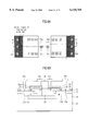
- FIG. 5A is a plan view of an SOI device according to a third embodiment of the present invention.
- FIG. 5B is a cross-sectional view showing a structure of the SOI device, taken along line of III--III of FIG. 5A;
- FIG. 6A is a plan view of an SOI device according to a fourth embodiment of the present invention.
- FIG. 6B is a cross-sectional view showing a structure of the SOI device, taken along line of IV--IV of FIG. 6A.
- FIG. 2A is a plan view of an SOI device according to the first embodiment of the present invention
- FIG. 2B is a cross-sectional view showing a structure of the SOI device, taken along line I--I of FIG. 2A
- FIGS. 3A to 3K are cross-sectional views showing process steps of a method for fabricating the SCI device, taken along line I--I of FIG. 2A
- FIG. 4A is a plan view showing an SOI device according to the second embodiment of the present invention
- FIG. 4B is a cross-sectional view showing a structure of the SOI device, taken along line II--II of FIG. 4A
- FIG. 5A is plan view of an SOI device according to the third embodiment of the present invention
- FIG. 5B is a cross-sectional view of a structure of the SOI device, taken along line of III--III of FIG. 5A
- FIG. 6A is a plan view of an SOI device according to the fourth embodiment of the present invention
- FIG. 6B is a cross-sectional view showing a structure of the SOI device, taken along line of IV--IV of FIG. 6A.
- a second buried oxide film 25 is formed on a second semiconductor substrate 24.
- p and n type heavily doped polysilicon layers 23a and 23b are formed on the second buried oxide film 25 and isolated from each other by an isolation oxide film 26 formed on the buried oxide film 25.
- First buried oxide films 22a are formed in the p and n type heavily doped polysilicon layers 23a and 23b to be spaced apart.
- a p type semiconductor layer 20b and a first active region are formed on the first buried oxide film 22a, spaced apart from the p type heavily doped polysilicon layer 23a.
- a first oxide film 21 is formed between the p type semiconductor layer 20b and the first active region.
- An n type semiconductor layer 20c and a second active region are formed on the first buried oxide film 22a, spaced apart from the n type heavily doped.
- a first oxide film 21 is formed between the n type semiconductor layer 20b and the second active region.
- a gate oxide film 29 and a first gate electrode 30a are successively formed on the first active region on the p type heavily doped polysilicon layer 23a.
- Source/drain regions 34a/34b are formed in the first active region at both sides of the first gate electrode 30a.
- a gate oxide film 29 and a second gate electrode 23b are successively formed on the second active region on the n type heavily doped polysilicon layer 23b.
- Source/drain region 32a/32b are formed in the second active region at both sides of the second gate electrode 39b.
- an interlayer insualting film 35 having contact holes on the p and n type semiconductor layers 20b and 20c and the source/drain regions 32a/32b and 34a/34b.
- Contact pads 36a and 36f and line layers 36b, 36c, 36d, and 36e are formed in the contact holes and on the interlayer insulating layer adjoining to the contact holes.
- the first and second active regions are connected to the p and n type semiconductor layers 20b and 20c through the p and n type polysilicon layers 23a and 23b, respectively.
- a second buried oxide film 25 is formed on a second semiconductor substrate 24 as shown in FIGS. 4A and 4B.
- p and n type heavily doped polysilicon layers 23a and 23b are formed on the second buried oxide film 25 and spaced apart from each other by an isolation oxide film 26.
- First buried oxide films 22 are formed in the p and n type heavily doped polysilicon layers 23a and 23b.
- These first buried oxide films 22 are under a contact pad 37a on the p type semiconductor layer 20a on the p type heavily doped polysilicon layer 23a and under portion of the source/drain region and a corner portion of the first gate electrode 30a.
- the first buried oxide films 22 are under a contact pad 37d on the n type semiconductor layer 20c on then type heavily doped polysilicon layer 23b and under portion of the source/drain region and a corner portion of the second gate electrode 30b.
- a p type semiocnductor layer 20b and a first active region are formed to spaced apart from each other on the first buried oxide films 22.
- a first oxide film 21 is formed between the p type semiconductor layer 20b and the first active region.
- An n type semiconductor layer 20c and a second active region are formed to be spaced apart from each other on the first buried oxide film 22.
- Another oxide film 21 is formed between the n type semiconductor layer 20b and the second active region.
- First and second gate electrodes 30a and 30b are formed to cross the first and second active regions, respectively.
- Source/drain regions are formed in the first and second active regions at both sides of the first and second gate electrodes 30a and 30b, respectively.
- an interlayer insulating film 35 having contact holes on the p type semiconductor layer 20b, the source/drain regions, and the first and second gate electrodes 30a and 30b.
- Contact pads 37a and 37d and line layers 37b and 37c are formed in the contact holes and on the interlayer insualting film 35 adjoining to the contact holes.
- the SOI device of the third embodiment shown in FIGS. 5A and 5B has an identical structure with that of the second embodiment except for etched portion of the first buried oxide film 22.
- a first buried oxide film 22 is etched under a p type semiconductor layer 20b under the contact pad 38a, under center portion of a source or drain region, and under center portion of a first gate electrtode 30a adjoining to the source or drain region, thereby forming first buried oxide films 22.
- a first buried oxide film 22 is etched under an n type semiconductor layer 20c under a contact pad 38d, under center portion of a source or drain region, and under center portion of a second gate electrode 30b adjoining to the source or drain region.
- the SOI device of the fourth embodiment shown in FIGS. 6A and 6B has an identical structure with that of the second embodiment except for etched portion of the first buried oxide film 22 and shapes of the first and second gate electrodes 30a and 30b.
- the first buried oxide film 22 is etched under a p type semiconductor layer 20b under a contact pad 39a, and under part of a first active region except a first gate electrode 30a and source/drain regions.
- the first buried oxide film 22 is etched under an n type semiconductor layer 20c under a contact pad 39d, and under part of a second active region except a second gate electrode 30b and source/drain regions.
- FIGS. 3A to 3K are cross-sectional views showing process steps of a method for fabricating an SOI device, taken along line I--I of FIG. 2A.
- a first semiconductor substrate 20 is etched by a predetermined depth to form a plurality of trenches. Subsequently, an oxide film is deposited on the first semiconductor substrate 20 including the trenches. Next, a CMP process is carried out so that formed is a first oxide film 21 filling the trenches. This oxide film 21 is 500-1500 Angstrom thick.
- a 500 ⁇ 3000 Angstrom thick first buried oxide film 22 is formed on the first semiconductor substrate 20 with a CVD process.
- a photoresist film is coated on the first buried oxide film 22 and patterned with an exposure and development process to expose predetermined areas of the first buried oxide film 22 between the trenches but not areas of the first film 22 for placements of CMOS transistors between the trenches.
- the first buried oxide film 22 is removed to expose the semiconductor substrate 20.
- a 2000 ⁇ 6000 Angstrom thick undoped polysilicon layer is deposited on the first buried oxide film 22 and the first semiconductor substrate 20 and then is subjected to an etch-back process or a CMP process, thus forming a 1000 ⁇ 2000 Angstrom thick undoped polysilicon layer 23.
- a 1000 ⁇ 4000 Angstrom thick second buried oxide film 25 is deposited on a second semiconductor substrate 24 with a CVD process or a thermal oxidation process.
- the undoped polysilicon layer 23 on the first semiconductor substrate 20 and the second buried oxide film 25 on the second semiconductor substrate 24 are heated them at a temperature of 850 ⁇ 1050° C. so that they are bonded to each other.
- the first semiconductor substrate 20 is polished with a CMP process for planarization until the first oxide film 21 is exposed.
- the difference between the etch rates of the first substrate 20 and the first oxide film 21 is used to polish the first substrate 20, and this first oxide film 21 serves as an etch stop.
- the semiconductor layers 20a between the first oxide films 21, the first buried oxide film 22, and the undoped polysilicon layer 23 are etched to form a trench isolation region.
- An oxide film is deposited on the first oxide film 21 and the semiconductor layer 20a and the trench isolation regions and planarized with a CMP process to form an isolation oxide film 26.
- a photoresist film 27 is coated on the first oxide film 21, the semiconductor layer 20a, and the isolation oxide film 26, and patterned with an exposure and development process to be removed at one whole side of the isolation oxide film 26.
- the patterned photoresist film 27 serving as a mask, boron ions having a concentration of 5E14 ⁇ 1E15 cm -2 are injected into the undoped polysilicon layer 23, which thus becomes a p type heavily doped polysilicon layer 23a.
- another photoresist film 28 is coated on the first oxide film 21, the semiconductor layer 20a, and the isolation oxide film 26, and patterned with an exposure and development process to be removed at the other side of the isolation oxide film 26.
- patterned photoresist film 28 serving as a mask, phosphorus ions having a concentration of 5E14 ⁇ 1E15 cm -2 are injected into the undoped polysilicon layer 23a, which thus becomes an n type heavily doped polysilicon layer 23b.
- an ion-implanting process for adjusting threshold voltage can be carried out after depositing p and n type polysilicon layers 23a and 23b.
- an oxide film and a silicon layer are deposited on the entire surface and anisotropically etched so that a gate oxide film 22 and a first gate electrode 30a for an NMOS transistor and a gate oxide film 22 and a second gate electrode 30b for a PMOS transistor are formed on the semiconductor layers 20a under which the first buried oxide film 22 is etched out.
- both the first and second gate electrodes 30a and 30b are made of n type doped polysilicon.
- the first and second gate electrodes 30a and 30b for NMOS and PMOS transistors, respectively are made of n type doped polysilicon and p type doped polysilicon, respectively.
- a metal layer or a metal silicide layer can be further formed on the first and second gate electrodes 30a and 30b.
- a photoresist film 31 is coated on the entire surface and patterned with an exposure and development process to expose the semiconductor layer 20a where the first gate electrode 30a is not formed in an area for an NMOS transistor and the semiconductor layer 20a at both sides of the second gate electrode 30b in an area of a PMOS transistor.
- boron ions of P type having a concentration of 1E15 ⁇ 5E15 cm -2 are injected to form source/drain regions 32a/32b in the p type semiconductor layer 20b.
- These source/drain regions 32a/32b have an LDD (lightly doped drain) structure.
- a photoresist film 33 is coated and patterned with an exposure and development process to expose the semiconductor layer 20a where the second gate electrode 30b is not formed in the PMOS transistor and the first gate electrode 30a and the semiconductor layer 20a at both sides of the gate electrode 30a.
- the patterned photoresist film 33 serving as a mask, n type As ions having a concentration of 1E15 ⁇ 5E15 cm -2 are injected so that an n type semiconductor layer 20c and source/drain regions 34a/34b having an LDD structure are formed.
- an interlayer insulating film 35 is deposited and removed to expose predetermined areas of the p and n type semiconductor layers 20b and 20c and predetermined areas of the p and n type source/drain regions 32a/32b and 34a/34b, thereby forming contact holes.
- a metal layer or a semiconductor layer is formed to fill the contact holes and anisotropically etched to form contact pads 36a and 36f on the p and n type semiconductor layers 20b and 20c, respectively, and line layers 36b, 36c, 36d, 36e on the n and p source/drain regions 32a/32b, and 34a/34b.
- the channel region of the NMOS transistor is connected to the contact pad 36a through the p type heavily doped polysilicon layer 23a and the p type semiconductor layer 20b, holes generated at the channel are not accumulated at the channel but drained to an outer terminal. Since the channel region of the PMOS transistor is connected to the contact pad 36f through the n type heavily doped polysilicon layer 23b and the n type semiconductor layer 20c, holes generated at the channel are not accumulated but drain to an outer terminal. Therefore, there is no floating body effect generated.
- the SOI device and the method for fabricating the same of the present invention have the following advantage.
- Channels of NMOS and PMOS transistors are designed to be electrically connected to contact pads, floating body effect is reduced, thereby enhancing the performance of a device.
Landscapes
- Engineering & Computer Science (AREA)
- Power Engineering (AREA)
- Microelectronics & Electronic Packaging (AREA)
- Physics & Mathematics (AREA)
- Condensed Matter Physics & Semiconductors (AREA)
- General Physics & Mathematics (AREA)
- Computer Hardware Design (AREA)
- Manufacturing & Machinery (AREA)
- Ceramic Engineering (AREA)
- Thin Film Transistor (AREA)
Abstract
Description
Claims (10)
Priority Applications (1)
Application Number | Priority Date | Filing Date | Title |
---|---|---|---|
US09/618,288 US6348715B1 (en) | 1997-12-15 | 2000-07-18 | SOI (silicon on insulator) device |
Applications Claiming Priority (2)
Application Number | Priority Date | Filing Date | Title |
---|---|---|---|
KR1019970068702A KR100281109B1 (en) | 1997-12-15 | 1997-12-15 | Silicon on insulator device and method for fabricating the same |
KR97-68702 | 1997-12-15 |
Related Child Applications (1)
Application Number | Title | Priority Date | Filing Date |
---|---|---|---|
US09/618,288 Division US6348715B1 (en) | 1997-12-15 | 2000-07-18 | SOI (silicon on insulator) device |
Publications (1)
Publication Number | Publication Date |
---|---|
US6110769A true US6110769A (en) | 2000-08-29 |
Family
ID=19527303
Family Applications (1)
Application Number | Title | Priority Date | Filing Date |
---|---|---|---|
US09/197,580 Expired - Fee Related US6110769A (en) | 1997-12-15 | 1998-11-23 | SOI (silicon on insulator) device and method for fabricating the same |
Country Status (4)
Country | Link |
---|---|
US (1) | US6110769A (en) |
JP (1) | JP3644833B2 (en) |
KR (1) | KR100281109B1 (en) |
DE (1) | DE19857059B4 (en) |
Cited By (21)
Publication number | Priority date | Publication date | Assignee | Title |
---|---|---|---|---|
US6294413B1 (en) | 2000-12-27 | 2001-09-25 | Vanguard International Semiconductor Corp. | Method for fabricating a SOI (silicon on insulator) device |
US6358820B1 (en) * | 2000-04-17 | 2002-03-19 | Mitsubishi Denki Kabushiki Kaisha | Method of manufacturing semiconductor device |
US6387739B1 (en) * | 1998-08-07 | 2002-05-14 | International Business Machines Corporation | Method and improved SOI body contact structure for transistors |
US6458638B2 (en) * | 1998-05-27 | 2002-10-01 | Samsung Electronics Co., Ltd. | Method for fabricating a semiconductor memory device having silicon-on-insulator (SOI) structure |
US6461903B2 (en) * | 2000-06-28 | 2002-10-08 | Hynix Semiconductor Inc. | Method for fabricating a part depletion type SOI device preventing a floating body effect |
US6528853B2 (en) * | 2000-01-05 | 2003-03-04 | International Business Machines Corporation | Method and semiconductor structure for implementing dual plane body contacts for silicon-on-insulator (SOI) transistors |
US6762477B2 (en) | 2000-03-24 | 2004-07-13 | Renesas Technology Corp. | Semiconductor device |
US6794716B2 (en) | 2000-08-11 | 2004-09-21 | Samsung Electronics Co., Ltd. | SOI MOSFET having body contact for preventing floating body effect and method of fabricating the same |
US20050151193A1 (en) * | 2004-01-08 | 2005-07-14 | International Business Machines Corporation | Discriminative soi with oxide holes underneath dc source/drain |
US20070069294A1 (en) * | 2005-09-29 | 2007-03-29 | International Business Machines Corporation | Stress engineering using dual pad nitride with selective soi device architecture |
US20100032796A1 (en) * | 2008-08-07 | 2010-02-11 | Brown Brennan J | Integrated Circuit Structure, Design Structure, and Method Having Improved Isolation and Harmonics |
WO2011008895A1 (en) * | 2009-07-15 | 2011-01-20 | Io Semiconductor | Semiconductor-on-insulator with back side body connection |
US20110012199A1 (en) * | 2009-07-15 | 2011-01-20 | Io Semiconductor, Inc. | Semiconductor-on-insulator with back side heat dissipation |
US20110012223A1 (en) * | 2009-07-15 | 2011-01-20 | Io Semiconductor, Inc. | Semiconductor-on-insulator with back side support layer |
US7927963B2 (en) | 2008-08-07 | 2011-04-19 | International Business Machines Corporation | Integrated circuit structure, design structure, and method having improved isolation and harmonics |
US8912646B2 (en) | 2009-07-15 | 2014-12-16 | Silanna Semiconductor U.S.A., Inc. | Integrated circuit assembly and method of making |
US8981488B1 (en) * | 2013-11-06 | 2015-03-17 | United Microelectronics Corp. | Semiconductor structure and integrated circuit |
US9390974B2 (en) | 2012-12-21 | 2016-07-12 | Qualcomm Incorporated | Back-to-back stacked integrated circuit assembly and method of making |
US9466719B2 (en) | 2009-07-15 | 2016-10-11 | Qualcomm Incorporated | Semiconductor-on-insulator with back side strain topology |
US9496227B2 (en) | 2009-07-15 | 2016-11-15 | Qualcomm Incorporated | Semiconductor-on-insulator with back side support layer |
US9515181B2 (en) | 2014-08-06 | 2016-12-06 | Qualcomm Incorporated | Semiconductor device with self-aligned back side features |
Families Citing this family (9)
Publication number | Priority date | Publication date | Assignee | Title |
---|---|---|---|---|
KR100324938B1 (en) * | 1999-12-29 | 2002-02-28 | 박종섭 | Method for fabricating pbsoi wafer using a epitaxy lateral overgrowth process |
KR100374554B1 (en) * | 2000-09-22 | 2003-03-04 | 주식회사 하이닉스반도체 | Structure of body-substrate contact for soi semiconductor device and method for fabricating the same |
JP4031986B2 (en) | 2000-11-22 | 2008-01-09 | アーファウエル リスト ゲゼルシャフト ミット ベシュレンクテル ハフツング | Method for supplying conditioned combustion gas to an internal combustion engine, apparatus for carrying out the method, method for measuring the amount of harmful substances in the exhaust gas of an internal combustion engine, and apparatus for carrying out the method |
KR100363555B1 (en) * | 2001-02-07 | 2002-12-05 | 삼성전자 주식회사 | An SOI semiconductor integrated circuit for eliminating floating body effects in SOI MOSFETs and method of fabricating the same |
KR100393218B1 (en) * | 2001-03-12 | 2003-07-31 | 삼성전자주식회사 | Semiconductor device having a silicon on insulator structure and method for fabricating the same |
US7416927B2 (en) | 2002-03-26 | 2008-08-26 | Infineon Technologies Ag | Method for producing an SOI field effect transistor |
DE10213545B4 (en) * | 2002-03-26 | 2006-06-08 | Infineon Technologies Ag | Method for producing an SOI field effect transistor and SOI field effect transistor |
DE10343132B4 (en) * | 2003-09-18 | 2009-07-09 | X-Fab Semiconductor Foundries Ag | Isolated MOS transistors with extended drain region for increased voltages |
CN109524355B (en) * | 2018-10-30 | 2020-11-10 | 上海集成电路研发中心有限公司 | Structure and forming method of semiconductor device |
Citations (6)
Publication number | Priority date | Publication date | Assignee | Title |
---|---|---|---|---|
US4970175A (en) * | 1988-08-09 | 1990-11-13 | U.S. Philips Corporation | Method of manufacturing a semiconductor device using SEG and a transitory substrate |
US5091330A (en) * | 1990-12-28 | 1992-02-25 | Motorola, Inc. | Method of fabricating a dielectric isolated area |
US5260233A (en) * | 1992-11-06 | 1993-11-09 | International Business Machines Corporation | Semiconductor device and wafer structure having a planar buried interconnect by wafer bonding |
US5521399A (en) * | 1992-06-17 | 1996-05-28 | International Business Machines Corporation | Advanced silicon on oxide semiconductor device structure for BiCMOS integrated circuit |
US5528054A (en) * | 1991-10-17 | 1996-06-18 | Mitsubishi Denki Kabushiki Kaisha | Semiconductor device having active region in semiconductor layer on insulator layer and manufacturing method thereof |
US5597739A (en) * | 1994-01-19 | 1997-01-28 | Sony Corporation | MOS transistor and method for making the same |
Family Cites Families (1)
Publication number | Priority date | Publication date | Assignee | Title |
---|---|---|---|---|
KR970052023A (en) * | 1995-12-30 | 1997-07-29 | 김주용 | S-O I device and its manufacturing method |
-
1997
- 1997-12-15 KR KR1019970068702A patent/KR100281109B1/en not_active IP Right Cessation
-
1998
- 1998-11-23 US US09/197,580 patent/US6110769A/en not_active Expired - Fee Related
- 1998-12-10 DE DE19857059A patent/DE19857059B4/en not_active Expired - Fee Related
- 1998-12-15 JP JP35591998A patent/JP3644833B2/en not_active Expired - Fee Related
Patent Citations (6)
Publication number | Priority date | Publication date | Assignee | Title |
---|---|---|---|---|
US4970175A (en) * | 1988-08-09 | 1990-11-13 | U.S. Philips Corporation | Method of manufacturing a semiconductor device using SEG and a transitory substrate |
US5091330A (en) * | 1990-12-28 | 1992-02-25 | Motorola, Inc. | Method of fabricating a dielectric isolated area |
US5528054A (en) * | 1991-10-17 | 1996-06-18 | Mitsubishi Denki Kabushiki Kaisha | Semiconductor device having active region in semiconductor layer on insulator layer and manufacturing method thereof |
US5521399A (en) * | 1992-06-17 | 1996-05-28 | International Business Machines Corporation | Advanced silicon on oxide semiconductor device structure for BiCMOS integrated circuit |
US5260233A (en) * | 1992-11-06 | 1993-11-09 | International Business Machines Corporation | Semiconductor device and wafer structure having a planar buried interconnect by wafer bonding |
US5597739A (en) * | 1994-01-19 | 1997-01-28 | Sony Corporation | MOS transistor and method for making the same |
Non-Patent Citations (4)
Title |
---|
H.F. Wei et al., International Electron Devices Meeting 1993 (IEDM 93), pp. 739 742. * |
H.F. Wei et al., International Electron Devices Meeting 1993 (IEDM 93), pp. 739-742. |
Terukazu Ohno et al., International Electron Devices Meeting 1995(IEDM 95), pp. 627 630. * |
Terukazu Ohno et al., International Electron Devices Meeting 1995(IEDM 95), pp. 627-630. |
Cited By (39)
Publication number | Priority date | Publication date | Assignee | Title |
---|---|---|---|---|
US6458638B2 (en) * | 1998-05-27 | 2002-10-01 | Samsung Electronics Co., Ltd. | Method for fabricating a semiconductor memory device having silicon-on-insulator (SOI) structure |
US6387739B1 (en) * | 1998-08-07 | 2002-05-14 | International Business Machines Corporation | Method and improved SOI body contact structure for transistors |
US6528853B2 (en) * | 2000-01-05 | 2003-03-04 | International Business Machines Corporation | Method and semiconductor structure for implementing dual plane body contacts for silicon-on-insulator (SOI) transistors |
US6762477B2 (en) | 2000-03-24 | 2004-07-13 | Renesas Technology Corp. | Semiconductor device |
US6358820B1 (en) * | 2000-04-17 | 2002-03-19 | Mitsubishi Denki Kabushiki Kaisha | Method of manufacturing semiconductor device |
US6461903B2 (en) * | 2000-06-28 | 2002-10-08 | Hynix Semiconductor Inc. | Method for fabricating a part depletion type SOI device preventing a floating body effect |
US6794716B2 (en) | 2000-08-11 | 2004-09-21 | Samsung Electronics Co., Ltd. | SOI MOSFET having body contact for preventing floating body effect and method of fabricating the same |
US6294413B1 (en) | 2000-12-27 | 2001-09-25 | Vanguard International Semiconductor Corp. | Method for fabricating a SOI (silicon on insulator) device |
US20050151193A1 (en) * | 2004-01-08 | 2005-07-14 | International Business Machines Corporation | Discriminative soi with oxide holes underneath dc source/drain |
US6958516B2 (en) * | 2004-01-08 | 2005-10-25 | International Business Machines Corporation | Discriminative SOI with oxide holes underneath DC source/drain |
US20070069294A1 (en) * | 2005-09-29 | 2007-03-29 | International Business Machines Corporation | Stress engineering using dual pad nitride with selective soi device architecture |
US7202513B1 (en) * | 2005-09-29 | 2007-04-10 | International Business Machines Corporation | Stress engineering using dual pad nitride with selective SOI device architecture |
US20070122965A1 (en) * | 2005-09-29 | 2007-05-31 | International Business Machines Corporation | Stress engineering using dual pad nitride with selective soi device architecture |
CN100464425C (en) * | 2005-09-29 | 2009-02-25 | 国际商业机器公司 | Semiconductor constructions and manufacturing method thereof |
US7550364B2 (en) | 2005-09-29 | 2009-06-23 | International Business Machines Corporation | Stress engineering using dual pad nitride with selective SOI device architecture |
US20100032796A1 (en) * | 2008-08-07 | 2010-02-11 | Brown Brennan J | Integrated Circuit Structure, Design Structure, and Method Having Improved Isolation and Harmonics |
US7804151B2 (en) * | 2008-08-07 | 2010-09-28 | International Business Machines Corporation | Integrated circuit structure, design structure, and method having improved isolation and harmonics |
US7927963B2 (en) | 2008-08-07 | 2011-04-19 | International Business Machines Corporation | Integrated circuit structure, design structure, and method having improved isolation and harmonics |
US20110012199A1 (en) * | 2009-07-15 | 2011-01-20 | Io Semiconductor, Inc. | Semiconductor-on-insulator with back side heat dissipation |
US9034732B2 (en) | 2009-07-15 | 2015-05-19 | Silanna Semiconductor U.S.A., Inc. | Semiconductor-on-insulator with back side support layer |
US20110012223A1 (en) * | 2009-07-15 | 2011-01-20 | Io Semiconductor, Inc. | Semiconductor-on-insulator with back side support layer |
WO2011008895A1 (en) * | 2009-07-15 | 2011-01-20 | Io Semiconductor | Semiconductor-on-insulator with back side body connection |
US8232597B2 (en) | 2009-07-15 | 2012-07-31 | Io Semiconductor, Inc. | Semiconductor-on-insulator with back side connection |
US8357975B2 (en) | 2009-07-15 | 2013-01-22 | Io Semiconductor, Inc. | Semiconductor-on-insulator with back side connection |
US8859347B2 (en) | 2009-07-15 | 2014-10-14 | Silanna Semiconductor U.S.A., Inc. | Semiconductor-on-insulator with back side body connection |
US8912646B2 (en) | 2009-07-15 | 2014-12-16 | Silanna Semiconductor U.S.A., Inc. | Integrated circuit assembly and method of making |
US8921168B2 (en) | 2009-07-15 | 2014-12-30 | Silanna Semiconductor U.S.A., Inc. | Thin integrated circuit chip-on-board assembly and method of making |
US10217822B2 (en) | 2009-07-15 | 2019-02-26 | Qualcomm Incorporated | Semiconductor-on-insulator with back side heat dissipation |
US9029201B2 (en) | 2009-07-15 | 2015-05-12 | Silanna Semiconductor U.S.A., Inc. | Semiconductor-on-insulator with back side heat dissipation |
US20110012669A1 (en) * | 2009-07-15 | 2011-01-20 | Io Semiconductor, Inc. | Semiconductor-on-insulator with back side connection |
US9368468B2 (en) | 2009-07-15 | 2016-06-14 | Qualcomm Switch Corp. | Thin integrated circuit chip-on-board assembly |
US9748272B2 (en) | 2009-07-15 | 2017-08-29 | Qualcomm Incorporated | Semiconductor-on-insulator with back side strain inducing material |
US9412644B2 (en) | 2009-07-15 | 2016-08-09 | Qualcomm Incorporated | Integrated circuit assembly and method of making |
US9466719B2 (en) | 2009-07-15 | 2016-10-11 | Qualcomm Incorporated | Semiconductor-on-insulator with back side strain topology |
US9496227B2 (en) | 2009-07-15 | 2016-11-15 | Qualcomm Incorporated | Semiconductor-on-insulator with back side support layer |
US9576937B2 (en) | 2012-12-21 | 2017-02-21 | Qualcomm Incorporated | Back-to-back stacked integrated circuit assembly |
US9390974B2 (en) | 2012-12-21 | 2016-07-12 | Qualcomm Incorporated | Back-to-back stacked integrated circuit assembly and method of making |
US8981488B1 (en) * | 2013-11-06 | 2015-03-17 | United Microelectronics Corp. | Semiconductor structure and integrated circuit |
US9515181B2 (en) | 2014-08-06 | 2016-12-06 | Qualcomm Incorporated | Semiconductor device with self-aligned back side features |
Also Published As
Publication number | Publication date |
---|---|
JPH11243211A (en) | 1999-09-07 |
KR100281109B1 (en) | 2001-03-02 |
DE19857059B4 (en) | 2005-04-21 |
KR19990049707A (en) | 1999-07-05 |
JP3644833B2 (en) | 2005-05-11 |
DE19857059A1 (en) | 1999-06-24 |
Similar Documents
Publication | Publication Date | Title |
---|---|---|
US6110769A (en) | SOI (silicon on insulator) device and method for fabricating the same | |
KR100189966B1 (en) | Mos transistor of soi structure and method for manufacturing the same | |
US5620912A (en) | Method of manufacturing a semiconductor device using a spacer | |
US7741673B2 (en) | Floating body memory and method of fabricating the same | |
US6593192B2 (en) | Method of forming a dual-gated semiconductor-on-insulator device | |
US7285456B2 (en) | Method of fabricating a fin field effect transistor having a plurality of protruding channels | |
US6271065B1 (en) | Method directed to the manufacture of an SOI device | |
WO2006039600A1 (en) | Independently accessed double-gate and tri-gate transistors in same process flow | |
JP3857622B2 (en) | Semiconductor device and manufacturing method thereof | |
JP4832629B2 (en) | Semiconductor device | |
KR20030050995A (en) | Method for fabricating high-integrated transistor | |
JP2000196069A (en) | Insulated gate field-effect transistor and semiconductor body, and method of forming field-effect transistor, and method of forming semiconductor body | |
US11967626B2 (en) | Field effect transistors with gate fins and method of making the same | |
US6410973B2 (en) | Thin film SOI MOSFET | |
US6225661B1 (en) | MOS transistor with stepped gate insulator | |
US6844224B2 (en) | Substrate contact in SOI and method therefor | |
US6348715B1 (en) | SOI (silicon on insulator) device | |
US11437512B2 (en) | Buried channel metal-oxide-semiconductor field-effect transistor (MOSFET) and forming method thereof | |
KR100506455B1 (en) | A method for forming a semiconductor device | |
CN113643981B (en) | Manufacturing method of semi-floating gate transistor with bimetallic control gate | |
US12015084B2 (en) | Field effect transistors with gate fins and method of making the same | |
US11114442B2 (en) | Semiconductor memory device with shallow buried capacitor and fabrication method thereof | |
US6150276A (en) | Method for fabricating metal-oxide semiconductor transistor | |
KR100448090B1 (en) | Method for fabricating high-performance semiconductor device by reducing junction capacitance | |
KR20040009383A (en) | Semiconductor memory device having stacked capacitor and trench capacitor, and method for fabricating the same |
Legal Events
Date | Code | Title | Description |
---|---|---|---|
AS | Assignment |
Owner name: LG SEMICON CO., LTD., KOREA, REPUBLIC OF Free format text: ASSIGNMENT OF ASSIGNORS INTEREST;ASSIGNOR:SON, JEONG HWAN;REEL/FRAME:009628/0347 Effective date: 19981028 |
|
FEPP | Fee payment procedure |
Free format text: PAYOR NUMBER ASSIGNED (ORIGINAL EVENT CODE: ASPN); ENTITY STATUS OF PATENT OWNER: LARGE ENTITY |
|
FPAY | Fee payment |
Year of fee payment: 4 |
|
FPAY | Fee payment |
Year of fee payment: 8 |
|
FEPP | Fee payment procedure |
Free format text: PAYER NUMBER DE-ASSIGNED (ORIGINAL EVENT CODE: RMPN); ENTITY STATUS OF PATENT OWNER: LARGE ENTITY Free format text: PAYOR NUMBER ASSIGNED (ORIGINAL EVENT CODE: ASPN); ENTITY STATUS OF PATENT OWNER: LARGE ENTITY |
|
REMI | Maintenance fee reminder mailed | ||
LAPS | Lapse for failure to pay maintenance fees | ||
STCH | Information on status: patent discontinuation |
Free format text: PATENT EXPIRED DUE TO NONPAYMENT OF MAINTENANCE FEES UNDER 37 CFR 1.362 |
|
FP | Lapsed due to failure to pay maintenance fee |
Effective date: 20120829 |