US6066923A - Plasma display panel and method of driving plasma display panel - Google Patents
Plasma display panel and method of driving plasma display panel Download PDFInfo
- Publication number
- US6066923A US6066923A US09/158,003 US15800398A US6066923A US 6066923 A US6066923 A US 6066923A US 15800398 A US15800398 A US 15800398A US 6066923 A US6066923 A US 6066923A
- Authority
- US
- United States
- Prior art keywords
- scan
- electrodes
- sustaining
- period
- data
- Prior art date
- Legal status (The legal status is an assumption and is not a legal conclusion. Google has not performed a legal analysis and makes no representation as to the accuracy of the status listed.)
- Expired - Lifetime
Links
Images


Classifications
-
- G—PHYSICS
- G09—EDUCATION; CRYPTOGRAPHY; DISPLAY; ADVERTISING; SEALS
- G09G—ARRANGEMENTS OR CIRCUITS FOR CONTROL OF INDICATING DEVICES USING STATIC MEANS TO PRESENT VARIABLE INFORMATION
- G09G3/00—Control arrangements or circuits, of interest only in connection with visual indicators other than cathode-ray tubes
- G09G3/20—Control arrangements or circuits, of interest only in connection with visual indicators other than cathode-ray tubes for presentation of an assembly of a number of characters, e.g. a page, by composing the assembly by combination of individual elements arranged in a matrix no fixed position being assigned to or needed to be assigned to the individual characters or partial characters
- G09G3/22—Control arrangements or circuits, of interest only in connection with visual indicators other than cathode-ray tubes for presentation of an assembly of a number of characters, e.g. a page, by composing the assembly by combination of individual elements arranged in a matrix no fixed position being assigned to or needed to be assigned to the individual characters or partial characters using controlled light sources
- G09G3/28—Control arrangements or circuits, of interest only in connection with visual indicators other than cathode-ray tubes for presentation of an assembly of a number of characters, e.g. a page, by composing the assembly by combination of individual elements arranged in a matrix no fixed position being assigned to or needed to be assigned to the individual characters or partial characters using controlled light sources using luminous gas-discharge panels, e.g. plasma panels
- G09G3/288—Control arrangements or circuits, of interest only in connection with visual indicators other than cathode-ray tubes for presentation of an assembly of a number of characters, e.g. a page, by composing the assembly by combination of individual elements arranged in a matrix no fixed position being assigned to or needed to be assigned to the individual characters or partial characters using controlled light sources using luminous gas-discharge panels, e.g. plasma panels using AC panels
- G09G3/291—Control arrangements or circuits, of interest only in connection with visual indicators other than cathode-ray tubes for presentation of an assembly of a number of characters, e.g. a page, by composing the assembly by combination of individual elements arranged in a matrix no fixed position being assigned to or needed to be assigned to the individual characters or partial characters using controlled light sources using luminous gas-discharge panels, e.g. plasma panels using AC panels controlling the gas discharge to control a cell condition, e.g. by means of specific pulse shapes
- G09G3/293—Control arrangements or circuits, of interest only in connection with visual indicators other than cathode-ray tubes for presentation of an assembly of a number of characters, e.g. a page, by composing the assembly by combination of individual elements arranged in a matrix no fixed position being assigned to or needed to be assigned to the individual characters or partial characters using controlled light sources using luminous gas-discharge panels, e.g. plasma panels using AC panels controlling the gas discharge to control a cell condition, e.g. by means of specific pulse shapes for address discharge
- G09G3/2932—Addressed by writing selected cells that are in an OFF state
-
- G—PHYSICS
- G09—EDUCATION; CRYPTOGRAPHY; DISPLAY; ADVERTISING; SEALS
- G09G—ARRANGEMENTS OR CIRCUITS FOR CONTROL OF INDICATING DEVICES USING STATIC MEANS TO PRESENT VARIABLE INFORMATION
- G09G2310/00—Command of the display device
- G09G2310/02—Addressing, scanning or driving the display screen or processing steps related thereto
- G09G2310/0202—Addressing of scan or signal lines
- G09G2310/0218—Addressing of scan or signal lines with collection of electrodes in groups for n-dimensional addressing
-
- G—PHYSICS
- G09—EDUCATION; CRYPTOGRAPHY; DISPLAY; ADVERTISING; SEALS
- G09G—ARRANGEMENTS OR CIRCUITS FOR CONTROL OF INDICATING DEVICES USING STATIC MEANS TO PRESENT VARIABLE INFORMATION
- G09G2310/00—Command of the display device
- G09G2310/02—Addressing, scanning or driving the display screen or processing steps related thereto
- G09G2310/0202—Addressing of scan or signal lines
- G09G2310/0221—Addressing of scan or signal lines with use of split matrices
Definitions
- the present invention relates to methods of driving plasma display panels and, more particularly, to methods of driving AC discharge plasma display panels having electrodes covered by a dielectric and operable in indirect AC discharge state.
- the plasma display panel (hereinafter referred to as PDP) usually has many advantages, such as having a thin structure, being free from flicker, having a large contrast ratio, being capable of relatively readily providing a large display area, being able to provide fast response, and being of self light emission type to permit multiple color light emission by utilizing phosphors. Owing to these advantages, the PDP is recently finding wide-spread applications to the fields of displays concerning computers and color image displays.
- the AC discharge PDPs are classified depending on their operating system into an AC discharge type having electrodes covered by a dielectric and operable in an indirect AC discharge state, and a DC discharge type having electrodes exposed to a discharge space and operable in a DC discharge state.
- the AC discharge PDPs have advantages in eliminating spattering of electrodes due to discharge and long life.
- the AC PDPs are further classified depending on the drive system into a memory type which utilizes a discharge cell memory, and a refresh type which does not utilize any such memory.
- the PDP light intensity is proportional to the number of discharge times, i.e., the number of repeated pulse voltage applications.
- the refresh type PDP the light intensity is reduced with increasing display capacity. Therefore, this type is adopted for only small discharge capacity PDPs.
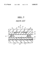
- FIG. 7 is a sectional view showing an example of the AC discharge memory type PDP.
- this PDP comprises a rear and a front insulating substrate 1 and 2 of glass, a scan and a sustaining electrode 3 and 4, which are transparent and formed at a predetermined spacing therebetween on the substrate 2 and constitute each of a plurality of parallel electrode sets, tracing electrodes 5 and 6 formed on the scan and sustaining electrodes 3 and 4 for reducing the electrode resistance thereof, a dielectric layer 12 covering the scan, sustaining and tracing electrodes 3 to 6, a protective layer 13 of magnesium oxide or like material laminated on the dielectric layer 12 for protecting the same layer 12 from discharge, a plurality of parallel data electrodes 7 (only one thereof being shown) formed on the substrate 1 such as to cross the scan and sustaining electrodes 3 and 4, a dielectric layer 14 covering the data electrodes 7, a plurality of discharge gas spaces 8 (only one thereof being shown) formed between the substrates 1 and 2 and filled with discharge gas, e.g., of helium, neon, xenon, etc.
- discharge gas e.g., of helium, neon
- a partitioning wall member 9 provided on the dielectric layer 14 to form the discharge gas spaces 8 and define display cells, and phosphor 11 coated on the dielectric layer 14 and also on the side wall surfaces of the partitioning wall member 9 for converting ultraviolet rays generated with discharge of the discharge gas filled in the discharge gas spaces 8 to visible light 11.
- the actual PDP for instance a VGA panel, has a cell pixel matrix on the display area, having 480 rows or lines and 1,920 columns of display cells or pixels like those noted above, 480 scan electrodes 3 and the same number of sustaining electrodes 4, and 1,920 data electrodes 7.
- the data electrode pitch is 0.35 mm
- the scan electrode pitch is 1.05 mm.
- the scan electrodes are at a distance of 0.2 mm from the data electrodes, and the scan and sustaining electrodes 3 and 4 in each electrode set are spaced apart by 0.1 mm.
- a sustaining pulse which is a pulse voltage of the same polarity as the wall voltage
- the wall voltage is superimposed as effective voltage on the sustaining pulse.
- the discharge thus can be sustained by continuously applying the sustaining pulse between the scan and sustaining electrodes 3 and 4.
- the sustained discharge can be de-sustained by applying, to the scan or sustaining electrode 3 or 4, an erasing pulse, which is a wide low voltage pulse or a narrow pulse with a level of the order of the sustaining pulse voltage such as to neutralize or cancel the wall voltage.
- an erasing pulse which is a wide low voltage pulse or a narrow pulse with a level of the order of the sustaining pulse voltage such as to neutralize or cancel the wall voltage.
- FIG. 8 is a schematic plan view showing the PDP having the display cell matrix array as shown in FIG. 7.
- the PDP 15 is a dot matrix display panel having display cells 16 in a dot matrix array of j rows and k columns.
- the PDP has parallel scan electrodes S c1 , S c2 , . . . , S cj and sustaining electrodes S u1 , S u2 , . . . , S uj and as column electrodes it has data electrodes D 1 , D 2 , . . . , D k crossing the scan and sustaining electrodes.
- FIG. 9 is a waveform chart showing a prior art example of drive pulses for driving the PDP shown in FIG. 8. This example is proposed in Society for Information Display International Symposium Digest of Technical Papers, Vol. XXVI, 1995, pp. 807-810.
- labeled W u is a sustaining electrode drive voltage waveform applied commonly to the sustaining electrodes S u1 , S u2 , . . . S uj .
- Labeled W s1 , W s2 , . . . W sj are scan electrode drive voltage waveforms applied to the scan electrodes S c1 , S c2 , . . . , S cj , respectively.
- Labeled W d is a data electrode drive voltage waveform applied to the data electrode D i (123 i ⁇ k).
- the PDP drive cycle consists of a priming discharge period A, a writing discharge period B and a sustaining period C. Desired image display can be obtained with repeated discharge in these periods.
- priming discharge period A active particles and wall charge are generated in each discharge gas space 8 (see FIG. 7) in order to obtain stable writing discharge characteristics in the writing discharge period B.
- a priming discharge pulse P p is first applied to the sustaining electrodes to simultaneously cause discharge in all the display cells of the PDP 15.
- a priming discharge erase pulse P pe is simultaneously applied to all the scan electrodes to remove or reduce those charge parts of the wall charge generated in this period which impede the writing discharge and the sustained discharge.
- the priming discharge pulse P p is first applied to the sustaining electrodes S u1 , S u2 , . . . , S uj cause discharge in all the cells, and then the priming discharge erase pulse P pe is applied to the scan electrodes S c1 , S c2 , . . . , S cj to bring about erase discharge for erasing the charge parts of the charge deposited by the priming discharge pulse P p which impede the writing discharge and the sustained discharge.
- a scan base pulse P b is first applied to all the scan electrodes S c1 , S c2 , . . . , S cj . Then, successive scan pulses P w are applied to the scan electrodes S c1 , S c2 , . . . , S cj , and in synchronism to the scan pulses P w data pulses Pd are selectively applied to the data electrodes D i (1 ⁇ i ⁇ k) in the display cells to be driven for display.
- writing discharge is caused to generate wall charge in the cells to be driven.
- the scan base pulse P b By applying the scan base pulse P b , it is possible to reduce the level of the scan base pulse P w , thus reducing the maximum working voltage level of a high break-down voltage IC which generates the scan pulses P w and reducing the cost of the drive IC, when the level of the scan pulses P w is high, the rising of the scan pulse P w causes undesired discharge tending to de-sustain the writing discharge, which is brought about by the scan and data pulses. By applying the scan base pulse P b , the level of the scan pulse P w can be reduced to eliminate the undesired discharge.
- a sustaining pulse P u is applied to the sustaining electrodes, while applying a sustaining pulse P s lagging in phase by 180 degrees behind the sustaining pulse P u to each scan electrode, thus sustaining discharge necessary to obtain a desired light intensity in the display cells, in which the writing discharge was brought about in the writing discharge period B.
- the gradation display is obtained by controlling the number of times by which to cause light emission.
- a sub-field method as will be described in the following is used for high light intensity gradation display.
- FIG. 10 is a view for describing the sub-field method.
- the ordinate is taken for the scan electrode column, and the abscissa is taken for time.
- One frame image is set during one filed as shown in FIG. 10.
- One field is largely set to be in a range of 1/47 to 1/76 second, although it varies with computers and broadcasting systems.
- the light intensity of emission in each pixel in each sub-field is controlled by weight multiplying the number of times of sustained discharge light emission in the pixel by 2 n , and is given as: ##EQU1##
- n is sub-field number, being “1” for the lowest light intensity sub-field and "k” for the highest light intensity sub-field.
- L 1 is the light intensity of the lowest light intensity sub-field.
- a n is a variable having value of either “1” or “0” and being “1” when driving pertinent pixels in the n-th sub-field for light emission and "0” otherwise. Since the light intensity of emission varies with the sub-fields, the light intensity can be controlled by selecting "on” and "off” states in each field.
- the sub-fields shown in FIG. 10 have different time lengths. This is so because the number of times of the sustained discharge, i.e., the number of applied sustaining pulses P u and P n , is different with different sub-fields.
- the PDP its electrodes are formed on insulating substrate of glass and covered by glass graze, which is a dielectric constituted by glass paste. For this reason, a phenomenon called electromigration takes place, which is the precipitation of a glass graze component on the electrode surface due to an effective DC bias applied between the scan and sustaining electrodes.
- effective DC bias is meant not a purely DC bias but a voltage deviation in the integration of the voltage applied between the scan and sustaining electrodes over one drive cycle.
- FIG. 11 is a view showing an example of voltage waveforms, which brings about the electromigration.
- This DC bias brings about electromigration, i.e., migration of ions in the direction of the electric field.
- projections like tree branches grow between the scan and sustaining electrodes, and ultimately cause short-circuit thereof with one another.
- the projections grown thereon are of a conductive material, and increase the effective electrode area. This means that the effective discharge gap between the scan and sustaining electrodes is reduced.
- Such effective discharge gap reduction extremely reduces the initial discharge voltage in a short period of time. That is, even when a voltage which permits normal image display is initially set, erroneous "on" pixels are caused in a short period display operation. This erroneous "on” pixels disable maintaining normal display operation.
- FIG. 12 is a view showing an example of drive waveforms for preventing the electromigration.
- a priming discharge period at B a writing discharge period, at C a sustaining period, at P p a priming discharge pulse, at P b a scan base pulse, at P w scan pulses, at P x a pulse of voltage of 50 V, at P u sustaining electrode side sustaining pulses, and P s scan electrode side sustaining pulses.
- the last one is continued into a pause period. This last pulse cancels a DC voltage that is applied between the scan and sustaining electrodes in the writing discharge period B.
- the pause period should be set to be equal in time length to the writing discharge period.
- the pause period may not always be set to be equal to the writing discharge period
- the pause period may be set to be equal to the writing discharge period with a sacrifice in the sustaining period. In such a case, the result may be the failure of obtaining sufficient light intensity.
- This prior art method has another problem.
- the voltage of the last sustaining pulse applied to the scan electrode side is different from the voltage applied between the scan and sustaining electrodes in the writing discharge period.
- the effect of electromigration varies non-linearly with respect to the last applied sustaining pulse voltage. Therefore, it is difficult to determine the level and pulse length of the compensation pulse voltage, which is applied to the scan electrode side during the pause period in order to perfectly cancel the DC bias voltage in the writing discharge period.
- the present invention was made in view of the above problems inherent in the prior art, and it has an object of providing a method of driving a plasma display panel, which is free from reduction of the light intensity of emission due to sustaining period sacrifice, while suppressing reduction of the initial discharge voltage due to tree-branch-like projections precipitated between the scan and sustaining electrodes as a result of electromigration.
- a method of driving the plasma display panel in a plasma display comprising a plurality of scan electrodes provided on an insulating substrate, sustaining electrodes provided on the same insulating substrate such as to be paired with the scan electrodes, respectively, and parallel with the same, and a plurality of data electrodes provided on an insulating substrate facing the scan and sustaining electrodes such as to cross the same, data voltage corresponding to display data being supplied to the data electrodes, the method of driving the plasma display panel, in which display data is written in display cells by applying scan pulses to the scan electrodes during a scan period, during which a scan base pulse of a constant voltage is applied to the scan electrodes, comprising the steps of:
- the plurality of scan electrodes are divided into two scan electrode groups at the center of the electrode array in the scan direction thereof.
- the plurality of scan electrodes are divided into two scan electrode groups each constituted by every other scan electrodes in the scan direction.
- a method of driving the plasma display panel in a plasma display comprising a plurality of scan electrodes provided on an insulating substrate, sustaining electrodes provided on the same insulating substrate such as to be paired with the scan electrodes, respectively, and parallel with the same, and a plurality of data electrodes provided on an insulating substrate facing the scan and sustaining electrodes such as to cross the same, data voltage corresponding to display data being supplied to the data electrodes, the method of driving the plasma display panel, in which display data is written in display cells by applying scan pulses to the scan electrodes during a scan period, during which a scan base pulse of a constant voltage is applied to the scan electrodes, comprising the steps of:
- a plasma display comprising a plurality of scan electrodes provided on an insulating substrate, sustaining electrodes provided on the same insulating substrate such as to be paired with the scan electrodes, respectively, and parallel with the same, and a plurality of data electrodes provided on an insulating substrate facing the scan and sustaining electrodes such as to cross the same, data voltage corresponding to display data being supplied to the data electrodes, display data being written in display cells by applying scan pulses to the scan electrodes during a scan period, during which a scan base pulse of a constant voltage is applied to the scan electrodes, wherein the plurality of scan electrodes are divided into a plurality of scan electrode groups having different scan periods; and a compensation pulse voltage is applied to the scan electrodes in the scan electrode groups, which are in the non-scan periods during a writing discharge period of writing the display data in the display cells, to make up for a potential deviation generated between the scan and sustaining electrodes during the scan period.
- a plasma display comprising a plurality of scan electrodes provided on an insulating substrate, sustaining electrodes provided on the same insulating substrate such as to be paired with the scan electrodes, respectively, and parallel with the same, and a plurality of data electrodes provided on an insulating substrate facing the scan and sustaining electrodes such as to cross the same, data voltage corresponding to display data being supplied to the data electrodes, display data being written in display cells by applying scan pulses to the scan electrodes during a scan period, during which a scan base pulse of a constant voltage is applied to the scan electrodes, wherein the pluralities of scan and sustaining electrodes are divided into a plurality of scan and sustaining electrode groups having different scan periods; and a compensation pulse voltage is applied to the scan and sustaining electrodes in the scan and sustaining electrode groups, which are in the non-scan periods during a writing discharge period of writing the display data in the display cells, to make up for a potential deviation generated between the scan and sustaining electrodes during
- the tree-branch-like projection generation reaction is usually a reversible reaction.
- the generation of tree-branch-like projections can be prevented by applying an equivalent and opposite polarity DC bias.
- the scan electrodes are divided into a plurality of groups having either a scan or a non-scan period during the writing discharge period, and a compensation pulse is applied, without application of any scan base pulse, to the scan electrodes in the non-scan period.
- a compensation pulse is applied, without application of any scan base pulse, to the scan electrodes in the non-scan period.
- the sustaining period is not sacrificed.
- FIG. 1 is a waveform chart showing drive pulses for describing a first embodiment of the PDP driving method according to the present invention
- FIG. 2 is a block diagram showing a drive circuit for realizing the PDP driving method shown in FIG. 1;
- FIG. 3 is a block diagram showing a modification of the method of dividing the scan electrodes into two groups in the drive circuit shown in FIG. 2;
- FIG. 4 is a waveform chart showing drive pulses for describing a second embodiment of the PDP driving method according to the present invention.
- FIG. 5 is a block diagram showing a drive circuit for realizing the PDP driving method shown in FIG. 4;
- FIG. 6 is a block diagram showing a modification of the method of dividing the scan electrodes into two groups in the drive circuit shown in FIG. 5;
- FIG. 7 is a sectional view showing an example of the AC discharge memory type PDP
- FIG. 8 is a schematic plan view showing the PDP having the display cell matrix array as shown in FIG. 7;
- FIG. 9 is a waveform chart showing a prior art example of drive pulses for driving the PDP shown in FIG. 8;
- FIG. 10 is a view for describing the sub-field method.
- the ordinate is taken for the scan electrode column, and the abscissa is taken for time;
- FIG. 11 is a view showing an example of voltage waveforms, which brings about the electromigration.
- FIG. 12 is a view showing an example of drive waveforms for preventing the electromigration.
- FIG. 1 is a waveform chart showing drive pulses for describing a first embodiment of the PDP driving method according to the present invention.
- FIG. 2 is a block diagram showing a drive circuit for realizing the PDP driving method shown in FIG. 1.
- a PDP having the electrode array as shown in FIGS. 7 and 8 is used again.
- the scan electrodes in the PDP 130 are divided into two, i.e., first and second, groups.
- Scan electrode side sustaining pulse to generators 101 and 102 for generating sustaining pulses to be applied to the scan electrodes and scan pulse generators 111 and 112 for generating scan pulses to be applied to the scan electrodes, are connected to the first and second scan electrode groups, respectively.
- a data driver 140 and a common sustaining pulse generator 120 for generating sustaining pulses to be applied to the sustaining electrodes, are further connected to the PDP 130.
- the scan electrodes S c (m+1) to S cj constitute the second scan electrode group, and are designated by S c21 , S c22 , . . . , S c2m .
- W u is a sustaining electrode drive voltage waveform applied commonly to the sustaining electrodes S u1 , S u2 , . . . , S uj , W s11 , W s12 , . . . , W s1m scan electrode drive voltage waveforms applied to the scan electrodes S c11 , S c12 , . . . , W c1m , respectively, in the first scan electrode group, W s21 , W s22 , . . . ,. W s2m scan electrode drive voltage waveforms applied to the scan electrodes S c21 , S c22 , . . . , S c2m , respectively, in the second scan electrode group, and W d a data electrode drive voltage waveform applied to the data electrodes D 1 , D 2 , . . . , D k .
- One PDP drive cycle is constituted by a priming discharge period A, a writing discharge period B and a sustaining discharge period C. Desired image is obtained by repeating this drive cycle.
- priming discharge is brought about by applying a negative priming discharge pulse P p - to all the sustaining electrodes and a positive priming discharge pulse P p + to all the scan electrodes, and then is once de-sustained by applying a positive priming discharge erase pulse P pe to all the sustaining electrodes.
- priming discharge pulse P p - it is possible to apply the priming discharge pulse P p - to the sustaining electrodes without applying the priming discharge pulse P p + to the scan electrodes, and then apply the priming discharge erase pulse P pe to all the scan electrodes.
- the writing discharge period B is divided into a first and a second writing discharge period B 1 and B 2 set as scan periods for the first and second scan electrode groups, respectively.
- a scan base pulse P b1 is applied, and in superimposition thereon scan pulses P w1 are applied.
- a compensation pulse P c2 is applied to the second group scan electrodes to make up for DC bias generated in the drive sequence. That is, the first writing discharge period B 1 is a non-scan period for the second group scan electrodes.
- the second writing discharge period B 2 which is the scan period for the second group scan electrodes, is provided such that it does not overlap the first writing discharge period B 1 as the scan period for the first group scan electrodes.
- a scan base pulse P b2 and scan pulses P w2 are applied to the second group scan electrodes.
- a compensation pulse P c1 is applied to the first group scan electrodes.
- the second scan period B 2 is thus a non-scan period for the first group scan electrodes.
- the compensation pulses P c1 and P c2 are of the opposite polarity to the scan base pulses P b1 and P b2 , but are the same in the voltage level and time length as the compensation pulses P c1 and P c2 . Thus, they can perfectly cancel the DC bias due to the scan base pulses P b1 and P b2 .
- the compensation pulse which is the same in the voltage level and time length as the scan base pulse generating the DC bias, is used, so that it is possible to readily obtain a perfect compensation effect. Besides, no particular pause period is necessary for applying the compensation pulse. That is, the insertion of the compensation pulse does not result in reduction of the sustaining period and reduction of the light intensity of emission.
- the method of dividing the scan electrodes into two groups as described above, is by no means limitative.
- FIG. 3 is a block diagram showing a modification of the method of dividing the scan electrodes into two groups in the drive circuit shown in FIG. 2.
- the scan electrodes are divided into two groups each constituted by every other scan electrodes.
- FIG. 4 is a waveform chart showing drive pulses for describing a second embodiment of the PDP driving method according to the present invention.
- FIG. 5 is a block diagram showing a drive circuit for realizing the PDP driving method shown in FIG. 4. In this embodiment, a PDP having the electrode array as shown in FIGS. 7 and 8 is used again.
- the scan electrodes in the PDP 130 are divided into two, i.e., first and second, groups.
- Scan electrode side sustaining pulse generators 101 and 102 for generating sustaining pulses to be applied to the scan electrodes and scan pulse generators 111 and 112 for generating scan pulses to be applied to the scan electrodes, are connected to the first and second electrode groups, respectively.
- the sustaining electrodes are also divided into two, i.e., first and second, groups.
- Common sustaining pulse generators 121 ands 122 for generating sustaining pulses to be applied to the sustaining electrodes are connected to the first and second sustaining electrode groups, respectively.
- a data driver 140 is further connected to the PDP 130.
- the scan electrodes S c (m+1) to S cj constitute the secon scan electrode group, and are designated by S c21 , S c22 , . . . , S c2m .
- the sustaining electrode S u (m+1) to S uj cnstitute the second sustaining electrode group designated by S u21 .
- W u1 and W u2 are sustaining electrode drive voltage waveforms applied commonly to the first and second sustaining electrode groups S u11 and S u21 , respectively, W s11 , W s12 , . . . , W s1m scan electrode drive voltage waveforms applied to the scan electrodes S c11 , S c12 , . . . , S c1m , respectively, in the first scan electrode group, W s21 , W s22 , . . . , W s2m scan electrode drive voltage waveforms applied to the scan electrodes S c21 , S c22 , . . . , S c2m , respectively, in the second scan electrode group, and W d a data electrode drive voltage waveform applied to the data electrode D 1 , D 2 , . . . , D k .
- One PDP drive cycle is constituted by a priming discharge period A, a writing discharge period B and a sustaining period C. Desired image is obtained by repeating this drive cycle.
- priming discharge is brought about by applying a negative priming discharge pulse P p - to all the sustaining electrodes and a positive priming discharge pulse P p + to all the scan electrodes, and then is once de-sustained by applying a positive priming discharge erase pulse P pe to all the sustaining electrodes.
- a negative priming discharge pulse P p - to all the sustaining electrodes
- a positive priming discharge pulse P p + to all the scan electrodes
- the writing discharge period B is again divided into a first and a second writing discharge period B 1 and B 2 set as scan periods for the first and second scan and sustaining electrode groups, respectively.
- a scan base pulse P b1 is applied to the scan electrodes in the first group, and scan pulses P w1 are applied in superimposition on the scan base pulse P b1 .
- a compensation pulse P c2 is applied to the second group sustaining electrodes to make up for DC bias generated in the drive sequence. That is, the first writing discharge period B 1 is a non-scan period for the second group scan and sustaining electrodes.
- the second writing discharge period B 2 which is the scan period for the second group scan and sustaining electrodes, is provided such that it does not overlap the first writing discharge period B 1 as the scan period for the first group scan and sustaining electrodes.
- a scan base pulse P b2 and scan pulses P w2 are applied to the second group scan electrodes.
- a compensation pulse P c1 is applied to the first group sustaining electrodes.
- the second scan period B 2 is thus a non-scan period for the first group scan electrodes.
- the compensation pulses P c1 and P c2 are of the opposite polarity to the scan base pulses P b1 and P b2 , but are the same in the voltage level and time length as the compensation pulses P c1 and P c2 . Thus, they can perfectly cancel the DC bias due to the scan base pulses P b1 and P b2 .
- compensation pulse which is the same in the voltage level and time length as the scan base pulse generating the DC bias, is used, so that it is possible to readily obtain a perfect compensation effect. Besides, no particular pause period is necessary for applying the compensation pulse. That is, the insertion of the compensation pulse does not result in reduction of the sustaining period and reduction of the light intensity of emission.
- the method of driving the scan electrodes and the sustaining electrodes paired therewith into two groups as described above, is by no means limitative.
- FIG. 6 is a block diagram showing a modification of the method of dividing the scan electrodes into two groups in the drive circuit shown in FIG. 5.
- the scan electrodes are divided into two groups each constituted by every other scan electrodes.
- the scan electrodes (or scan electrodes and sustaining electrodes paired therewith) are divided into a plurality of groups, and a compensation pulse voltage is applied, without application of scan base pulse, to the electrodes which are in their non-scan period during the writing discharge period. It is thus possible to perfectly erase a DC bias generated by the scan base voltage and extremely reduce resultant electromigration generated between the scan and sustaining electrodes.
- the sustaining period is not sacrificed. It is thus possible to suppress electromigration between the scan and sustaining electrodes while securing light intensity of emission which is comparable to that in the prior art by using the same techniques as therein, which is very useful in industries.
Abstract
Description
Claims (6)
Applications Claiming Priority (2)
| Application Number | Priority Date | Filing Date | Title |
|---|---|---|---|
| JP9-256624 | 1997-09-22 | ||
| JP09256624A JP3087840B2 (en) | 1997-09-22 | 1997-09-22 | Driving method of plasma display |
Publications (1)
| Publication Number | Publication Date |
|---|---|
| US6066923A true US6066923A (en) | 2000-05-23 |
Family
ID=17295206
Family Applications (1)
| Application Number | Title | Priority Date | Filing Date |
|---|---|---|---|
| US09/158,003 Expired - Lifetime US6066923A (en) | 1997-09-22 | 1998-09-22 | Plasma display panel and method of driving plasma display panel |
Country Status (2)
| Country | Link |
|---|---|
| US (1) | US6066923A (en) |
| JP (1) | JP3087840B2 (en) |
Cited By (11)
| Publication number | Priority date | Publication date | Assignee | Title |
|---|---|---|---|---|
| US6140775A (en) * | 1998-10-16 | 2000-10-31 | Nec Corporation | Method for driving AC discharge memory-type plasma display panel |
| EP1172788A1 (en) * | 2000-03-13 | 2002-01-16 | Fujitsu Limited | Method and device for driving an AC plasma display panel |
| US6476561B2 (en) * | 2000-08-03 | 2002-11-05 | Matsushita Electric Industrial Co., Ltd. | Gas discharge display device with superior picture quality |
| US6873106B2 (en) * | 2000-06-01 | 2005-03-29 | Pioneer Corporation | Plasma display panel that inhibits false discharge |
| US20060033683A1 (en) * | 2004-08-11 | 2006-02-16 | Choi Jeong P | Plasma display apparatus and driving method thereof |
| US20070075934A1 (en) * | 2001-07-24 | 2007-04-05 | Hitachi, Ltd. | Plasma display apparatus |
| US7209100B1 (en) * | 1999-04-28 | 2007-04-24 | Pioneer Corporation | Method for driving display panel |
| US20090040145A1 (en) * | 2007-08-09 | 2009-02-12 | Inyoung Hwang | Plasma display device and driving method thereof |
| US20090244053A1 (en) * | 2006-06-07 | 2009-10-01 | Keiji Akamatsu | Method for driving plasma display panel and plasma display apparatus |
| US20100033454A1 (en) * | 2007-03-28 | 2010-02-11 | Kenji Ogawa | Method for driving plasma display panel, and plasma display device |
| US20100149220A1 (en) * | 2007-01-24 | 2010-06-17 | Matsushita Electric Industrial Co., Ltd | Plasma display panel drive circuit and plasma display device |
Families Citing this family (9)
| Publication number | Priority date | Publication date | Assignee | Title |
|---|---|---|---|---|
| KR100319098B1 (en) * | 1999-06-28 | 2001-12-29 | 김순택 | Method and Apparatus for driving a plasma display panel with a function of automatic power control |
| JP3933831B2 (en) | 1999-12-22 | 2007-06-20 | パイオニア株式会社 | Plasma display device |
| TW503425B (en) * | 2000-03-27 | 2002-09-21 | Technology Trade & Transfer | A single substrate-type discharge display device and its drive method as well as a color Single substrate-type discharge display device |
| KR100697890B1 (en) * | 2000-09-04 | 2007-03-21 | 오리온피디피주식회사 | Driving method for plasma display panel |
| JP2002215088A (en) * | 2001-01-19 | 2002-07-31 | Fujitsu Hitachi Plasma Display Ltd | Plasma display and driving method therefor |
| JP5109216B2 (en) * | 2001-07-31 | 2012-12-26 | パナソニック株式会社 | Plasma display device |
| KR100477602B1 (en) * | 2002-04-22 | 2005-03-18 | 엘지전자 주식회사 | Method for driving of plasma display panel |
| KR100592305B1 (en) | 2004-11-09 | 2006-06-22 | 삼성에스디아이 주식회사 | Plasma Display Panel Driving Method |
| KR100592306B1 (en) | 2004-11-09 | 2006-06-22 | 삼성에스디아이 주식회사 | Plasma Display Panel Driving Method |
Citations (3)
| Publication number | Priority date | Publication date | Assignee | Title |
|---|---|---|---|---|
| US5656893A (en) * | 1994-04-28 | 1997-08-12 | Matsushita Electric Industrial Co., Ltd. | Gas discharge display apparatus |
| US5684499A (en) * | 1993-11-29 | 1997-11-04 | Nec Corporation | Method of driving plasma display panel having improved operational margin |
| US5969478A (en) * | 1994-04-28 | 1999-10-19 | Matsushita Electronics Corporation | Gas discharge display apparatus and method for driving the same |
-
1997
- 1997-09-22 JP JP09256624A patent/JP3087840B2/en not_active Expired - Fee Related
-
1998
- 1998-09-22 US US09/158,003 patent/US6066923A/en not_active Expired - Lifetime
Patent Citations (4)
| Publication number | Priority date | Publication date | Assignee | Title |
|---|---|---|---|---|
| US5684499A (en) * | 1993-11-29 | 1997-11-04 | Nec Corporation | Method of driving plasma display panel having improved operational margin |
| US5903245A (en) * | 1993-11-29 | 1999-05-11 | Nec Corporation | Method of driving plasma display panel having improved operational margin |
| US5656893A (en) * | 1994-04-28 | 1997-08-12 | Matsushita Electric Industrial Co., Ltd. | Gas discharge display apparatus |
| US5969478A (en) * | 1994-04-28 | 1999-10-19 | Matsushita Electronics Corporation | Gas discharge display apparatus and method for driving the same |
Cited By (13)
| Publication number | Priority date | Publication date | Assignee | Title |
|---|---|---|---|---|
| US6140775A (en) * | 1998-10-16 | 2000-10-31 | Nec Corporation | Method for driving AC discharge memory-type plasma display panel |
| US7209100B1 (en) * | 1999-04-28 | 2007-04-24 | Pioneer Corporation | Method for driving display panel |
| EP1172788A1 (en) * | 2000-03-13 | 2002-01-16 | Fujitsu Limited | Method and device for driving an AC plasma display panel |
| US6873106B2 (en) * | 2000-06-01 | 2005-03-29 | Pioneer Corporation | Plasma display panel that inhibits false discharge |
| US6476561B2 (en) * | 2000-08-03 | 2002-11-05 | Matsushita Electric Industrial Co., Ltd. | Gas discharge display device with superior picture quality |
| US20070075934A1 (en) * | 2001-07-24 | 2007-04-05 | Hitachi, Ltd. | Plasma display apparatus |
| US20060033683A1 (en) * | 2004-08-11 | 2006-02-16 | Choi Jeong P | Plasma display apparatus and driving method thereof |
| US20090244053A1 (en) * | 2006-06-07 | 2009-10-01 | Keiji Akamatsu | Method for driving plasma display panel and plasma display apparatus |
| US20100149220A1 (en) * | 2007-01-24 | 2010-06-17 | Matsushita Electric Industrial Co., Ltd | Plasma display panel drive circuit and plasma display device |
| US8384622B2 (en) | 2007-01-24 | 2013-02-26 | Panasonic Corporation | Plasma display panel drive circuit and plasma display device |
| US20100033454A1 (en) * | 2007-03-28 | 2010-02-11 | Kenji Ogawa | Method for driving plasma display panel, and plasma display device |
| US8232983B2 (en) | 2007-03-28 | 2012-07-31 | Panasonic Corporation | Method for driving plasma display panel, and plasma display device |
| US20090040145A1 (en) * | 2007-08-09 | 2009-02-12 | Inyoung Hwang | Plasma display device and driving method thereof |
Also Published As
| Publication number | Publication date |
|---|---|
| JP3087840B2 (en) | 2000-09-11 |
| JPH1195717A (en) | 1999-04-09 |
Similar Documents
| Publication | Publication Date | Title |
|---|---|---|
| US6066923A (en) | Plasma display panel and method of driving plasma display panel | |
| US6252568B1 (en) | Drive method for plasma display panel | |
| KR100515821B1 (en) | Plasma discharge display element and driving method thereof | |
| KR100271541B1 (en) | Method of driving plasma display panel, and display apparat us using the same | |
| US6294875B1 (en) | Method of driving AC plasma display panel | |
| JP2953342B2 (en) | Driving method of plasma display panel | |
| US20020167468A1 (en) | Method for driving a gas electric discharge device | |
| US6356017B1 (en) | Method of driving a plasma display panel with improved luminescence efficiency | |
| US6597334B1 (en) | Driving method of plasma display panel | |
| US6127992A (en) | Method of driving electric discharge panel | |
| JP2000285814A (en) | Ac plasma display panel | |
| US7009602B2 (en) | Method of driving plasma display panel | |
| JP3485874B2 (en) | PDP driving method and display device | |
| US6753833B2 (en) | Driving method of PDP and display device | |
| JPH11265164A (en) | Driving method for ac type pdp | |
| US20010019246A1 (en) | Applied voltage setting method and drive method of plasma display panel | |
| US5962983A (en) | Method of operation of display panel | |
| KR100331971B1 (en) | Plasma display and method of operation with high efficiency | |
| KR100302919B1 (en) | Method distributing scan voltage and device that in Plasma Display Panel | |
| JP4055795B2 (en) | Driving method of AC type plasma display panel | |
| JP2900835B2 (en) | Driving method of plasma display panel | |
| JP2004085693A (en) | Method of driving plasma display panel and plasma display | |
| KR20040046669A (en) | Driving method for plasma display panel |
Legal Events
| Date | Code | Title | Description |
|---|---|---|---|
| AS | Assignment |
Owner name: NEC CORPORATION, JAPAN Free format text: ASSIGNMENT OF ASSIGNORS INTEREST;ASSIGNORS:NOBORIO, MASAYUKI;SANO, YOSHIO;REEL/FRAME:009483/0246 Effective date: 19980914 |
|
| FEPP | Fee payment procedure |
Free format text: PAYOR NUMBER ASSIGNED (ORIGINAL EVENT CODE: ASPN); ENTITY STATUS OF PATENT OWNER: LARGE ENTITY |
|
| STCF | Information on status: patent grant |
Free format text: PATENTED CASE |
|
| FPAY | Fee payment |
Year of fee payment: 4 |
|
| AS | Assignment |
Owner name: NEC PLASMA DISPLAY CORPORATION, JAPAN Free format text: ASSIGNMENT OF ASSIGNORS INTEREST;ASSIGNOR:NEC CORPORATION;REEL/FRAME:015931/0301 Effective date: 20040930 |
|
| AS | Assignment |
Owner name: PIONEER PLASMA DISPLAY CORPORATION, JAPAN Free format text: ASSIGNMENT OF ASSIGNORS INTEREST;ASSIGNOR:NEC PLASMA DISPLAY CORPORATION;REEL/FRAME:016038/0801 Effective date: 20040930 |
|
| AS | Assignment |
Owner name: PIONEER CORPORATION,JAPAN Free format text: ASSIGNMENT OF ASSIGNORS INTEREST;ASSIGNOR:PIONEER PLASMA DISPLAY CORPORATION;REEL/FRAME:016334/0922 Effective date: 20050531 Owner name: PIONEER CORPORATION, JAPAN Free format text: ASSIGNMENT OF ASSIGNORS INTEREST;ASSIGNOR:PIONEER PLASMA DISPLAY CORPORATION;REEL/FRAME:016334/0922 Effective date: 20050531 |
|
| FPAY | Fee payment |
Year of fee payment: 8 |
|
| AS | Assignment |
Owner name: PANASONIC CORPORATION, JAPAN Free format text: ASSIGNMENT OF ASSIGNORS INTEREST;ASSIGNOR:PIONEER CORPORATION (FORMERLY CALLED PIONEER ELECTRONIC CORPORATION);REEL/FRAME:023234/0173 Effective date: 20090907 |
|
| FEPP | Fee payment procedure |
Free format text: PAYER NUMBER DE-ASSIGNED (ORIGINAL EVENT CODE: RMPN); ENTITY STATUS OF PATENT OWNER: LARGE ENTITY Free format text: PAYOR NUMBER ASSIGNED (ORIGINAL EVENT CODE: ASPN); ENTITY STATUS OF PATENT OWNER: LARGE ENTITY |
|
| FPAY | Fee payment |
Year of fee payment: 12 |