US6057066A - Method of producing photo mask - Google Patents
Method of producing photo mask Download PDFInfo
- Publication number
- US6057066A US6057066A US09/154,071 US15407198A US6057066A US 6057066 A US6057066 A US 6057066A US 15407198 A US15407198 A US 15407198A US 6057066 A US6057066 A US 6057066A
- Authority
- US
- United States
- Prior art keywords
- pattern
- phase shift
- attenuated type
- resist
- shift mask
- Prior art date
- Legal status (The legal status is an assumption and is not a legal conclusion. Google has not performed a legal analysis and makes no representation as to the accuracy of the status listed.)
- Expired - Lifetime
Links
Images


Classifications
-
- G—PHYSICS
- G03—PHOTOGRAPHY; CINEMATOGRAPHY; ANALOGOUS TECHNIQUES USING WAVES OTHER THAN OPTICAL WAVES; ELECTROGRAPHY; HOLOGRAPHY
- G03F—PHOTOMECHANICAL PRODUCTION OF TEXTURED OR PATTERNED SURFACES, e.g. FOR PRINTING, FOR PROCESSING OF SEMICONDUCTOR DEVICES; MATERIALS THEREFOR; ORIGINALS THEREFOR; APPARATUS SPECIALLY ADAPTED THEREFOR
- G03F1/00—Originals for photomechanical production of textured or patterned surfaces, e.g., masks, photo-masks, reticles; Mask blanks or pellicles therefor; Containers specially adapted therefor; Preparation thereof
- G03F1/26—Phase shift masks [PSM]; PSM blanks; Preparation thereof
- G03F1/32—Attenuating PSM [att-PSM], e.g. halftone PSM or PSM having semi-transparent phase shift portion; Preparation thereof
-
- G—PHYSICS
- G03—PHOTOGRAPHY; CINEMATOGRAPHY; ANALOGOUS TECHNIQUES USING WAVES OTHER THAN OPTICAL WAVES; ELECTROGRAPHY; HOLOGRAPHY
- G03F—PHOTOMECHANICAL PRODUCTION OF TEXTURED OR PATTERNED SURFACES, e.g. FOR PRINTING, FOR PROCESSING OF SEMICONDUCTOR DEVICES; MATERIALS THEREFOR; ORIGINALS THEREFOR; APPARATUS SPECIALLY ADAPTED THEREFOR
- G03F1/00—Originals for photomechanical production of textured or patterned surfaces, e.g., masks, photo-masks, reticles; Mask blanks or pellicles therefor; Containers specially adapted therefor; Preparation thereof
- G03F1/36—Masks having proximity correction features; Preparation thereof, e.g. optical proximity correction [OPC] design processes
Definitions
- the present invention relates to a method of producing a phase shift mask of attenuated type, particularly to a method of forming an optical proximity correction for weakening side lobe lights in the phase-shift mask of attenuated type.
- microminiaturization of a circuit pattern is increasingly pursued in accordance with large integration of a semiconductor integrated circuit.
- photolithography technology plays the most important role in forming such a microminiature circuit pattern.
- a main subject in the photolithography technology resides in how accurately a microminiature resist pattern is formed.
- a major problem to be solved is to improve resolution into a pattern and a depth of focus.
- technologies for improving this resolution and this depth of focus There have been proposed many technologies for improving this resolution and this depth of focus.
- a method of improving a photo mask has been paid special attention to because the method is simple and practical.
- a phase shift mask of attenuated type reported by N.
- This phase shift mask of attenuated type can improve contrast of edge portions of an optical image and, particularly, is effective for improving resolution and a depth of focus of a pattern of isolated holes by providing a phase shift film of attenuated type having a transmittance of about 2% through 20% with respect to a wavelength of exposure and a phase shift of 180° with respect to an aperture, instead of an ordinary shading film of photo mask.
- FIG. 15 is a plan view for showing a conventional phase shift mask of attenuated type.
- a numerical reference 1 designates a phase shift film of attenuated type
- a numerical reference 2 designates a pattern with concentrated apertures composed of rectangular apertures 2a through 2i formed by opening the phase shift film of attenuated type
- numerical references 3 and 4 respectively designate patterns with an isolated aperture composed of a rectangular aperture.
- the phase shift mask of attenuated type includes the patterns with an isolated aperture 3 and 4 which do not have any aperture around the periphery thereof and the pattern with concentrated apertures 2 having a plurality of apertures which are arranged in the directions of X and Y in an array-like shape and of which opening width W 1 and a width between adjacent openings W 2 in the X direction (or the Y direction) are in a ratio of about 1:1 through 1:2.
- a resist pattern is formed using such mask, when a luminous exposure is optimized using the pattern with an isolated aperture 3 or 4, a pattern defect called as a dimple is generated in portions designated by A through D in the pattern with concentrated apertures 2 shown in FIG. 15, wherein such dimple was not originally anticipated in making design data.
- FIGS. 16(a) through 16(d) a schematical view for explaining a reason for generating such defect of resist pattern is shown.
- FIG. 16(a) shows a cross-sectional view of the conventional phase shift mask of attenuated type taken along a line I--I of FIG. 15;
- FIG. 16(b) shows amplitude in a wafer face of exposure light transmitted through the photo mask;
- FIG. 16(c) shows intensity of the exposure light on the wafer face;
- FIG. 16(d) shows a cross-sectional view of a resist pattern formed by the exposure light.
- the resist in other than a region which should have inherently been exposed by only a main peak light 301 transmitted through the aperture 2i, 2e or 2a was exposed by the side lobe light, whereby a pattern defect 402 with a loss of the resist, which has not been planed in original design data, occurred in the resist pattern 401.
- FIG. 17 is a picture in a plan view taken by a scanning electron microscope (SEM) when a resist pattern is actually formed on a wafer using the conventional phase shift mask of attenuated type.
- SEM scanning electron microscope
- phase shift masks of attenuated type which restrict occurrence of pattern defects by forming an optical proximity correction formed by a shading film or apertures at portions corresponding to portions, at which side lobe lights are generated, in order to cope with pattern defects that occur at a time of using such conventional phase shift mask of attenuated type.
- FIGS. 18 and 19 respectively are a plan view of the conventional phase shift mask of attenuated type provided with a shading film as an optical proximity correction in the phase shift mask of attenuated type shown in FIG. 15 and a cross-sectional view taken along a line II--II of this plan view.
- FIGS. 20 and 21 respectively are a plan view of the conventional phase shift mask of attenuated type provided with apertures as an optical proximity correction and a cross-sectional view taken along a line III--III of this plan view.
- a phase shift film of attenuated type is formed on a light transmittible substrate.
- a resist for electron beam 8 is formed on the phase shift film of attenuated type 1.
- an electron beam is irradiated upon the resist for electron beam 8 depending on pattern data of an electron beam lithography system for forming the pattern of apertures shown in FIG. 18; thereafter the resist is developed to thereby obtain a desirable resist pattern for electron beam.
- the data of pattern for writing such optical proximity correction are obtained by conducting various transfer tests, various optical simulations or the like, for example, a resist pattern is practically formed using the conventional phase shift mask of attenuated type without an optical proximity correction in order to obtain data concerning originating portions of pattern defects, conditions of a transfer and so on, which are generated with respect to different pattern sizes and pattern alignment.
- the shading film 10 is subjected to an etching using this resist pattern 11 as a mask and thereafter the unnecessary resist is removed, whereby the phase shift mask of attenuated type having the optical proximity correction 5 composed of the shading films 5a and 5c is completed.
- a resist for electron beam 8 is again formed on the phase shift mask of attenuated type 1.
- an electron beam is irradiated to the resist for electron beam 8 based on data of pattern of an electron beam lithography system for writing an optical proximity correction, and thereafter the resist is developed, to thereby obtain a resist pattern 12.
- the data of pattern of the optical proximity correction are obtained by conducing various transfer tests, various optical simulations or the like as in the above case of forming the optical proximity correction composed of the above shading portions.
- the method of producing the phase shift mask of attenuated type having the conventional optical proximity correction had problems that the method was not practically applicable such that the cost of production was high and throughput was very low, because in order to optimize the optical proximity correction, which were different at each pattern size or at each pattern arrangement, the phase shift mask constructed as described in the above required, for example, various transfer tests, various optical simulations or the like by practically patterning the resist using the phase shift mask of attenuated type without the optical proximity correction to obtain data about a location of the optical proximity correction and data about conditions of the transfer, making of data of the pattern for writing the optical proximity correction of the electron beam lithography system based on thus obtained data, and a very large amount of data for writing for electron beam.
- a method of producing a phase shift mask of attenuated type comprising a step of forming an optical member on a main surface of a light transmittible substrate, a step of forming a first resist film on the optical member, a step of forming a first resist pattern made of the first resist film using a first phase shift mask of attenuated type including a first pattern formed by a plurality of apertures provided in a phase shift film of attenuated type and arranged so as to produce side lobe lights, a step of forming a second pattern made of the optical member obtained by etching a part of the optical member using the first resist pattern as a mask, a step of forming a second resist film on the second pattern, a step of forming a second resist pattern made of the second resist film formed so as to cover at least portions of the second pattern in correspondence with the side lobe lights, and a step of etching the residual portions of the optical member using the second resist pattern as
- the optical member is made of a phase shift film of attenuated type, and portions formed in correspondence with the side lobe lights are configurated by apertures in the phase shift film of attenuated type.
- the optical member is composed of a phase shift film of attenuated type and a shading film formed on the phase shift film of attenuated type, and the portions formed in correspondence with the side lobe light are made of the shading film.
- the wavelength of an exposure light for exposing the first resist film is the same as the wavelength of an exposure light used by an exposure system for producing a semiconductor device.
- FIG. 1 is a plan view of a first phase shift mask of attenuated type according to Embodiment 1 of the present invention
- FIGS. 4(e) through 4(h) are cross-sectional views of a phase shift mask of attenuated type having an optical proximity correction for explaining manufacturing processes in accordance with Embodiment 1 of the present invention
- FIG. 5 is a plan view of the phase shift mask of attenuated type having an optical proximity correction in accordance with Embodiment 1 of the present invention
- FIGS. 6(a) through 6(d) are schematical views for showing steps of forming the resist pattern in accordance with Embodiment 1 of the present invention.
- FIGS. 7(a) through 7(c) are schematical views for showing processes of transferring a pattern image in accordance with Embodiment 1 of the present invention.
- FIGS. 8(a) through 8(d) are cross-sectional views of a phase shift mask of attenuated type having an optical proximity correction for explaining manufacturing processes in accordance with Embodiment 2 of the present invention
- FIGS. 9(e) through 9(h) are cross-sectional views of a phase shift mask of attenuated type having an optical proximity correction for explaining manufacturing processes in accordance with Embodiment 2 of the present invention.
- FIGS. 11(a) through 11(d) are schematical views for showing processes of forming a resist pattern in accordance with Embodiment 2 of the present invention.
- FIG. 12 schematically shows a structure of exposure system according to Embodiments 1 and 2 of the present invention.
- FIGS. 13(a) through 13(d) are cross-sectional views of semiconductor devices for explaining manufacturing processes in accordance with Embodiments 1 and 2;
- FIGS. 14(e) through 14(h) are cross-sectional views of semiconductor devices for explaining manufacturing processes in accordance with Embodiments 1 and 2;
- FIG. 15 is a plan view of a conventional phase shift mask of attenuated type
- FIGS. 16(a) through 16(d) are schematical views for showing steps of forming a resist pattern using a conventional phase shift mask of attenuated type
- FIG. 17 is a photograph of a resist pattern formed using a conventional phase shift mask of attenuated type in a plan view taken by SEM;
- FIG. 20 is a plan view of a phase shift mask of attenuated type having a conventional optical proximity correction formed by apertures;
- FIG. 21 is a cross-sectional view of a phase shift mask of attenuated type having a conventional optical proximity correction formed by apertures;
- FIGS. 22(a) through 22(d) are cross-sectional views of a phase shift mask of attenuated type having a conventional optical proximity correction made of a shading film for explaining manufacturing processes;
- FIGS. 23(e) through 23(h) are cross-sectional views of a phase shift mask of attenuated type having a conventional optical proximity correction made of a shading film for explaining manufacturing processes;
- FIGS. 24(e) through 24(g) are cross-sectional views of a phase shift mask of attenuated type having a conventional optical proximity correction formed by apertures for explaining manufacturing processes.
- FIGS. 1 through 14(h) A detailed explanation will be given of preferred embodiments of the present invention in reference to FIGS. 1 through 14(h) as follows, wherein the same numerical references are used for the same or the similar portions and description of these portions is omitted.
- FIG. 1 is a plan view of a first phase shift mask of attenuated type viewed from a side of pattern face thereof.
- a numerical reference 1 designates the phase shift mask of attenuated type
- a numerical reference 2 designates a pattern with concentrated apertures composed of rectangular apertures 2a through 2i
- numerical references 3 and 4 designate patterns with an isolated aperture.
- Alphabetical references a through i are respectively attached to the apertures for the convenience.
- This first phase shift mask of attenuated type includes isolated patterns of the apertures 3 and 4 (j, k) around which other apertures are not provided and a pattern with concentrated apertures 2 formed by a plurality of apertures 2a through 2i (a through i), which are arranged in the directions of X and Y as a first pattern and the width of aperture W 1 in the X direction or the Y direction and the width between adjacent apertures W 2 are substantially in a ratio of 1:1 through 1:2.
- phase shift mask having such a pattern with concentrated apertures When a phase shift mask having such a pattern with concentrated apertures is used to form a resist pattern, side lobe light having a strong intensity is generated and thereby pattern defects occur because a part of exposure lights transmitted through adjacent apertures and an exposure light transmitted through the phase shift film of attenuated type overlap.
- the side lobe light becomes the strongest at points of symmetry, such as positions A through D in FIG. 1, at which the number of overlapping exposure lights is maximum.
- conditions of exposure are ordinarily optimized by the pattern with an isolated aperture. However, such optimization results in excessive exposure at the pattern with concentrated apertures, in particular, the intensity 10 of side lobe light becomes strong.
- the apertures 2a through 2i and the apertures 3 and 4 shown in FIG. 1 are in a rectangular shape.
- the resist pattern practically formed using this photo mask becomes in a circular shape with its corners chamfered.
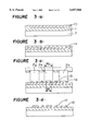
- FIGS. 2(a) through 2(d) are cross-sectional views of the mask for explaining manufacturing processes of the phase shift mask of attenuated type. These cross-sectional views are taken along a line V--V shown in FIG. 1.
- a numerical reference 1 designates a phase shift film of attenuated type
- a numerical reference 2 designates a pattern with concentrated apertures
- a numerical reference 7 designates a light transmittible substrate
- a numerical reference 8 designates a resist film for electron beam
- a numerical reference 13 designates a resist pattern for electron beam.
- the phase shift film of attenuated type 1 is formed to be a film thickness of 500 ⁇ through 2000 ⁇ .
- the phase shift film of attenuated type 1 is made of materials such as a Cr system or a MoSiON system having a transmittance of about 2 through 20% with respect to a wavelength of exposure and a phase shift of 180° with respect to an aperture of the light transmissible substrate.
- the resist for electron beam 8 is formed on the phase shift film of attenuated type 1. Further, as shown in FIG.
- a resist pattern for electron beam 13 is obtained such that data of a second pattern in an electron beam lithography system for forming a pattern including the patterns with an isolated aperture 3, 4 as shown in FIG. 1 and the pattern with concentrated apertures 2 as the first pattern is used to irradiate an electron beam on the resist for electron beam 8 and thereafter it is developed.
- the second data of pattern are obtained by converting the first data of pattern such that the second data represent a resist pattern in which the right side thereof is inverted to be the left with respect to the resist pattern obtained by the first data of pattern in the electron beam lithography system, which is used at a time of producing the phase shift mask of attenuated type having an optical proximity correction to be described below. As shown in FIG.
- phase shift mask of attenuated type 1 is etched using the resist pattern for electron beam 13 as a mask; and thereafter, the unnecessary resist is removed to complete a first phase shift mask of attenuated type including the pattern with concentrated apertures 2 and the patterns with an isolated aperture (not shown).
- FIGS. 3(a) through 3(d) and 4(e) through 4(h) are cross-sectional views of a mask for explaining steps of producing the phase shift mask of attenuated type having the optical proximity correction using the first phase shift mask of attenuated type. These cross-sectional views are taken along a line V--V in the first phase shift mask of attenuated type shown in FIG. 1.
- a numerical reference 10 designates a shading film
- a numerical reference 14 designates a negative resist film
- a numerical reference 15 designates an optical proximity correction of resist
- a numerical reference 16 designates a pattern of negative resist
- a numerical reference 17 designates an optical proximity correction
- a numerical reference 18 designates a pattern of shading film
- a numerical reference 19 designates a resist pattern for electron beam
- a numerical reference 20 designates a pattern of concentrated apertures.
- the other numerical references designate portions being the same as or similar to the references shown in FIG. 2.
- the phase shift film of attenuated type 1 and the shading film 10, both of which are optical members, are formed on the transmittible substrate 7 to be a film thickness of 500 ⁇ through 2000 ⁇ in a sequential manner, respectively.
- the phase shift film 1 is the phase shift film of attenuated type of a Cr system or a MoSiON system, which has a transmittance of about 2% through 20% with respect to a wavelength of exposure and a phase shift of 180° with respect to the apertures of the light transmittible substrate 1.
- the shading film 10 is made of materials such as Cr or MoSi.
- the negative resist film 14 is formed on the shading film 10 as the first resist film. Further, as shown in FIG.
- the wave length of the exposure light which is used for this exposure is preferably the same wavelength as that of exposure system which is used at the time of producing the semiconductor device, for example, an line beam (wavelength of 365 nm), a KrF laser beam (wavelength of 248 nm) and an ArF laser beam (wavelength of 193 nm).
- an line beam wavelength of 365 nm
- a KrF laser beam wavelength of 248 nm
- an ArF laser beam wavelength of 193 nm.
- a resist for electron beam 8 is formed on the whole surface of the pattern of shading film 18 including the optical proximity correction 17.
- an electron beam is irradiated on the resist film for electron beam 8 based on the first data of pattern in the electronic lithography system; and thereafter it is developed to thereby obtain the resist pattern for electron beam 19 as the second resist pattern.
- formed resist pattern for electron beam 19 is configurated such that only portions corresponding to the optical proximity correction 17 are covered and the pattern of shading film 18 is not covered.
- FIG. 5 is a plan view of thus completed phase shift mask of attenuated type having thus completed optical proximity correction.
- FIGS. 6(a) through 6(d) show cross-sectional views of the phase shift mask of attenuated type produced by the above method taken along a line VI--VI in FIG. 5, amplitude of an exposure light transmitted through the phase shift mask of attenuated type on the wafer surface, intensity of exposure light on the wafer surface and a cross-sectional view of the formed positive resist pattern.
- a numerical reference 311 designates a main peak light
- a numerical reference 312 designates a side lobe light
- a numerical reference 511 designates a positive resist pattern.
- the other numerical references designate portions the same as or similar to those shown in FIGS. 3(a) through 3(d) and FIGS. 4(e) through 4(h).
- An exposure light transmitted through the phase shift mask of attenuated type overlaps mutually in areas exposed by the light transmitted through the phase shift film of attenuated type, and a side lobe light 312 is generated as shown in FIG. 6(c).
- the optical proximity correction 17 made of a shading film is provided at a portion corresponding to the area, the intensity of the side lobe light 312 caused by the overlap is extremely weakened. Accordingly, a loss of the resist film is not caused by such side lobe light having weak intensity, and the resist pattern 511 having a resist pattern aperture 512 as designed is formed as shown in FIG. 6(d).
- FIGS. 7(a) through 7(c) steps of transferring a pattern image of the phase shift mask of attenuated type to the resist film on a light transmittible substrate, which is a workpiece to be processed, by an exposure system of 1:1.
- FIG. 7(a) is a plan view for showing a pattern image (for example, a letter of F) viewed from the side having a pattern of the phase shift mask of attenuated type;
- FIG. 7(b) is a cross-sectional view for showing a relation of arrangement of the exposure system when the resist pattern 21 is formed on the light transmittible substrate 7 using this phase shift mask of attenuated type; and FIG.
- FIGS. 7(a) through 7(c) are plan views for showing the pattern image viewed from the side having a pattern of the resist pattern 21 formed on the light transmittible substrate.
- a numerical reference 1 designates a phase shift film of attenuated type
- a numerical reference 7 designates the light transmittible substrate
- a numerical reference 21 designates the resist pattern.
- Embodiment 1 various transfer tests, various optical simulations and a large quantity of data for writing in an electron beam lithography system for optimizing optical proximity correction, which is different at each pattern size and at each pattern arrangement in the conventional technique, are no longer necessary and the cost for producing the photo mask is reduced and throughput is improved, because the optical proximity correction of the phase shift mask of attenuated type can be formed in a self-replicating manner by using the first phase shift mask of attenuated type produced based on the data of pattern of which left side is inverted right.
- Embodiment 1 an optical proximity correction made of a shading film is formed.
- Embodiment 2 an optical proximity correction composed of apertures is formed.
- FIGS. 8(a) through 8(d) and FIGS. 9(e) through 9(h) show cross-sectional views of a phase shift mask of attenuated type according to Embodiment 2, in which steps of a method of producing the phase shift mask are explained. These cross-sectional views are taken along a line V--V of the first phase shift mask of attenuated type shown in FIG. 1.
- the other references are portions the same as or similar to those shown in FIGS. 3(a) through 3(d) and FIGS. 4(e) through 4(h)As
- a phase shift film of attenuated type 1 is formed as an optical member on a light transmittible substrate 7.
- a positive resist film namely, the first resist film 22 is formed on this phase shift film of attenuated type 1.
- this positive resist film 22 is exposed using the first phase shift mask of attenuated type shown in FIG. 1 by an exposure system of 1:1, and thereafter it is developed to thereby form the first resist pattern 24 including the pattern of optical proximity correction 23 composed of apertures.
- the optical proximity correction is formed in a self-replicating manner in an area at which the optical proximity correction should be formed by a side lobe light generated by an overlap of an exposure light transmitted through a mask as described in Embodiment 1.
- a luminous exposure is adjusted such that the width W 2 of the aperture 25 in the first resist pattern 24 is narrower than the width W 0 of the aperture 2e in the first phase shift mask of attenuated type.
- the amount of reduction (W 0 -W 2 ) is preferably about 0.15 ⁇ m in consideration of accuracy in process of producing the mask, as in Embodiment 1.
- the wavelength of exposure light to be used therein is preferably the same as the wavelength of exposure light which is practically used at the time of producing the semiconductor device using the first phase shift mask of attenuated type 10, for example, an i-line beam (wavelength of 365 nm), a KrF laser beam (wavelength of 248 nm), an ArF laser beam (wavelength of 193 nm) or the like can be used.
- an i-line beam wavelength of 365 nm
- a KrF laser beam wavelength of 248 nm
- an ArF laser beam wavelength of 193 nm
- the phase shift mask of attenuated type 1 is etched using the first resist pattern 24 including the pattern of optical proximity correction 23 as a mask, and thereafter the unnecessary resist is removed, whereby the second pattern 26 including the optical proximity correction 27 made of the phase shift film of attenuated type is formed.
- a resist for electron beam 8 is formed on the second pattern 26.
- an electron beam is irradiated on the resist for electron beam 8 based on first data of pattern in an electronic lithography system; and thereafter it is developed to thereby obtain a resist pattern for electron beam 19.
- the resist pattern for electron beam 19 is formed on the second pattern 26 so as to cover the optical proximity correction 27 but not to cover the aperture 28 of the second pattern.
- the width W 2 of the aperture 25 in the first resist pattern 24 is formed to be narrower than the width W 0 of the aperture 2e in the first phase shift mask of attenuated type, which is originally planed to be formed, and accordingly the width of the aperture 28 in the second pattern formed by etching it as a mask is thus narrow.
- FIG. 9(g) a part of the second pattern is etched using the resist pattern for electron beam 19 as a mask; and thereafter the unnecessary resist is removed, whereby the phase shift mask of attenuated type having the pattern with concentrated apertures 50 and the optical proximity correction 27 as shown in FIG. 9(h) is completed.
- FIG. 10 is a plan view of this phase shift mask of attenuated type.
- FIGS. 11(a) through 11(d) respectively show a cross-sectional view of the phase shift mask of attenuated type produced in accordance with the above-mentioned method taken along a line VI--VI of FIG. 10, amplitude of exposure light transmitted through the phase shift mask of attenuated type on the wafer surface, intensity of the exposure light on the wafer surface and a cross-sectional view of the formed positive resist pattern.
- a numerical reference 321 designates a main peak light
- a numerical reference 322 designates a side lobe light
- a numerical reference 521 designates a positive resist pattern
- a numerical reference 522 designates an aperture in the resist.
- the other references designate portions the same as or similar to those shown in FIGS. 8(a) through 8(d) and FIGS. 9(e) through 9(h).
- the exposure light transmitted through the phase shift mask of attenuated type is overlapped in an area subjected to the exposure by the exposure light transmitted through the phase shift film of attenuated type as shown in FIG. 11(b), and thereby the side lobe light 322 is generated as shown in FIG. 11(c).
- the optical proximity correction 27 composed of apertures of phase shift film of attenuated type 1 is provided in a portion corresponding to the area, the intensity of side lobe light 322 caused by this overlap is extremely reduced. Accordingly, a loss of resist film is not caused by such side lobe light having weak intensity, whereby the resist pattern 521 having the aperture of resist 522 as designed can be formed as shown in FIG. 11(d).
- the optical proximity correction in the phase shift mask of attenuated type can be formed in a self-replicating manner using the phase shift mask of attenuated type produced based on only the data of pattern, which is obtained by inverting the optical proximity correction so as to be the left side right; and thereby it is not necessary to conduct various transfer tests and various optical simulations for optimizing the optical proximity correction, which is different at each pattern size and/or at each pattern arrangement, and to prepare a vast amount of data for writing in an electron beam lithography system not like the conventional technique.
- a mirror projection aligner as shown in FIG. 12 is used.
- a numerical reference 801 designates a light source
- a numerical reference 802 designates an optical system including a condenser lens and so on
- a numerical reference 803 designates a photo mask
- a numerical reference 804 designates a workpiece
- a numerical reference 805 designates a light reflector.
- the photo mask 803 and the workpiece 804 can be isolated completely and high resolution is obtainable in comparison with a contact aligner or a proximity aligner, whereby this mirror projection aligner is most preferable.
- FIGS. 13(a) through 13(d) and FIGS. 14(e) through 14(h) show cross-sectional views of, for example, an integrated circuit of MOS transistor for explaining a method of forming contact holes for connecting a semiconductor substrate with electrodes.
- a numerical reference 701 designates the semiconductor substrate; a numerical reference 702 designates a region of separating elements; a numerical reference 703 designates a region with impurity diffused; a numerical reference 704 designates an inter-layer insulating film; a numerical reference 705 designates a positive resist film; a numerical reference 706 designates an aperture of positive resist pattern; a numerical reference 707 designates a contact hole; a numerical reference 708 designates a metallic film; and a numerical reference 709 designates a positive resist film.
- the semiconductor substrate 701, the region of separating elements 702 and the region with impurity diffused 703, which are formed on the main surface of the semiconductor substrate 701, and the inter-layer insulating film 704, which is formed thereon, are provided.
- the semiconductor substrate 701 is, for example, a silicon substrate of P-type;
- the region of separating elements 702 has an ordinary localized oxidation of silicon (LOCOS) structure;
- the region with impurity diffused 703 is an n type diffusion layer by implanting arsenic (As) or the like.
- the inter-layer insulating film 704 is made of, for example, a phospho silicate glass (PSG) film or the like.
- PSG phospho silicate glass
- the positive resist film 705 is coated on this inter-layer insulating film 704 and the positive resist film 705 is exposed by, for example, an i-line stepper of i-line beam using the phase shift mask of attenuated type having the optical proximity correction provided with a predetermined pattern according to the present invention. Thereafter, the positive resist film 705 is developed, to thereby obtain a positive resist pattern 705a as shown in FIG. 13(c). Further, as shown in FIG. 13(d), the inter-layer insulating film 704 is subjected to an etching by dry etching using the positive resist pattern 705a as a mask and also using, for example, etching gas of freon system, to thereby form the contact hole 707. Thereafter, the unnecessary resist is removed.
- a metallic film 708 made of aluminum or the like is formed on the inter-layer insulating film 704, in which the contact hole 707 is formed. Further, as shown in FIG. 14(f) of FIG. 14, the positive resist film 709 is coated on this metallic film 708. As shown in FIG. 14(g), the positive resist film 709 is exposed using a photo mask provided with a predetermined pattern, and thereafter it is developed to thereby obtain a resist pattern 709a. At last, as shown in FIG. 14(h), the metallic film 708 is etched using the resist pattern 709a as a mask, and thereafter the unnecessary resist is removed, to thereby obtain a predetermined electrode 708a which is electrically connected with the impurity region 703 through the contact hole 707.
- the present invention provides and effects of drastically reducing the production time and the manufacturing cost because it is not necessary to make data for writing the optical proximity correction at the time of forming by the electron beam lithography system, to conduct transfer tests and/or optical simulations both for optimizing, and to prepare very large amount of data for writing in the electron beam lithography system, as long as the optical proximity correction is formed in the self-replicating manner using the phase shift mask of attenuated type.
Abstract
Description
Claims (8)
Applications Claiming Priority (2)
| Application Number | Priority Date | Filing Date | Title |
|---|---|---|---|
| JP10802598A JPH11305415A (en) | 1998-04-17 | 1998-04-17 | Production of photomask |
| JP10-108025 | 1998-04-17 |
Publications (1)
| Publication Number | Publication Date |
|---|---|
| US6057066A true US6057066A (en) | 2000-05-02 |
Family
ID=14474070
Family Applications (1)
| Application Number | Title | Priority Date | Filing Date |
|---|---|---|---|
| US09/154,071 Expired - Lifetime US6057066A (en) | 1998-04-17 | 1998-09-16 | Method of producing photo mask |
Country Status (2)
| Country | Link |
|---|---|
| US (1) | US6057066A (en) |
| JP (1) | JPH11305415A (en) |
Cited By (8)
| Publication number | Priority date | Publication date | Assignee | Title |
|---|---|---|---|---|
| US6194103B1 (en) * | 1999-07-08 | 2001-02-27 | Taiwan Semiconductor Manufacturing Company | E-beam double exposure method for manufacturing ASPM mask with chrome border |
| US6214497B1 (en) * | 1999-06-29 | 2001-04-10 | Micron Technology, Inc. | Method to eliminate side lobe printing of attenuated phase shift masks |
| US20030196178A1 (en) * | 2002-04-11 | 2003-10-16 | International Business Machines Corporation | Trough adjusted optical proximity correction for vias |
| US6653231B2 (en) * | 2001-03-28 | 2003-11-25 | Advanced Micro Devices, Inc. | Process for reducing the critical dimensions of integrated circuit device features |
| US6828259B2 (en) | 2001-03-28 | 2004-12-07 | Advanced Micro Devices, Inc. | Enhanced transistor gate using E-beam radiation |
| US20070254218A1 (en) * | 2006-04-28 | 2007-11-01 | Promos Technologies Inc. | Phase shifting mask capable of reducing the optical proximity effect and method for preparing semiconductor devices using the same |
| US7354682B1 (en) * | 2004-07-09 | 2008-04-08 | Advanced Micro Devices, Inc. | Chromeless mask for contact holes |
| US8539392B2 (en) | 2011-02-24 | 2013-09-17 | National Taiwan University | Method for compensating proximity effects of particle beam lithography processes |
Families Citing this family (2)
| Publication number | Priority date | Publication date | Assignee | Title |
|---|---|---|---|---|
| JP2002244271A (en) * | 2001-02-15 | 2002-08-30 | Oki Electric Ind Co Ltd | Mask for manufacturing semiconductor and semiconductor manufacturing method |
| JP4539061B2 (en) * | 2003-09-08 | 2010-09-08 | 凸版印刷株式会社 | Phase shift mask manufacturing method, phase shift mask, and semiconductor device manufacturing method |
Citations (3)
| Publication number | Priority date | Publication date | Assignee | Title |
|---|---|---|---|---|
| JPH0764273A (en) * | 1993-08-27 | 1995-03-10 | Sony Corp | Phase shift mask |
| JPH08279452A (en) * | 1995-03-16 | 1996-10-22 | Lg Semicon Co Ltd | Preparation of phase shift mask |
| US5853923A (en) * | 1997-10-23 | 1998-12-29 | Taiwan Semiconductor Manufacturing Company, Ltd. | Double layer method for fabricating a rim type attenuating phase shifting mask |
-
1998
- 1998-04-17 JP JP10802598A patent/JPH11305415A/en active Pending
- 1998-09-16 US US09/154,071 patent/US6057066A/en not_active Expired - Lifetime
Patent Citations (3)
| Publication number | Priority date | Publication date | Assignee | Title |
|---|---|---|---|---|
| JPH0764273A (en) * | 1993-08-27 | 1995-03-10 | Sony Corp | Phase shift mask |
| JPH08279452A (en) * | 1995-03-16 | 1996-10-22 | Lg Semicon Co Ltd | Preparation of phase shift mask |
| US5853923A (en) * | 1997-10-23 | 1998-12-29 | Taiwan Semiconductor Manufacturing Company, Ltd. | Double layer method for fabricating a rim type attenuating phase shifting mask |
Cited By (9)
| Publication number | Priority date | Publication date | Assignee | Title |
|---|---|---|---|---|
| US6214497B1 (en) * | 1999-06-29 | 2001-04-10 | Micron Technology, Inc. | Method to eliminate side lobe printing of attenuated phase shift masks |
| US6194103B1 (en) * | 1999-07-08 | 2001-02-27 | Taiwan Semiconductor Manufacturing Company | E-beam double exposure method for manufacturing ASPM mask with chrome border |
| US6653231B2 (en) * | 2001-03-28 | 2003-11-25 | Advanced Micro Devices, Inc. | Process for reducing the critical dimensions of integrated circuit device features |
| US6828259B2 (en) | 2001-03-28 | 2004-12-07 | Advanced Micro Devices, Inc. | Enhanced transistor gate using E-beam radiation |
| US20030196178A1 (en) * | 2002-04-11 | 2003-10-16 | International Business Machines Corporation | Trough adjusted optical proximity correction for vias |
| US6760901B2 (en) | 2002-04-11 | 2004-07-06 | International Business Machines Corporation | Trough adjusted optical proximity correction for vias |
| US7354682B1 (en) * | 2004-07-09 | 2008-04-08 | Advanced Micro Devices, Inc. | Chromeless mask for contact holes |
| US20070254218A1 (en) * | 2006-04-28 | 2007-11-01 | Promos Technologies Inc. | Phase shifting mask capable of reducing the optical proximity effect and method for preparing semiconductor devices using the same |
| US8539392B2 (en) | 2011-02-24 | 2013-09-17 | National Taiwan University | Method for compensating proximity effects of particle beam lithography processes |
Also Published As
| Publication number | Publication date |
|---|---|
| JPH11305415A (en) | 1999-11-05 |
Similar Documents
| Publication | Publication Date | Title |
|---|---|---|
| KR100187866B1 (en) | High resolution phase edge lithography without the need for a trim mask | |
| KR100283836B1 (en) | Method of manufacturing semiconductor device and exposure mask | |
| JP4646367B2 (en) | Semiconductor device manufacturing method and semiconductor device | |
| JP2000206667A (en) | Photomask and exposure method using photomask | |
| JP2007086368A (en) | Photomask, its manufacturing method, and manufacturing method of semiconductor device | |
| US6828080B2 (en) | Pattern forming method and method of fabricating device | |
| US6057066A (en) | Method of producing photo mask | |
| JP3912949B2 (en) | Photomask forming method and semiconductor device manufacturing method | |
| US6905899B2 (en) | Methods for forming a photoresist pattern using an anti-optical proximity effect | |
| JP2003255510A (en) | Method for manufacturing electronic device | |
| US5837426A (en) | Photolithographic process for mask programming of read-only memory devices | |
| US5589303A (en) | Self-aligned opaque regions for attenuating phase-shifting masks | |
| US6376130B1 (en) | Chromeless alternating reticle for producing semiconductor device features | |
| US7141338B2 (en) | Sub-resolution sized assist features | |
| JP3164039B2 (en) | Photomask and method of manufacturing the same | |
| US6187486B1 (en) | Method of multi-exposure for improving photolithography resolution | |
| US20070148558A1 (en) | Double metal collimated photo masks, diffraction gratings, optics system, and method related thereto | |
| JP2000019710A (en) | Manufacture of semiconductor integrated circuit device | |
| US6563127B2 (en) | Optical proximity correction with rectangular contact | |
| US6670109B2 (en) | Photolithographic methods of using a single reticle to form overlapping patterns | |
| US20070015088A1 (en) | Method for lithographically printing tightly nested and isolated hole features using double exposure | |
| KR20030056499A (en) | Mask for Forming Minute Pattern | |
| US7012763B2 (en) | Aperture plate for lithography systems | |
| JPH0961990A (en) | Phase shift mask and its production as well as exposure method using the same | |
| US6316340B1 (en) | Photolithographic process for preventing corner rounding |
Legal Events
| Date | Code | Title | Description |
|---|---|---|---|
| AS | Assignment |
Owner name: MITSUBISHI DENKI KABUSHIKI KAISHA, JAPAN Free format text: ASSIGNMENT OF ASSIGNORS INTEREST;ASSIGNOR:HANAWA, TETSURO;REEL/FRAME:009474/0886 Effective date: 19980806 |
|
| FEPP | Fee payment procedure |
Free format text: PAYOR NUMBER ASSIGNED (ORIGINAL EVENT CODE: ASPN); ENTITY STATUS OF PATENT OWNER: LARGE ENTITY |
|
| STCF | Information on status: patent grant |
Free format text: PATENTED CASE |
|
| FPAY | Fee payment |
Year of fee payment: 4 |
|
| FPAY | Fee payment |
Year of fee payment: 8 |
|
| AS | Assignment |
Owner name: RENESAS ELECTRONICS CORPORATION, JAPAN Free format text: ASSIGNMENT OF ASSIGNORS INTEREST;ASSIGNOR:MITSUBISHI DENKI KABUSHIKI KAISHA;REEL/FRAME:025980/0219 Effective date: 20110307 |
|
| FPAY | Fee payment |
Year of fee payment: 12 |
|
| AS | Assignment |
Owner name: RENESAS ELECTRONICS CORPORATION, JAPAN Free format text: CHANGE OF ADDRESS;ASSIGNOR:RENESAS ELECTRONICS CORPORATION;REEL/FRAME:044928/0001 Effective date: 20150806 |