US5970357A - Method and structure for manufacturing high-resistance polysilicon loads in a semiconductor process - Google Patents
Method and structure for manufacturing high-resistance polysilicon loads in a semiconductor process Download PDFInfo
- Publication number
- US5970357A US5970357A US09/081,299 US8129998A US5970357A US 5970357 A US5970357 A US 5970357A US 8129998 A US8129998 A US 8129998A US 5970357 A US5970357 A US 5970357A
- Authority
- US
- United States
- Prior art keywords
- polysilicon
- loads
- layer
- dielectric layer
- resistance
- Prior art date
- Legal status (The legal status is an assumption and is not a legal conclusion. Google has not performed a legal analysis and makes no representation as to the accuracy of the status listed.)
- Expired - Fee Related
Links
Images


Classifications
-
- H—ELECTRICITY
- H10—SEMICONDUCTOR DEVICES; ELECTRIC SOLID-STATE DEVICES NOT OTHERWISE PROVIDED FOR
- H10B—ELECTRONIC MEMORY DEVICES
- H10B10/00—Static random access memory [SRAM] devices
-
- H—ELECTRICITY
- H10—SEMICONDUCTOR DEVICES; ELECTRIC SOLID-STATE DEVICES NOT OTHERWISE PROVIDED FOR
- H10B—ELECTRONIC MEMORY DEVICES
- H10B10/00—Static random access memory [SRAM] devices
- H10B10/15—Static random access memory [SRAM] devices comprising a resistor load element
Definitions
- the invention relates to a semiconductor process, and in particular to a method and a structure for manufacturing high-resistance polysilicon loads in the semiconductor process.
- polysilicon layers are commonly used as loads in 4T SRAM memory cells.
- a polysilicon layer is first deposited. Then, a high-energy ion implantation is performed to adjust the resistance thereof. After that, the polysilicon layer is patterned to form a plurality of polysilicon loads by photolithography and etching techniques. Next, parts of the polysilicon loads are ion implanted with a high-concentration dopant, thereby forming the required connectors.
- FIG. 1 a structure of polysilicon loads manufactured by the prior art is shown. In FIG.
- FIG. 1 is a top view of FIG. 1.
- FIG. 1 is a cross-sectional view of FIG. 2 along line I--I.
- the resistance of the polysilicon loads depends on the amount of the first implanted dopant, the thicknesses, widths and lengths of the polysilicon loads etc. In order to obtain sufficient high-resistance loads, a traditional method is used to reduce the thicknesses, increase the lengths or decrease the widths of polysilicon loads.
- the objective of the invention is to provide a method which greatly increases the lengths of polysilicon loads without increasing the sizes of memory cells, thereby resolving the above-mentioned problem.
- the method for manufacturing high-resistance polysilicon loads in the semiconductor process according to the invention comprises the following steps: First, a first dielectric layer is formed on the substrate and the conductive layers. A trench is formed in the first dielectric layer. Consequently, a second dielectric layer protruding over the surface of the first dielectric layer, is formed in the trench. Spacers are formed on both sides of the second dielectric layer over the surface of the first dielectric layer. Thereafter, the second dielectric layer is removed.
- a plurality of contact windows are formed in the first dielectric layer just on the conductive layer.
- a polysilicon layer is formed on the first dielectric layer, the contact windows, the spacers and the trench.
- a first ion implantation is performed on the polysilicon layer.
- the polysilicon layer is patterned to form a plurality of polysilicon loads perpendicular to the trench and the spacers, then a second ion implantation is performed on parts of the polysilicon loads just on the contact windows and another intended parts of the polysilicon loads.
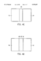
- FIG. 1 is a cross-sectional view showing a structure of a polysilicon load manufactured by the prior art
- FIG. 2 is a top view of FIG. 2;
- FIGS. 3A ⁇ 3H are cross-sectional views showing a method for manufacturing high-resistance polysilicon loads according to the invention.
- FIGS. 4A ⁇ 4H are top views of FIGS. 3A ⁇ 3H, respectively.
- This method suitable for a substrate 10 in which a plurality of conductive layers (just one of them shown) 11, such as first polysilicon layers, are already formed, comprises the following steps:
- a first dielectric layer 12 such as an undoped TEOS layer, is formed on the substrate 10 and the first polysilicon layers 11 by using chemical vapor deposition.
- a first photoresist 13 is formed on the undoped TEOS layer 12 by photolithography. Then a trench 14 with a depth of d1 is formed in the undoped TEOS layer 12 by plasma etching.
- LPD liquid phase deposition
- the first photoresist 13 is first removed by wet etching.
- a dielectric layer (not shown), such as an undoped TEOS layer, is formed on the undoped TEOS layer 12 and the doped oxide layer 15.
- this dielectric layer is etched back by an isotropic etching, thereby forming spacers 16, such as undoped TEOS spacers, on both sides of the doped TEOS layer 15 over the surface of the undoped TEOS layer 12.
- the doped TEOS layer 15 is removed by a selective etching with a vapor of HF.
- a second photoresist 17 is first formed on the undoped TEOS layer 12, the undoped TEOS spacers 16 and the trench 14 by photolithography. Consequently, contact windows 18 are formed in the undoped TEOS layer 12 just on the first polysilicon layers by plasma etching.
- the second photoresist 17 is previously removed by wet etching. Then, a second polysilicon layer 19 is formed on the undoped TEOS layer 12, the contact windows 18, the spacers 16 and the trench 14 by chemical vapor deposition. Thereafter, a first ion implantation is performed on the second polysilicon layer 19, thereby adjusting the resistance thereof.
- the second polysilicon layer 19 is patterned to form a plurality of polysilicon loads 19' perpendicular to the trench 14 and the spacers 16 (just one of them shown), then a second ion implantation is performed on parts of the polysilicon loads 19' just over the contact windows 18 and other intended parts of the polysilicon loads to form connectors 20.
- FIGS. 4A ⁇ 4H are top views corresponding to FIG. 3A ⁇ 3H with the same reference numerals.
- the trench 14 formed in the undoped TEOS layer 12 is perpendicular to the polysilicon loads 19'. Basically, the depth d1 of the trench 14 less than the thickness of the updoped TEOS layer 12 is taken as a rule.
- the doped oxide layer 15 is formed only in the trench 14 by liquid phase deposition before removing the first photolithography 13. Part of the doped oxide layer 15 protruding over the surface of the undoped TEOS layer 12 has a height of d2.
- the undoped TEOS spacers 16 are formed on both sides of the doped oxide layer 15 by etching back the undoped TEOS layer (not shown). After that, the doped oxide layer 15 is removed by selective etching, exposing the trench 14 again. However, the spacers 16 still remain on the surface of the undoped TEOS layer 12,
- each polysilicon load 19' Since the trench 14 and spacer 16 are perpendicular to the polysilicon loads 19', the effective lengths of the polysilicon loads are increased.
- the increased length of each polysilicon load 19' is twice the d1 value plus 4 times the d2 value. For example, if the d1 value is 1,000 ⁇ and the d2 value is 1,000 ⁇ , the length of each polysilicon load is increased about 0.6 ⁇ m; if the d1 value is 2,500 ⁇ and the d2 value is 1,000 ⁇ , the length of each polysilicon load is increased about 1.2 ⁇ m. Therefore, the effective length of each polysilicon load can be easily adjusted by controlling the d1 and d2 values so as to meet the requirements of memory cells. In other words, since the lengths of polysilicon loads are increased, the influence of out-diffusion is reduced, and limitation to the miniaturization of memories is mostly eliminated when manufacturing high-resistance polysilicon loads.
Landscapes
- Semiconductor Memories (AREA)
Abstract
High-resistance polysilicon layers applied in 4T SRAM memory cells serving as loads, are manufactured by a simple method according to the invention. In the small-scale 4T SRAM memory cell process, it is not possible to fabricate traditional polysilicon loads manufactured by the prior art with a desired high degree of resistance. As a result, the miniaturization of 4T SRAM memory cells has been limited. However, in the method according to the invention, the lengths of polysilicon loads are greatly increased without increasing the sizes of corresponding memory cells, thereby efficiently increasing the resistance of the polysilicon loads. Therefore, this method according to invention can completely eliminate any limitation to the small-scale 4T SRAM memory cell process caused by the manufacture of the polysilicon loads as described above.
Description
1. Field of the Invention
The invention relates to a semiconductor process, and in particular to a method and a structure for manufacturing high-resistance polysilicon loads in the semiconductor process.
2. Description of the Related Art
As is well known, high-resistance polysilicon layers are commonly used as loads in 4T SRAM memory cells. Traditionally, to manufacture polysilicon loads, a polysilicon layer is first deposited. Then, a high-energy ion implantation is performed to adjust the resistance thereof. After that, the polysilicon layer is patterned to form a plurality of polysilicon loads by photolithography and etching techniques. Next, parts of the polysilicon loads are ion implanted with a high-concentration dopant, thereby forming the required connectors. Referring to FIG. 1, a structure of polysilicon loads manufactured by the prior art is shown. In FIG. 1, reference numerals 10, 11, 12, 19' and 20 represent a substrate, polysilicon layers, a TEOS layer, polysilicon loads and connectors, respectively. The FIG. 2 is a top view of FIG. 1. In other words, the FIG. 1 is a cross-sectional view of FIG. 2 along line I--I. Clearly, the resistance of the polysilicon loads depends on the amount of the first implanted dopant, the thicknesses, widths and lengths of the polysilicon loads etc. In order to obtain sufficient high-resistance loads, a traditional method is used to reduce the thicknesses, increase the lengths or decrease the widths of polysilicon loads. However, with miniaturization of memory cells, this traditional method can no longer produce polysilicon loads of sufficient high-resistance. The reason is that out-diffusion caused by dopant inside the connectors greatly shortens the effective lengths of such polysilicon loads. In the past, increasing the lengths of polysilicon loads has been limited by the miniaturization of memory cells. Reducing the widths of polysilicon loads has been limited by processing capabilities. Therefore, the drawbacks of the traditional method of manufacturing polysilicon loads has been one of the factors to affect the miniaturization of memories.
In view of the above, the objective of the invention is to provide a method which greatly increases the lengths of polysilicon loads without increasing the sizes of memory cells, thereby resolving the above-mentioned problem. The method for manufacturing high-resistance polysilicon loads in the semiconductor process according to the invention, suitable for a substrate in which a plurality of conductive layers are already formed, comprises the following steps: First, a first dielectric layer is formed on the substrate and the conductive layers. A trench is formed in the first dielectric layer. Consequently, a second dielectric layer protruding over the surface of the first dielectric layer, is formed in the trench. Spacers are formed on both sides of the second dielectric layer over the surface of the first dielectric layer. Thereafter, the second dielectric layer is removed. A plurality of contact windows are formed in the first dielectric layer just on the conductive layer. Then, a polysilicon layer is formed on the first dielectric layer, the contact windows, the spacers and the trench. A first ion implantation is performed on the polysilicon layer. Finally, the polysilicon layer is patterned to form a plurality of polysilicon loads perpendicular to the trench and the spacers, then a second ion implantation is performed on parts of the polysilicon loads just on the contact windows and another intended parts of the polysilicon loads.
The present invention will become more fully understood from the detailed description given hereinbelow and the accompanying drawings which are given by way of illustration only, and thus are not limitative of the present invention, and wherein:
FIG. 1 is a cross-sectional view showing a structure of a polysilicon load manufactured by the prior art;
FIG. 2 is a top view of FIG. 2;
FIGS. 3A˜3H are cross-sectional views showing a method for manufacturing high-resistance polysilicon loads according to the invention; and
FIGS. 4A˜4H are top views of FIGS. 3A˜3H, respectively.
Referring to FIGS. 3A˜3H, a method for manufacturing high-resistance polysilicon loads according to the invention is shown. This method, suitable for a substrate 10 in which a plurality of conductive layers (just one of them shown) 11, such as first polysilicon layers, are already formed, comprises the following steps:
Step 1
As shown in FIG. 3A, a first dielectric layer 12, such as an undoped TEOS layer, is formed on the substrate 10 and the first polysilicon layers 11 by using chemical vapor deposition.
Step 2
As shown in FIG. 3B, a first photoresist 13 is formed on the undoped TEOS layer 12 by photolithography. Then a trench 14 with a depth of d1 is formed in the undoped TEOS layer 12 by plasma etching.
Step 3
As shown in FIG. 3C, a second dielectric layer 15, such as a doped oxide layer, the height of which protrudes over the surface of the undoped TEOS layer 12 by a height of d2, is formed in the trench 14 by liquid phase deposition (LPD).
Step 4
As shown in FIG. 3D, the first photoresist 13 is first removed by wet etching. After that, a dielectric layer (not shown), such as an undoped TEOS layer, is formed on the undoped TEOS layer 12 and the doped oxide layer 15. Then, this dielectric layer is etched back by an isotropic etching, thereby forming spacers 16, such as undoped TEOS spacers, on both sides of the doped TEOS layer 15 over the surface of the undoped TEOS layer 12.
Step 5
As shown in FIG. 3E, the doped TEOS layer 15 is removed by a selective etching with a vapor of HF.
Step 6
As shown in FIG. 3F, a second photoresist 17 is first formed on the undoped TEOS layer 12, the undoped TEOS spacers 16 and the trench 14 by photolithography. Consequently, contact windows 18 are formed in the undoped TEOS layer 12 just on the first polysilicon layers by plasma etching.
Step 7
As shown in FIG. 3G, the second photoresist 17 is previously removed by wet etching. Then, a second polysilicon layer 19 is formed on the undoped TEOS layer 12, the contact windows 18, the spacers 16 and the trench 14 by chemical vapor deposition. Thereafter, a first ion implantation is performed on the second polysilicon layer 19, thereby adjusting the resistance thereof.
Step 8
As shown in FIG. 3H, the second polysilicon layer 19 is patterned to form a plurality of polysilicon loads 19' perpendicular to the trench 14 and the spacers 16 (just one of them shown), then a second ion implantation is performed on parts of the polysilicon loads 19' just over the contact windows 18 and other intended parts of the polysilicon loads to form connectors 20.
Furthermore, FIGS. 4A˜4H are top views corresponding to FIG. 3A˜3H with the same reference numerals.
In addition, the characteristics of the invention will be described hereinafter.
(a) The trench 14 formed in the undoped TEOS layer 12 is perpendicular to the polysilicon loads 19'. Basically, the depth d1 of the trench 14 less than the thickness of the updoped TEOS layer 12 is taken as a rule.
(b) The doped oxide layer 15 is formed only in the trench 14 by liquid phase deposition before removing the first photolithography 13. Part of the doped oxide layer 15 protruding over the surface of the undoped TEOS layer 12 has a height of d2.
(c) The undoped TEOS spacers 16 are formed on both sides of the doped oxide layer 15 by etching back the undoped TEOS layer (not shown). After that, the doped oxide layer 15 is removed by selective etching, exposing the trench 14 again. However, the spacers 16 still remain on the surface of the undoped TEOS layer 12,
(d) Since the trench 14 and spacer 16 are perpendicular to the polysilicon loads 19', the effective lengths of the polysilicon loads are increased. The increased length of each polysilicon load 19' is twice the d1 value plus 4 times the d2 value. For example, if the d1 value is 1,000Å and the d2 value is 1,000Å, the length of each polysilicon load is increased about 0.6 μm; if the d1 value is 2,500Å and the d2 value is 1,000Å, the length of each polysilicon load is increased about 1.2 μm. Therefore, the effective length of each polysilicon load can be easily adjusted by controlling the d1 and d2 values so as to meet the requirements of memory cells. In other words, since the lengths of polysilicon loads are increased, the influence of out-diffusion is reduced, and limitation to the miniaturization of memories is mostly eliminated when manufacturing high-resistance polysilicon loads.
Although the invention has been disclosed in terms of a preferred embodiment, the disclosure is not intended to limit the invention. Those knowledgeable in the art can make modifications within the scope and spirit of the invention which is determined by the claims below.
Claims (8)
1. A method for manufacturing high-resistance polysilicon loads in a semiconductor process, suitable for a substrate in which a plurality of conductive layers are already formed, comprising:
forming a first dielectric layer on said substrate and said conductive layers;
forming a trench in said first dielectric layer and said substrate;
forming a second dielectric layer protruding over the surface of said first dielectric layer, in said trench;
forming spacers on both sides of said second dielectric layer over the surface of said first dielectric layer;
removing said second dielectric layer;
forming a plurality of contact windows in said first dielectric layer and said substrate just over said conductive layers;
forming a polysilicon layer on said first dielectric layer, said contact windows, said spacers and said trench; and
patterning said polysilicon layer to form polysilicon loads on sidewalls of said trench and said spacers.
2. A method for manufacturing high-resistance polysilicon loads in a semiconductor process as claimed in claim 1, further comprising performing a first ion implantation on said polysilicon layer before patterning said polysilicon layer.
3. A method for manufacturing high-resistance polysilicon loads in a semiconductor process as claimed in claim 1, further comprising performing a second ion implantation on parts of said polysilicon loads just over said contact windows and other intended parts of said polysilicon loads after patterning said polysilicon layer.
4. A method for manufacturing high-resistance polysilicon loads in a semiconductor process as claimed in claim 1, wherein said conductive layers are polysilicon layers.
5. A method for manufacturing high-resistance polysilicon loads in a semiconductor process as claimed in claim 1, wherein said first dielectric layer is an undoped TEOS layer.
6. A method for manufacturing high-resistance polysilicon loads in a semiconductor process as claimed in claim 1, wherein said second dielectric layer is a doped oxide layer.
7. A method for manufacturing high-resistance polysilicon loads in a semiconductor process as claimed in claim 6, wherein said doped oxide layer is removed by selective etching with a vapor of HF.
8. A method for manufacturing high-resistance polysilicon loads in a semiconductor process as claimed in claim 1, wherein said spacers are undoped TEOS layers.
Applications Claiming Priority (2)
| Application Number | Priority Date | Filing Date | Title |
|---|---|---|---|
| TW87106800 | 1998-05-02 | ||
| TW87106800 | 1998-05-02 |
Publications (1)
| Publication Number | Publication Date |
|---|---|
| US5970357A true US5970357A (en) | 1999-10-19 |
Family
ID=21630023
Family Applications (1)
| Application Number | Title | Priority Date | Filing Date |
|---|---|---|---|
| US09/081,299 Expired - Fee Related US5970357A (en) | 1998-05-02 | 1998-05-20 | Method and structure for manufacturing high-resistance polysilicon loads in a semiconductor process |
Country Status (1)
| Country | Link |
|---|---|
| US (1) | US5970357A (en) |
Cited By (1)
| Publication number | Priority date | Publication date | Assignee | Title |
|---|---|---|---|---|
| US6069063A (en) * | 1999-04-01 | 2000-05-30 | Taiwan Semiconductor Manufacturing Company | Method to form polysilicon resistors shielded from hydrogen intrusion |
Citations (5)
| Publication number | Priority date | Publication date | Assignee | Title |
|---|---|---|---|---|
| US5352923A (en) * | 1993-03-25 | 1994-10-04 | Northern Telecom Limited | Trench resistors for integrated circuits |
| US5602408A (en) * | 1994-04-25 | 1997-02-11 | Seiko Instruments Inc. | Semiconductor device having polycrystalline silicon load devices |
| US5757053A (en) * | 1994-06-27 | 1998-05-26 | Taiwan Semiconductor Manufacturing Company Ltd. | Effective load length increase by topography |
| US5861331A (en) * | 1998-04-20 | 1999-01-19 | United Microelectronics Corp. | Method for fabricating capacitors of a dynamic random access memory |
| US5885862A (en) * | 1996-06-27 | 1999-03-23 | Winbond Electronics Corp. | Poly-load resistor for SRAM cell |
-
1998
- 1998-05-20 US US09/081,299 patent/US5970357A/en not_active Expired - Fee Related
Patent Citations (5)
| Publication number | Priority date | Publication date | Assignee | Title |
|---|---|---|---|---|
| US5352923A (en) * | 1993-03-25 | 1994-10-04 | Northern Telecom Limited | Trench resistors for integrated circuits |
| US5602408A (en) * | 1994-04-25 | 1997-02-11 | Seiko Instruments Inc. | Semiconductor device having polycrystalline silicon load devices |
| US5757053A (en) * | 1994-06-27 | 1998-05-26 | Taiwan Semiconductor Manufacturing Company Ltd. | Effective load length increase by topography |
| US5885862A (en) * | 1996-06-27 | 1999-03-23 | Winbond Electronics Corp. | Poly-load resistor for SRAM cell |
| US5861331A (en) * | 1998-04-20 | 1999-01-19 | United Microelectronics Corp. | Method for fabricating capacitors of a dynamic random access memory |
Cited By (1)
| Publication number | Priority date | Publication date | Assignee | Title |
|---|---|---|---|---|
| US6069063A (en) * | 1999-04-01 | 2000-05-30 | Taiwan Semiconductor Manufacturing Company | Method to form polysilicon resistors shielded from hydrogen intrusion |
Similar Documents
| Publication | Publication Date | Title |
|---|---|---|
| EP0732738B1 (en) | DRAM capacitor electrode process | |
| EP1087443A2 (en) | Self-aligned non-volatile random access memory cell and process to make the same | |
| EP1087442A2 (en) | Floating gate memory array and self-aligned method of fabrication therefor | |
| US7332397B2 (en) | Method for fabricating semiconductor device | |
| US6153904A (en) | Fabrication method for increasing the coupling efficiency of ETOX flash memory devices | |
| JPH1050947A (en) | Manufacture of capacitor of semiconductor memory element | |
| KR100235122B1 (en) | Process of fabricating dynamic random access memory cell having inter-level insulating structure without silicon nitride layer between access transistor and storage node | |
| KR0138308B1 (en) | Method of fabricating interlayer connection in semiconductor device | |
| US5104821A (en) | Method for fabricating stacked capacitors in a DRAM cell | |
| US5907774A (en) | Corrugated post capacitor and method of fabricating using selective silicon deposition | |
| CN211789012U (en) | Semiconductor memory device with a plurality of memory cells | |
| KR970000977B1 (en) | Capacitor producing method of semiconductor device | |
| US5488008A (en) | Method of fabricating a stacked capacitor memory cell in a semiconductor memory device | |
| KR20040023716A (en) | Method of manufacturing a semiconductor device with a non-volatile memory comprising a memory cell with an access gate and with a control gate and a charge storage region | |
| US5970357A (en) | Method and structure for manufacturing high-resistance polysilicon loads in a semiconductor process | |
| JPH08316340A (en) | Fabrication of semiconductor device | |
| CN111524888B (en) | Semiconductor memory device and method of manufacturing the same | |
| US6020235A (en) | Channel-type stack capacitor for DRAM cell | |
| US6287982B1 (en) | Method of removing a portion of a silicon oxide form over stacked polysilicon and silicide layers by using hydrofluorine (HF) solution | |
| US6232222B1 (en) | Method of eliminating a critical mask using a blockout mask and a resulting semiconductor structure | |
| US6093602A (en) | Method to form polycide local interconnects between narrowly-spaced features while eliminating stringers | |
| US6271072B1 (en) | Method of manufacturing a storage node having five polysilicon bars | |
| KR100250749B1 (en) | Method for fabricating a storage node of capacitor | |
| KR950005478B1 (en) | Making method of polycied gate | |
| KR960015526B1 (en) | Semiconductor device and the manufacturing method |
Legal Events
| Date | Code | Title | Description |
|---|---|---|---|
| AS | Assignment |
Owner name: WINBOND ELECTRONICS CORP., TAIWAN Free format text: ASSIGNMENT OF ASSIGNORS INTEREST;ASSIGNOR:CHANG, MING-LUN;REEL/FRAME:009186/0046 Effective date: 19980420 |
|
| FPAY | Fee payment |
Year of fee payment: 4 |
|
| FPAY | Fee payment |
Year of fee payment: 8 |
|
| REMI | Maintenance fee reminder mailed | ||
| LAPS | Lapse for failure to pay maintenance fees | ||
| STCH | Information on status: patent discontinuation |
Free format text: PATENT EXPIRED DUE TO NONPAYMENT OF MAINTENANCE FEES UNDER 37 CFR 1.362 |
|
| FP | Lapsed due to failure to pay maintenance fee |
Effective date: 20111019 |