US5926938A - Method for working an electroformed magnetic metal sheet - Google Patents
Method for working an electroformed magnetic metal sheet Download PDFInfo
- Publication number
- US5926938A US5926938A US08/858,986 US85898697A US5926938A US 5926938 A US5926938 A US 5926938A US 85898697 A US85898697 A US 85898697A US 5926938 A US5926938 A US 5926938A
- Authority
- US
- United States
- Prior art keywords
- metal sheet
- plane
- back side
- magnet
- clamping
- Prior art date
- Legal status (The legal status is an assumption and is not a legal conclusion. Google has not performed a legal analysis and makes no representation as to the accuracy of the status listed.)
- Expired - Fee Related
Links
- 238000000034 method Methods 0.000 title claims abstract description 32
- 239000002184 metal Substances 0.000 title claims abstract description 20
- 229910052751 metal Inorganic materials 0.000 title claims abstract description 20
- 238000000227 grinding Methods 0.000 claims description 9
- 238000007493 shaping process Methods 0.000 claims description 8
- 239000004922 lacquer Substances 0.000 claims description 5
- 238000005266 casting Methods 0.000 claims description 4
- 238000003801 milling Methods 0.000 claims description 3
- 229920003023 plastic Polymers 0.000 claims description 3
- 238000006243 chemical reaction Methods 0.000 claims description 2
- 238000001746 injection moulding Methods 0.000 claims description 2
- 238000009713 electroplating Methods 0.000 abstract description 7
- PXHVJJICTQNCMI-UHFFFAOYSA-N Nickel Chemical compound [Ni] PXHVJJICTQNCMI-UHFFFAOYSA-N 0.000 description 38
- 229910052759 nickel Inorganic materials 0.000 description 19
- 238000005323 electroforming Methods 0.000 description 9
- 238000004519 manufacturing process Methods 0.000 description 4
- XEKOWRVHYACXOJ-UHFFFAOYSA-N Ethyl acetate Chemical compound CCOC(C)=O XEKOWRVHYACXOJ-UHFFFAOYSA-N 0.000 description 3
- HEDRZPFGACZZDS-UHFFFAOYSA-N Chloroform Chemical compound ClC(Cl)Cl HEDRZPFGACZZDS-UHFFFAOYSA-N 0.000 description 2
- 238000005520 cutting process Methods 0.000 description 2
- 230000008021 deposition Effects 0.000 description 2
- 229920002319 Poly(methyl acrylate) Polymers 0.000 description 1
- 230000002411 adverse Effects 0.000 description 1
- 230000008878 coupling Effects 0.000 description 1
- 238000010168 coupling process Methods 0.000 description 1
- 238000005859 coupling reaction Methods 0.000 description 1
- 238000001035 drying Methods 0.000 description 1
- 239000000428 dust Substances 0.000 description 1
- 239000007788 liquid Substances 0.000 description 1
- 239000000463 material Substances 0.000 description 1
- 230000003287 optical effect Effects 0.000 description 1
- 239000013307 optical fiber Substances 0.000 description 1
- 230000001681 protective effect Effects 0.000 description 1
Images

Classifications
-
- B—PERFORMING OPERATIONS; TRANSPORTING
- B24—GRINDING; POLISHING
- B24B—MACHINES, DEVICES, OR PROCESSES FOR GRINDING OR POLISHING; DRESSING OR CONDITIONING OF ABRADING SURFACES; FEEDING OF GRINDING, POLISHING, OR LAPPING AGENTS
- B24B1/00—Processes of grinding or polishing; Use of auxiliary equipment in connection with such processes
-
- B—PERFORMING OPERATIONS; TRANSPORTING
- B24—GRINDING; POLISHING
- B24B—MACHINES, DEVICES, OR PROCESSES FOR GRINDING OR POLISHING; DRESSING OR CONDITIONING OF ABRADING SURFACES; FEEDING OF GRINDING, POLISHING, OR LAPPING AGENTS
- B24B41/00—Component parts such as frames, beds, carriages, headstocks
- B24B41/06—Work supports, e.g. adjustable steadies
-
- Y—GENERAL TAGGING OF NEW TECHNOLOGICAL DEVELOPMENTS; GENERAL TAGGING OF CROSS-SECTIONAL TECHNOLOGIES SPANNING OVER SEVERAL SECTIONS OF THE IPC; TECHNICAL SUBJECTS COVERED BY FORMER USPC CROSS-REFERENCE ART COLLECTIONS [XRACs] AND DIGESTS
- Y10—TECHNICAL SUBJECTS COVERED BY FORMER USPC
- Y10T—TECHNICAL SUBJECTS COVERED BY FORMER US CLASSIFICATION
- Y10T29/00—Metal working
- Y10T29/49—Method of mechanical manufacture
- Y10T29/4998—Combined manufacture including applying or shaping of fluent material
- Y10T29/49982—Coating
-
- Y—GENERAL TAGGING OF NEW TECHNOLOGICAL DEVELOPMENTS; GENERAL TAGGING OF CROSS-SECTIONAL TECHNOLOGIES SPANNING OVER SEVERAL SECTIONS OF THE IPC; TECHNICAL SUBJECTS COVERED BY FORMER USPC CROSS-REFERENCE ART COLLECTIONS [XRACs] AND DIGESTS
- Y10—TECHNICAL SUBJECTS COVERED BY FORMER USPC
- Y10T—TECHNICAL SUBJECTS COVERED BY FORMER US CLASSIFICATION
- Y10T29/00—Metal working
- Y10T29/49—Method of mechanical manufacture
- Y10T29/49995—Shaping one-piece blank by removing material
-
- Y—GENERAL TAGGING OF NEW TECHNOLOGICAL DEVELOPMENTS; GENERAL TAGGING OF CROSS-SECTIONAL TECHNOLOGIES SPANNING OVER SEVERAL SECTIONS OF THE IPC; TECHNICAL SUBJECTS COVERED BY FORMER USPC CROSS-REFERENCE ART COLLECTIONS [XRACs] AND DIGESTS
- Y10—TECHNICAL SUBJECTS COVERED BY FORMER USPC
- Y10T—TECHNICAL SUBJECTS COVERED BY FORMER US CLASSIFICATION
- Y10T29/00—Metal working
- Y10T29/53—Means to assemble or disassemble
- Y10T29/53039—Means to assemble or disassemble with control means energized in response to activator stimulated by condition sensor
- Y10T29/53061—Responsive to work or work-related machine element
- Y10T29/53083—Responsive to work or work-related machine element including means to apply magnetic force directly to position or hold work
Definitions
- the present invention relates to a method for working an electroformed, magnetic metal sheet which has patterns, in particular recessed micropatterns.
- the starting point for the manufacture of highly planar mold inserts for shaping tools is a so-called master pattern. It can be produced using the Liga method, the photo-resist method, the silicon-micropattern method, or otherwise.
- the mold insert for the shaping tool is produced by electroforming a master patter which is microstructured. To obtain stress-free mold inserts, the electroplating must be carried out in a very stress-free manner and, at the same time, at great thickness, approximately 3-5 mm.
- the sheets obtained by electroforming are ground and fit into the shaping tool.
- the deposition rate during the electroplating must be adjusted to be very slow to achieve the necessary freedom from stress.
- the entire duration of an electroforming process can be up to four weeks. During this time, expensive equipment cannot be used.
- Another disadvantage is that, as a rule, only one mold insert can be produced from a master pattern. This duration of the electroforming leads to high costs.
- the deposition rate needs to be slow, since deviations from the planarity in further shaping generations, e.g., in the third-generation sheet, are greater than in the first-generation sheet. If only one mold insert can be produced from a master pattern, then, in this case, the costs per mold insert increase as well (as a rule, producing a master pattern is expensive).
- the method according to the present invention makes it possible to obtain particularly thin, about 1 mm, non-planar, electroformed nickel sheets so that they are absolutely plane-parallel, without adversely affecting the patterns.
- the present invention is particularly suited for stress-affected, thin nickel sheets which are aligned to be plane-parallel by mechanical working.
- a plurality of mold inserts can be inexpensively produced by means of multiple copying methods. There is no need for a time-consuming, stress-free electroforming process with rigid, thick sheets which do not permit a multiple-copying method.
- "thick" electroplating i.e., sheet thicknesses of more than 3 mm
- no post-planarizing takes place during the regrinding since, because of its thickness, the sheet is almost completely rigid.
- the planarity of the mold insert is determined by the freedom from stress of the electroplating.
- the metal sheets worked according to the method of the present invention can be aligned to be absolutely parallel relative to the shaping tool.
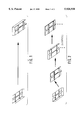
- FIG. 1 shows the usual manufacture of a nickel sheet by means of electroforming.
- FIG. 2 shows the manufacture of a nickel sheet by electroforming by means of a multiple-copying method.
- FIG. 3 shows the unprocessed nickel sheet, not stress-free, before the magnetic clamping.
- FIG. 4 shows the magnetically clamped nickel sheet.
- FIG. 5 shows the worked nickel sheet before mounting in a shaping tool.
- FIG. 6 shows the protection of the micropattern by lacquer.
- FIG. 1 shows the conventional manufacture of an electroformed nickel sheet (nickel shim), provided with micropatterns, from a master pattern in "thick” electroplating.
- nickel sheet nickel shim
- Such a nickel sheet is 3-6 mm thick, not flexible, and is produced by an extremely stress-free galvanic process, with a total duration for the electroforming of several weeks.
- the shim planarity in the pattern zone is ⁇ 20 ⁇ m. Because of the duration of the electroforming process, and also for reasons of quality, this method is not suitable for producing multiple copies.
- nickel sheet 1 electroformed from the master pattern and provided with recessed micropatterns 4, is curved, i.e., is not free of stress, and is not even of uniform thickness.
- the nickel sheet, still curved in FIG. 3, is held under magnetic forces against a magnetic clamping block (plane mounting table 2) which has been ground absolutely plane, magnet 2 having to be able to draw the nickel sheet in all regions onto its surface.
- the clamping is carried out in such a way that the pattern side of the nickel sheet points toward the magnetic surface of the magnet.
- a prerequisite for this is a sheet which is not too thick (under approximately 1.5 mm).
- nickel sheets 1 with the recessed micropattern regions are pretreated for the grinding process, in that a drop of a lacquer 3, e.g., polymethyl acrylate, which is removable again later, dissolved in, e.g., ethyl acetate, is dripped into recess 4 in such a way that the bottom of the recess, as well as the micropatterns, are completely covered (FIG. 6).
- a lacquer 3 e.g., polymethyl acrylate
- micropattern After drying, the micropattern is protected from damage during the grinding process, e.g., from metallic grinding dust or liquid grinding material.
- Metal sheet 1 is clamped onto magnet 2 in such a way that micropatterns 4 point toward magnet 2.
- the back side of the metal sheet is then mechanically processed in such a way that metal sheet 1 assumes a plane-parallel shape. This can be effected with a geometrically undefined cutting edge (grinding) or a geometrically defined cutting edge (milling, etc.), in particular with a surface grinding machine, a milling machine or a planing machine.
- FIG. 4 shows the processing direction of the grinding. After removal from the magnetic, plane mounting table, because of its stress, the worked, planarized nickel sheet resets again and assumes the curved shape according to FIG. 5.
- the protective lacquer 3 can be removed again, e.g., at 60° C. with chloroform.
- the front side of the sheet is very plane. Over 40 mm, irregularities of about 8 ⁇ m were measured.
- the reworked nickel sheet is suitable for plastic modelings, and, in particular, for injection molding, hot stamping or reaction casting methods. It can be used especially advantageously for producing integrated optical waveguide components, for example, in accordance with German Patent Nos. P 44 01 219.5 or P 196 19 353.2, as well as for all other plane micropatterns.
- an electromagnetic plane mounting table can be used instead of a magnetic plane mounting table having a permanent magnet.
Landscapes
- Engineering & Computer Science (AREA)
- Mechanical Engineering (AREA)
- Electroplating Methods And Accessories (AREA)
- Moulds For Moulding Plastics Or The Like (AREA)
Abstract
Description
Claims (8)
Applications Claiming Priority (2)
| Application Number | Priority Date | Filing Date | Title |
|---|---|---|---|
| DE19626215A DE19626215A1 (en) | 1996-06-29 | 1996-06-29 | Process for the post-processing of an electroplated magnetic metal sheet |
| DE19626215 | 1996-06-29 |
Publications (1)
| Publication Number | Publication Date |
|---|---|
| US5926938A true US5926938A (en) | 1999-07-27 |
Family
ID=7798451
Family Applications (1)
| Application Number | Title | Priority Date | Filing Date |
|---|---|---|---|
| US08/858,986 Expired - Fee Related US5926938A (en) | 1996-06-29 | 1997-05-20 | Method for working an electroformed magnetic metal sheet |
Country Status (3)
| Country | Link |
|---|---|
| US (1) | US5926938A (en) |
| EP (1) | EP0816535B1 (en) |
| DE (2) | DE19626215A1 (en) |
Cited By (2)
| Publication number | Priority date | Publication date | Assignee | Title |
|---|---|---|---|---|
| US20080290635A1 (en) * | 2007-05-24 | 2008-11-27 | Wieczorek Joseph P | Continuous side airbag seam |
| US10974353B2 (en) * | 2017-06-22 | 2021-04-13 | Hs Marston Aerospace Limited | Method of forming a component for a heat exchanger |
Families Citing this family (1)
| Publication number | Priority date | Publication date | Assignee | Title |
|---|---|---|---|---|
| US20120220678A1 (en) | 2009-11-03 | 2012-08-30 | Christof Mehler | Thermoplastic compositions having improved flowability |
Citations (2)
| Publication number | Priority date | Publication date | Assignee | Title |
|---|---|---|---|---|
| US3801293A (en) * | 1972-06-05 | 1974-04-02 | Timesavers Inc | Method of machining ferromagnetic workpieces to true flatness |
| EP0660315A1 (en) * | 1993-12-24 | 1995-06-28 | Canon Kabushiki Kaisha | Process and apparatus for production of a stamper |
-
1996
- 1996-06-29 DE DE19626215A patent/DE19626215A1/en not_active Withdrawn
-
1997
- 1997-03-04 DE DE59704423T patent/DE59704423D1/en not_active Expired - Fee Related
- 1997-03-04 EP EP97103499A patent/EP0816535B1/en not_active Expired - Lifetime
- 1997-05-20 US US08/858,986 patent/US5926938A/en not_active Expired - Fee Related
Patent Citations (2)
| Publication number | Priority date | Publication date | Assignee | Title |
|---|---|---|---|---|
| US3801293A (en) * | 1972-06-05 | 1974-04-02 | Timesavers Inc | Method of machining ferromagnetic workpieces to true flatness |
| EP0660315A1 (en) * | 1993-12-24 | 1995-06-28 | Canon Kabushiki Kaisha | Process and apparatus for production of a stamper |
Cited By (2)
| Publication number | Priority date | Publication date | Assignee | Title |
|---|---|---|---|---|
| US20080290635A1 (en) * | 2007-05-24 | 2008-11-27 | Wieczorek Joseph P | Continuous side airbag seam |
| US10974353B2 (en) * | 2017-06-22 | 2021-04-13 | Hs Marston Aerospace Limited | Method of forming a component for a heat exchanger |
Also Published As
| Publication number | Publication date |
|---|---|
| EP0816535A1 (en) | 1998-01-07 |
| DE19626215A1 (en) | 1998-01-02 |
| DE59704423D1 (en) | 2001-10-04 |
| EP0816535B1 (en) | 2001-08-29 |
Similar Documents
| Publication | Publication Date | Title |
|---|---|---|
| AU683521B2 (en) | Method for reproducing holograms, kinoforms, diffractive optical elements, microstructures, and a plastic binary optical element produced by such a method | |
| GB1208943A (en) | Method and apparatus for generating a lens | |
| GB2076727A (en) | Making cast ophthalmic lenses | |
| EP1603705B1 (en) | Methods of making microstructured laminae | |
| CN106239835B (en) | A kind of manufacturing method of the smooth surface mold insert of injection mold | |
| CA2420648A1 (en) | Method of fabricating an injection mold insert for molding lens molds | |
| US5926938A (en) | Method for working an electroformed magnetic metal sheet | |
| JP2000301550A (en) | Manufacturing method of micro lens array | |
| US20060005914A1 (en) | Method for machining a blank or semi-finished product of a future optical element | |
| US3815294A (en) | Method for making one-piece multifocal lenses | |
| US3840977A (en) | Method of making molds for molding or casting optical parts and the like | |
| CA2099769A1 (en) | Tool and method for forming a lens | |
| US12221711B2 (en) | Method for accelerated production of electroform tooling inserts | |
| GB2104824A (en) | Improvements in injection mould cavity surfaces | |
| JPH06284B2 (en) | Electric discharge machine | |
| JP2002200519A (en) | Cross groove processing method, mold and optical element | |
| CN101378878A (en) | Polishing of optical and non-optical tools for improved mold flow | |
| GB2230983A (en) | Lens blank mountings | |
| US6560848B2 (en) | Method for forming micro groove on mold used at PDP partition manufacture | |
| JPS58149167A (en) | Manufacture of fluidized abrasive grain work jig | |
| JPH11156628A (en) | Optical transmission surface treatment method for rod-shaped optical transmission bodies | |
| JP2005296828A (en) | Die head for coating | |
| Wu et al. | High productive technique for polishing free surface with elastic ball type wheel on grinding center | |
| CN118578530A (en) | Processing method of semiconductor thin-walled parts and annular thin-walled parts | |
| JP2002326148A (en) | Compound curved surface polishing method |
Legal Events
| Date | Code | Title | Description |
|---|---|---|---|
| AS | Assignment |
Owner name: ROBERT BOSCH GMBH, GERMANY Free format text: ASSIGNMENT OF ASSIGNORS INTEREST;ASSIGNORS:JAREK, MATHIAS;POTT, WOLFGANG;KRAGL, HANS;REEL/FRAME:008572/0365;SIGNING DATES FROM 19970421 TO 19970423 |
|
| FEPP | Fee payment procedure |
Free format text: PAYOR NUMBER ASSIGNED (ORIGINAL EVENT CODE: ASPN); ENTITY STATUS OF PATENT OWNER: LARGE ENTITY |
|
| AS | Assignment |
Owner name: HARTING ELKTRO-OPTISCHE BAUTEILE GMBH & CO. KG, GE Free format text: ASSIGNMENT OF ASSIGNORS INTEREST;ASSIGNOR:ROBERT BOSCH GMBH;REEL/FRAME:009570/0310 Effective date: 19981019 |
|
| FEPP | Fee payment procedure |
Free format text: PAYOR NUMBER ASSIGNED (ORIGINAL EVENT CODE: ASPN); ENTITY STATUS OF PATENT OWNER: LARGE ENTITY Free format text: PAYER NUMBER DE-ASSIGNED (ORIGINAL EVENT CODE: RMPN); ENTITY STATUS OF PATENT OWNER: LARGE ENTITY |
|
| FPAY | Fee payment |
Year of fee payment: 4 |
|
| REMI | Maintenance fee reminder mailed | ||
| LAPS | Lapse for failure to pay maintenance fees | ||
| LAPS | Lapse for failure to pay maintenance fees |
Free format text: PATENT EXPIRED FOR FAILURE TO PAY MAINTENANCE FEES (ORIGINAL EVENT CODE: EXP.); ENTITY STATUS OF PATENT OWNER: LARGE ENTITY |
|
| STCH | Information on status: patent discontinuation |
Free format text: PATENT EXPIRED DUE TO NONPAYMENT OF MAINTENANCE FEES UNDER 37 CFR 1.362 |
|
| FP | Lapsed due to failure to pay maintenance fee |
Effective date: 20070727 |