US5814237A - Method for forming deflection grating - Google Patents
Method for forming deflection grating Download PDFInfo
- Publication number
- US5814237A US5814237A US08/721,337 US72133796A US5814237A US 5814237 A US5814237 A US 5814237A US 72133796 A US72133796 A US 72133796A US 5814237 A US5814237 A US 5814237A
- Authority
- US
- United States
- Prior art keywords
- dielectric layer
- deflection grating
- forming
- layer
- semiconductor substrate
- Prior art date
- Legal status (The legal status is an assumption and is not a legal conclusion. Google has not performed a legal analysis and makes no representation as to the accuracy of the status listed.)
- Expired - Lifetime
Links
- 238000000034 method Methods 0.000 title claims abstract description 26
- 229920002120 photoresistant polymer Polymers 0.000 claims abstract description 48
- 239000000758 substrate Substances 0.000 claims abstract description 26
- 239000004065 semiconductor Substances 0.000 claims abstract description 25
- 230000003287 optical effect Effects 0.000 claims abstract description 17
- 238000001093 holography Methods 0.000 claims abstract description 14
- 150000001875 compounds Chemical class 0.000 claims abstract description 4
- 238000005530 etching Methods 0.000 claims abstract description 4
- 238000000059 patterning Methods 0.000 claims abstract description 3
- 238000001020 plasma etching Methods 0.000 claims description 17
- 238000005229 chemical vapour deposition Methods 0.000 claims description 4
- 150000004767 nitrides Chemical class 0.000 claims description 2
- 238000004528 spin coating Methods 0.000 claims description 2
- 238000010894 electron beam technology Methods 0.000 description 7
- 238000007796 conventional method Methods 0.000 description 6
- 238000001039 wet etching Methods 0.000 description 5
- 238000004891 communication Methods 0.000 description 4
- 238000011161 development Methods 0.000 description 2
- 230000018109 developmental process Effects 0.000 description 2
- 239000002184 metal Substances 0.000 description 2
- 229910052751 metal Inorganic materials 0.000 description 2
- 238000012545 processing Methods 0.000 description 2
- 230000002787 reinforcement Effects 0.000 description 2
- 238000000609 electron-beam lithography Methods 0.000 description 1
- 230000010355 oscillation Effects 0.000 description 1
- 230000007261 regionalization Effects 0.000 description 1
Images


Classifications
-
- G—PHYSICS
- G02—OPTICS
- G02B—OPTICAL ELEMENTS, SYSTEMS OR APPARATUS
- G02B5/00—Optical elements other than lenses
- G02B5/18—Diffraction gratings
- G02B5/1847—Manufacturing methods
- G02B5/1857—Manufacturing methods using exposure or etching means, e.g. holography, photolithography, exposure to electron or ion beams
-
- H—ELECTRICITY
- H01—ELECTRIC ELEMENTS
- H01S—DEVICES USING THE PROCESS OF LIGHT AMPLIFICATION BY STIMULATED EMISSION OF RADIATION [LASER] TO AMPLIFY OR GENERATE LIGHT; DEVICES USING STIMULATED EMISSION OF ELECTROMAGNETIC RADIATION IN WAVE RANGES OTHER THAN OPTICAL
- H01S5/00—Semiconductor lasers
- H01S5/10—Construction or shape of the optical resonator, e.g. extended or external cavity, coupled cavities, bent-guide, varying width, thickness or composition of the active region
- H01S5/12—Construction or shape of the optical resonator, e.g. extended or external cavity, coupled cavities, bent-guide, varying width, thickness or composition of the active region the resonator having a periodic structure, e.g. in distributed feedback [DFB] lasers
- H01S5/1231—Grating growth or overgrowth details
Definitions
- the present invention relates to a method for forming a deflection grating, and more particularly, to a method for forming a deflection grating of a distributed feedback laser diode (DFB-LD) used as a luminescent device in long distance communication.
- DFB-LD distributed feedback laser diode
- a method for forming a primary deflection grating for an InP group DFB-LD has been studied for a long time.
- InP group DFB-LD having an oscillation wavelength of 1.55 ⁇ m is used for long distance optical communication.
- the method for forming a deflection grating is roughly divided into optical holography and electron beam lithography according to a photoresist pattern formation method.
- the optical holography includes a wet etching method, and a method in which a metal like Cr or Ti is lifted off and reactive ion etching (RIE) is carried out using the metal.
- RIE reactive ion etching
- a fabricated deflection grating is triangular, and its depth cannot exceed 90 mm.
- an electron beam should be used in order to obtain the primary deflection grating. Accordingly, it takes much time to fabricate the primary deflection grating. Furthermore, for the method using the electron beam, it takes much time to directly draw the image of the deflection grating although it is able to control the shape of the deflection grating, and use RIE etching.
- FIGS. 1A and 1B show a conventional method for forming a deflection grating using the optical holography.
- a photoresist 13 is coated on an n-type InP semiconductor substrate 11, and exposed and developed through the optical holography to form a photoresist pattern 13, thereby selectively exposing semiconductor substrate 11.
- the photoresist is selectively exposed due to interference and reinforcement of light during the optical holography, the photoresist is patterned by the development.
- the exposed portion of semiconductor substrate 11 is isotropically etched through wet etching using photoresist pattern 13 as a mask, to form a deflection grating 15. Then, photoresist pattern 13 is removed.
- time required to fabricate the deflection grating is short.
- the deflection grating formed by wet etching is triangular, and its depth is limited to 800-1000 ⁇ . Also, it is difficult to control its duty rate.
- the semiconductor substrate is isotropically etched through wet etching, the deflection grating cannot be formed deeply.
- FIGS. 2A, 2B and 2C show another conventional method for forming a deflection grating using electron beam.
- a dielectric layer 23 and photoresist layer 25 are sequentially formed on an n-type InP semiconductor substrate 21. Photoresist layer 25 is exposed by an electron beam and developed to form photoresist pattern 25.
- a portion of dielectric layer 23 on which photoresist pattern 25 is not formed is selectively removed through RIE using photoresist pattern 25 as a mask, to selectively expose semiconductor substrate 21.
- the etch selectivity of dielectric layer 23 and photoresist layer 25 is controlled so as to etch dielectric layer 23 faster than photoresist layer 25. By doing so, photoresist pattern 25 is prevented from being damaged. Thereafter, photoresist pattern 25 is removed.
- a portion of semiconductor substrate 21 on which dielectric layer 23 is not formed is anisotropically etched through RIE using dielectric layer 23 as a mask, to form a deflection grating 27. Then, dielectric layer 23 is removed.
- deflection grating 27 is formed in a manner that the etch selectivity of dielectric layer 23 and substrate 21 is controlled so as to etch semiconductor substrate 21 faster than dielectric layer 23.
- the photoresist layer is exposed utilizing an electron beam and developed to form the photoresist pattern, and two-time RIE are carried out. Accordingly, the deflection grating has the vertical section, and its depth and duty rate can be optionally controlled.
- the photoresist since the photoresist is exposed through electron beam, it requires long processing time.
- a method for forming a deflection grating including the steps of: sequentially forming a dielectric layer and photoresist layer on a compound semiconductor substrate, and patterning the photoresist layer through optical holography to expose the dielectric layer; removing a portion of the dielectric layer on which the patterned photoresist layer is not formed, through RIE using the patterned photoresist layer as a mask; anisotropically etching a portion of the semiconductor substrate on which the dielectric layer is not formed, through RIE using the dielectric layer as a mask, to form a deflection grating; and removing the dielectric layer.
- FIGS. 1A and 1B are cross-sectional views showing a conventional method for forming a deflection grating, using optical holography
- FIGS. 2A, 2B and 2C are cross-sectional views showing another conventional method for forming a deflection grating, using an electron beam.
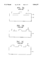
- FIGS. 3A, 3B and 3C are cross-sectional views showing a method for forming a deflection grating according to the present invention.
- FIGS. 3A, 3B and 3C are cross-sectional views showing a method for forming a deflection grating according to the present invention.
- a dielectric layer 33 and photoresist layer 35 are sequentially formed on an n-type InP semiconductor substrate 31.
- Dielectric layer 33 is formed in a manner that an oxide layer or nitride layer is formed by a thickness of 300 to 500 ⁇ through chemical vapor deposition (CVD).
- Photoresist layer 35 is formed by a thickness of 300 to 500 ⁇ through spin coating.
- Photoresist layer 35 is exposed through optical holography and developed to form a photoresist pattern 35. By doing so, dielectric layer 33 is selectively exposed.
- photoresist layer 35 is selectively exposed due to the interference and reinforcement of light during optical holography, photoresist layer 35 is patterned by the development.
- a portion of dielectric layer 33 on which photoresist pattern 35 is not formed is selectively removed through RIE using photoresist pattern 35 as a mask, to expose a portion of semiconductor substrate 31.
- RF power of the RIE apparatus is reduced but its chamber pressure is increased to control the etch selectivity of photoresist layer 35 and dielectric layer 33 to 1:4.
- dielectric layer 33 can be patterned without damaging photoresist pattern 35.
- photoresist pattern 35 is removed.
- the exposed portion of semiconductor substrate 31 is anisotropically etched through RIE using dielectric layer 33 as a mask, to form a deflection grating 37. Thereafter, dielectric layer 33 is removed.
- semiconductor substrate 31 is etched using CH 4 /H 2 to set the etch selectivity of dielectric layer 33 and semiconductor substrate 31 to 1:20, thereby preventing dielectric layer 33 from being damaged.
- deflection grating 37 has the vertical section. Also, dielectric layer 33 is prevented from being damaged so that the depth and duty ratio of deflection grating 37 can be easily controlled.
- the dielectric layer and photoresist layer are sequentially formed on the semiconductor substrate, and the photoresist layer is patterned through optical holography. Then, the dielectric layer is patterned through RIE using the patterned photoresist layer as a mask, and the semiconductor substrate is anisotropically etched through RIE using the dielectric layer as a mask to form the deflection grating. Thereafter, the dielectric layer is removed.
- the deflection grating has the vertical section, and its depth and duty ratio can be easily controlled.
Landscapes
- Physics & Mathematics (AREA)
- General Physics & Mathematics (AREA)
- Optics & Photonics (AREA)
- Engineering & Computer Science (AREA)
- Manufacturing & Machinery (AREA)
- Condensed Matter Physics & Semiconductors (AREA)
- Electromagnetism (AREA)
- Diffracting Gratings Or Hologram Optical Elements (AREA)
Abstract
Description
Claims (8)
Priority Applications (1)
| Application Number | Priority Date | Filing Date | Title |
|---|---|---|---|
| US08/721,337 US5814237A (en) | 1996-09-26 | 1996-09-26 | Method for forming deflection grating |
Applications Claiming Priority (1)
| Application Number | Priority Date | Filing Date | Title |
|---|---|---|---|
| US08/721,337 US5814237A (en) | 1996-09-26 | 1996-09-26 | Method for forming deflection grating |
Publications (1)
| Publication Number | Publication Date |
|---|---|
| US5814237A true US5814237A (en) | 1998-09-29 |
Family
ID=24897570
Family Applications (1)
| Application Number | Title | Priority Date | Filing Date |
|---|---|---|---|
| US08/721,337 Expired - Lifetime US5814237A (en) | 1996-09-26 | 1996-09-26 | Method for forming deflection grating |
Country Status (1)
| Country | Link |
|---|---|
| US (1) | US5814237A (en) |
Cited By (3)
| Publication number | Priority date | Publication date | Assignee | Title |
|---|---|---|---|---|
| US6331380B1 (en) * | 1997-12-12 | 2001-12-18 | Applied Materials, Inc. | Method of pattern etching a low K dielectric layer |
| US20070114923A1 (en) * | 2003-02-13 | 2007-05-24 | Samsung Sdi Co., Ltd. | Thin film electroluminescence display device and method of manufacturing the same |
| EP2199837A1 (en) * | 2008-12-16 | 2010-06-23 | Alcatel Lucent | A dispersion grating |
Citations (2)
| Publication number | Priority date | Publication date | Assignee | Title |
|---|---|---|---|---|
| US4927785A (en) * | 1987-06-04 | 1990-05-22 | U.S. Philips Corporation | Method of manufacturing semiconductor devices |
| EP0619602A2 (en) * | 1993-04-07 | 1994-10-12 | Sony Corporation | Semiconductor device and method for manufacturing semiconductor device |
-
1996
- 1996-09-26 US US08/721,337 patent/US5814237A/en not_active Expired - Lifetime
Patent Citations (2)
| Publication number | Priority date | Publication date | Assignee | Title |
|---|---|---|---|---|
| US4927785A (en) * | 1987-06-04 | 1990-05-22 | U.S. Philips Corporation | Method of manufacturing semiconductor devices |
| EP0619602A2 (en) * | 1993-04-07 | 1994-10-12 | Sony Corporation | Semiconductor device and method for manufacturing semiconductor device |
Cited By (4)
| Publication number | Priority date | Publication date | Assignee | Title |
|---|---|---|---|---|
| US6331380B1 (en) * | 1997-12-12 | 2001-12-18 | Applied Materials, Inc. | Method of pattern etching a low K dielectric layer |
| US20070114923A1 (en) * | 2003-02-13 | 2007-05-24 | Samsung Sdi Co., Ltd. | Thin film electroluminescence display device and method of manufacturing the same |
| US7455563B2 (en) * | 2003-02-13 | 2008-11-25 | Samsung Sdi Co., Ltd. | Thin film electroluminescence display device and method of manufacturing the same |
| EP2199837A1 (en) * | 2008-12-16 | 2010-06-23 | Alcatel Lucent | A dispersion grating |
Similar Documents
| Publication | Publication Date | Title |
|---|---|---|
| US6124080A (en) | Method of manufacturing an optical device with a groove accurately formed | |
| US5024726A (en) | Method for producing a λ/4 shift type diffraction grating | |
| US6344367B1 (en) | Method of fabricating a diffraction grating | |
| JPH07273404A (en) | Semiconductor laser diode manufacturing method | |
| US5814237A (en) | Method for forming deflection grating | |
| US5567552A (en) | Method for fabricating a phase shift mask | |
| EP0363547B1 (en) | Method for etching mirror facets of III-V semiconductor structures | |
| KR20050065745A (en) | Method for fabricating patterns of shallow trench isolation | |
| KR0169836B1 (en) | Method for forming diffraction grating | |
| US6524753B2 (en) | Method for manufacturing phase shift mask | |
| KR20010003465A (en) | method of forming fine pattern of semiconductor device | |
| US7195716B2 (en) | Etching process and patterning process | |
| JP2000193813A (en) | Method of forming diffraction grating, diffraction grating, and optical semiconductor device | |
| US20020028394A1 (en) | Method for manufacturing a membrane mask | |
| JPH11167037A (en) | Production of optical waveguide element utilizing induction coupling plasma apparatus | |
| KR100318462B1 (en) | Micro pattern gap formation method of semiconductor device | |
| JP2600588B2 (en) | Method of forming dry etching mask | |
| JPH05206085A (en) | Fine pattern formation method | |
| KR0140846B1 (en) | Method for wet etching for forming a grating | |
| US20040132273A1 (en) | Formation method of gate electrode in semiconductor | |
| KR100429849B1 (en) | Method for forming etch mask used in fabricating planar lightwave guide, especially preventing the damage of an epi layer like a mask pattern and a lightwave guide | |
| JPH0829606A (en) | Method for manufacturing phase shift diffraction grating | |
| JP2734951B2 (en) | Method for manufacturing semiconductor device | |
| KR20010060984A (en) | Manufacturing method for contact hole in semiconductor device | |
| US20020011678A1 (en) | Method and system for providing a robust alignment mark at thin oxide layers |
Legal Events
| Date | Code | Title | Description |
|---|---|---|---|
| AS | Assignment |
Owner name: ELECTRONICS AND TELECOMMUNICATIONS RESEARCH INSTIT Free format text: ASSIGNMENT OF ASSIGNORS INTEREST;ASSIGNOR:PARK, CHONG-DAE;REEL/FRAME:008245/0994 Effective date: 19960909 |
|
| AS | Assignment |
Owner name: CALIFORNIA INSTITUTE OF TECHNOLOGY, CALIFORNIA Free format text: ASSIGNMENT OF ASSIGNORS INTEREST;ASSIGNOR:KERN, ROGER G.;REEL/FRAME:008255/0033 Effective date: 19961118 |
|
| STCF | Information on status: patent grant |
Free format text: PATENTED CASE |
|
| FEPP | Fee payment procedure |
Free format text: PAYOR NUMBER ASSIGNED (ORIGINAL EVENT CODE: ASPN); ENTITY STATUS OF PATENT OWNER: LARGE ENTITY |
|
| FPAY | Fee payment |
Year of fee payment: 4 |
|
| FPAY | Fee payment |
Year of fee payment: 8 |
|
| FEPP | Fee payment procedure |
Free format text: PAYOR NUMBER ASSIGNED (ORIGINAL EVENT CODE: ASPN); ENTITY STATUS OF PATENT OWNER: LARGE ENTITY Free format text: PAYER NUMBER DE-ASSIGNED (ORIGINAL EVENT CODE: RMPN); ENTITY STATUS OF PATENT OWNER: LARGE ENTITY |
|
| FEPP | Fee payment procedure |
Free format text: PAYOR NUMBER ASSIGNED (ORIGINAL EVENT CODE: ASPN); ENTITY STATUS OF PATENT OWNER: LARGE ENTITY Free format text: PAYER NUMBER DE-ASSIGNED (ORIGINAL EVENT CODE: RMPN); ENTITY STATUS OF PATENT OWNER: LARGE ENTITY |
|
| FPAY | Fee payment |
Year of fee payment: 12 |
|
| FEPP | Fee payment procedure |
Free format text: PAYOR NUMBER ASSIGNED (ORIGINAL EVENT CODE: ASPN); ENTITY STATUS OF PATENT OWNER: LARGE ENTITY Free format text: PAYER NUMBER DE-ASSIGNED (ORIGINAL EVENT CODE: RMPN); ENTITY STATUS OF PATENT OWNER: LARGE ENTITY |