US5776816A - Nitride double etching for twin well align - Google Patents
Nitride double etching for twin well align Download PDFInfo
- Publication number
- US5776816A US5776816A US08/739,056 US73905696A US5776816A US 5776816 A US5776816 A US 5776816A US 73905696 A US73905696 A US 73905696A US 5776816 A US5776816 A US 5776816A
- Authority
- US
- United States
- Prior art keywords
- nitride
- layer
- oxide layer
- photoresist
- nitride pattern
- Prior art date
- Legal status (The legal status is an assumption and is not a legal conclusion. Google has not performed a legal analysis and makes no representation as to the accuracy of the status listed.)
- Expired - Fee Related
Links
- 150000004767 nitrides Chemical class 0.000 title claims abstract description 52
- 238000005530 etching Methods 0.000 title claims abstract description 14
- 238000000034 method Methods 0.000 claims abstract description 37
- 229920002120 photoresistant polymer Polymers 0.000 claims abstract description 29
- 239000000758 substrate Substances 0.000 claims abstract description 17
- 239000004065 semiconductor Substances 0.000 claims abstract description 14
- 150000002500 ions Chemical class 0.000 claims abstract description 13
- 238000004519 manufacturing process Methods 0.000 claims abstract description 13
- 238000001459 lithography Methods 0.000 claims abstract description 11
- 239000012535 impurity Substances 0.000 claims abstract description 7
- 239000011248 coating agent Substances 0.000 claims abstract 5
- 238000000576 coating method Methods 0.000 claims abstract 5
- 238000000059 patterning Methods 0.000 claims abstract 5
- 238000002513 implantation Methods 0.000 claims description 8
- QVGXLLKOCUKJST-UHFFFAOYSA-N atomic oxygen Chemical compound [O] QVGXLLKOCUKJST-UHFFFAOYSA-N 0.000 claims description 6
- 239000001301 oxygen Substances 0.000 claims description 6
- 229910052760 oxygen Inorganic materials 0.000 claims description 6
- 238000004518 low pressure chemical vapour deposition Methods 0.000 claims description 5
- 238000005468 ion implantation Methods 0.000 claims description 4
- ZOXJGFHDIHLPTG-UHFFFAOYSA-N Boron Chemical compound [B] ZOXJGFHDIHLPTG-UHFFFAOYSA-N 0.000 claims description 2
- OAICVXFJPJFONN-UHFFFAOYSA-N Phosphorus Chemical compound [P] OAICVXFJPJFONN-UHFFFAOYSA-N 0.000 claims description 2
- 230000003213 activating effect Effects 0.000 claims description 2
- 229910052796 boron Inorganic materials 0.000 claims description 2
- 229910052698 phosphorus Inorganic materials 0.000 claims description 2
- 239000011574 phosphorus Substances 0.000 claims description 2
- 206010037660 Pyrexia Diseases 0.000 claims 2
- OKZIUSOJQLYFSE-UHFFFAOYSA-N difluoroboron Chemical compound F[B]F OKZIUSOJQLYFSE-UHFFFAOYSA-N 0.000 claims 2
- 238000005229 chemical vapour deposition Methods 0.000 claims 1
- 230000001590 oxidative effect Effects 0.000 claims 1
- 238000012876 topography Methods 0.000 abstract description 6
- XUIMIQQOPSSXEZ-UHFFFAOYSA-N Silicon Chemical compound [Si] XUIMIQQOPSSXEZ-UHFFFAOYSA-N 0.000 description 5
- 229910052710 silicon Inorganic materials 0.000 description 5
- 239000010703 silicon Substances 0.000 description 5
- 230000003647 oxidation Effects 0.000 description 3
- 238000007254 oxidation reaction Methods 0.000 description 3
- IJGRMHOSHXDMSA-UHFFFAOYSA-N Atomic nitrogen Chemical compound N#N IJGRMHOSHXDMSA-UHFFFAOYSA-N 0.000 description 2
- QAOWNCQODCNURD-UHFFFAOYSA-N Sulfuric acid Chemical compound OS(O)(=O)=O QAOWNCQODCNURD-UHFFFAOYSA-N 0.000 description 2
- 239000007789 gas Substances 0.000 description 2
- 238000010884 ion-beam technique Methods 0.000 description 2
- 239000000376 reactant Substances 0.000 description 2
- XPDWGBQVDMORPB-UHFFFAOYSA-N Fluoroform Chemical compound FC(F)F XPDWGBQVDMORPB-UHFFFAOYSA-N 0.000 description 1
- 229910003556 H2 SO4 Inorganic materials 0.000 description 1
- XMIJDTGORVPYLW-UHFFFAOYSA-N [SiH2] Chemical compound [SiH2] XMIJDTGORVPYLW-UHFFFAOYSA-N 0.000 description 1
- 238000006243 chemical reaction Methods 0.000 description 1
- 230000000694 effects Effects 0.000 description 1
- 238000002955 isolation Methods 0.000 description 1
- 239000000463 material Substances 0.000 description 1
- 229910052757 nitrogen Inorganic materials 0.000 description 1
- 238000001020 plasma etching Methods 0.000 description 1
- 229910021420 polycrystalline silicon Inorganic materials 0.000 description 1
- 229920005591 polysilicon Polymers 0.000 description 1
- 238000009751 slip forming Methods 0.000 description 1
- 238000000992 sputter etching Methods 0.000 description 1
Images


Classifications
-
- H—ELECTRICITY
- H10—SEMICONDUCTOR DEVICES; ELECTRIC SOLID-STATE DEVICES NOT OTHERWISE PROVIDED FOR
- H10D—INORGANIC ELECTRIC SEMICONDUCTOR DEVICES
- H10D84/00—Integrated devices formed in or on semiconductor substrates that comprise only semiconducting layers, e.g. on Si wafers or on GaAs-on-Si wafers
- H10D84/01—Manufacture or treatment
- H10D84/0123—Integrating together multiple components covered by H10D12/00 or H10D30/00, e.g. integrating multiple IGBTs
- H10D84/0126—Integrating together multiple components covered by H10D12/00 or H10D30/00, e.g. integrating multiple IGBTs the components including insulated gates, e.g. IGFETs
- H10D84/0165—Integrating together multiple components covered by H10D12/00 or H10D30/00, e.g. integrating multiple IGBTs the components including insulated gates, e.g. IGFETs the components including complementary IGFETs, e.g. CMOS devices
- H10D84/0191—Manufacturing their doped wells
-
- H—ELECTRICITY
- H10—SEMICONDUCTOR DEVICES; ELECTRIC SOLID-STATE DEVICES NOT OTHERWISE PROVIDED FOR
- H10D—INORGANIC ELECTRIC SEMICONDUCTOR DEVICES
- H10D84/00—Integrated devices formed in or on semiconductor substrates that comprise only semiconducting layers, e.g. on Si wafers or on GaAs-on-Si wafers
- H10D84/01—Manufacture or treatment
- H10D84/02—Manufacture or treatment characterised by using material-based technologies
- H10D84/03—Manufacture or treatment characterised by using material-based technologies using Group IV technology, e.g. silicon technology or silicon-carbide [SiC] technology
- H10D84/038—Manufacture or treatment characterised by using material-based technologies using Group IV technology, e.g. silicon technology or silicon-carbide [SiC] technology using silicon technology, e.g. SiGe
-
- Y—GENERAL TAGGING OF NEW TECHNOLOGICAL DEVELOPMENTS; GENERAL TAGGING OF CROSS-SECTIONAL TECHNOLOGIES SPANNING OVER SEVERAL SECTIONS OF THE IPC; TECHNICAL SUBJECTS COVERED BY FORMER USPC CROSS-REFERENCE ART COLLECTIONS [XRACs] AND DIGESTS
- Y10—TECHNICAL SUBJECTS COVERED BY FORMER USPC
- Y10S—TECHNICAL SUBJECTS COVERED BY FORMER USPC CROSS-REFERENCE ART COLLECTIONS [XRACs] AND DIGESTS
- Y10S438/00—Semiconductor device manufacturing: process
- Y10S438/975—Substrate or mask aligning feature
Definitions
- the present invention relates to the fabrication of alignment marks in a twin-well semiconductor device process, and more particularly it uses double nitride etching to manufacture the alignment marks.
- the field oxide isolation layer has a thickness of about 1000 to 3000 Angstroms above the silicon substrate, that can be used as the following polysilicon gate alignment marks.
- ASM stepper and Nikon stepper are the two most commonly used commercial steppers in today's semiconductor industry. Because the alignment methods of ASM stepper and Nikon stepper are different, one particular twin-well product can not use both ASM steppers and Nikon steppers for mass-production alignment. This phenomenon lowers the production line throughout. If we want to use ASM stepper alignment method in a Nillon stepper, it would need an extra photomask for zero layer alignment. Therefore, it will not only increase the number of manufacturing steps but also increase the production cost.
- the principle object of the present invention is to provide a method of fabricating the alignment marks in a twin-well semiconductor integrated circuits device process.
- the first oxide layer and the first nitride layer are formed in a P-type semiconductor substrate.
- the first photoresist layer is coated which is overlaying the first nitride layer.
- the first photoresist layer is patterned by conventional lithography technique to form an etching mask.
- the first nitride layer is patterned by plasma-etch technique.
- N- type ions are implanted into P-type substrate through the first oxide layer to form an N-doped region. After ion implantation, the first photoresist layer is removed.
- the second photoresist pattern is formed by conventional lithograph method again.
- the first nitride layer is partially plasma-etched to form the second nitride pattern where the second nitride pattern is located between N-well and P-well regions.
- P type ions are implanted into P-type substrate through the first oxide layer to form a P-doped region.
- the second photoresist layer is removed.
- the impurities in the N-doped and P-doped regions are thermally driven in a high-temperature environment to form the desired depths of N-well and P-well.
- an oxide layer is formed on the second nitride surface simutaneously. Therefore, the vertical height difference between the second nitride pattern and oxide can be used as alignment marks for the succeeding lithographic processes.
- the second oxide layer and the third nitride layer are formed.
- the third photoresist that can be used as etching mask for the third nitride layer is patterned by plasma-etch technology that leave some the second oxide layer uncovered.
- a field oxide region is formed by high-temperature oxidation of the uncovered the second oxide layer. Because the field oxide layer is symmetrically located between N-well and P-well regions, it can be used as an ideal alignment mark for lithography process. An effective alignment mark fabrication method that can use both ASM and Nikon steppers to have good control of critical dimension is then achieved.
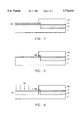
- FIGS. 1 through 11 schematically illustrate in cross sectional representation preferred embodiment of this invention.
- the invention discloses herein is directed to a method of fabricating twin-well alignment marks of integrated circuits.
- numerous details are set forth in order to provide a thorough understanding of the present invention. It will be obvious, however, to one skilled in the art of integrated circuits that these specific details need not be employed to practice the present invention. In other instance, well-known processing steps are not described in detail in order not unnecessarily obscure the present invention.
- the first pad oxide layer 5 that has a thickness of about 320 to 380 Angstroms is formed under 1000° C. thermal oxidation environment.
- the first nitride layer 5 that has a thickness of about 1350 to 1650 Angstroms is formed by low pressure chemical vapor deposition (LPCVD) technique under the following conditions: it has a base pressure of 350 mTorr, a temperature of 760° C., with reactant gases SiH 2 C1 2 and NH 3 flowing.
- LPCVD low pressure chemical vapor deposition
- the first photoresist layer 7 is selectively patterned by a conventional lithography method.
- the first nitride layer 5 is partially etched by plasmaetch technique to form the first nitride pattern 5A.
- the plasmaetch process can use magnetic enhanced reactive ion etching (MERIE), electron cyclotron etching (ECR), or conventional reaction ion etching (RIE) method. In present invention, it usually uses the MERIE method with reactant gases of CF 4 , CHF 3 , Ar and O 2 .
- N-type ion beams 9 are implanted into P-type silicon substrate 1 to form an N-doped region 11 as shown in FIG. 3.
- the N-type impurities that are ion implanted into P-type substrate are preferred to use Phosphorus (P 31 ), with an implantation energy of 50 to 150 keV, and an implantation dose of 10 11 to 10 13 cm -2 .
- the first photoresist layer 7 is stripped by oxygen plasma and sulfuric acid (H 2 SO 4 ). Then, the second photoresist layer 13 is coated then selectively patterned by lithography technique.
- the remaining first nitride pattern 5A is partially etched by using the second photoresist layer 13 to obtain the second nitride pattern 5B that is located in the middle of N-well and P-well junction.
- P-type ion beams 15 are implanted into the silicon substrate.
- the P-type impurities that are ion implanted into silicon substrate are preferred to use Boron (B 11 ) or borondiflouride (BF 2 ) ions, with an implantation energy of 10 to 80 keV, and an implantation dose of 10 12 to 10 13 cm -2 . Thereafter, the second photoresist 13 is removed.
- thermally drive-in in nitrogen and oxygen environment is carried out for the purpose of activating of impurities and obtaining the desired depths, to thereby form an N-well region 11A and P-well region 17A and thus a twin well.
- an oxide layer 19 that has a thickness of 2000 to 2400 Angstroms is simultaneously formed during the thermal drive-in process.
- the planer topography near the ladder 99 can be used as an alignment mark for the succeeding process that is the key point of the present invention.
- second pad oxide layer 21 and third nitride layer 23 are continuously formed overlying the twin well regions.
- the third photoresist regions 25 are selecting patterned by conventional lithography technique.
- the third nitride layer is etched by plasma-etch method to form the third nitride pattern 23A.
- a field oxide region 27 is formed in an oxygen environment with a temperature range of 925° to 975° C. for 150 to 200 minutes.
- the thickness of the field oxide region 27 is about 4000 to 6000 Angstroms.
- the field oxide region 27 that is symmetrically located between N-well and P-well regions has a smooth topography.
- the field oxide region 27 can be used as an ideal alignment mark for the succeeding lithographic steps that can reduce the number of processing steps so as to increase production through put.
Landscapes
- Exposure And Positioning Against Photoresist Photosensitive Materials (AREA)
- Exposure Of Semiconductors, Excluding Electron Or Ion Beam Exposure (AREA)
Abstract
Description
Claims (9)
Priority Applications (1)
| Application Number | Priority Date | Filing Date | Title |
|---|---|---|---|
| US08/739,056 US5776816A (en) | 1996-10-28 | 1996-10-28 | Nitride double etching for twin well align |
Applications Claiming Priority (1)
| Application Number | Priority Date | Filing Date | Title |
|---|---|---|---|
| US08/739,056 US5776816A (en) | 1996-10-28 | 1996-10-28 | Nitride double etching for twin well align |
Publications (1)
| Publication Number | Publication Date |
|---|---|
| US5776816A true US5776816A (en) | 1998-07-07 |
Family
ID=24970623
Family Applications (1)
| Application Number | Title | Priority Date | Filing Date |
|---|---|---|---|
| US08/739,056 Expired - Fee Related US5776816A (en) | 1996-10-28 | 1996-10-28 | Nitride double etching for twin well align |
Country Status (1)
| Country | Link |
|---|---|
| US (1) | US5776816A (en) |
Cited By (2)
| Publication number | Priority date | Publication date | Assignee | Title |
|---|---|---|---|---|
| US20070059914A1 (en) * | 2005-09-14 | 2007-03-15 | Hynix Semiconductor Inc. | Method of forming micro patterns in semiconductor devices |
| US20080016941A1 (en) * | 2004-06-24 | 2008-01-24 | Stephane Tisserand | Calibrating Device On A Silicon Substrate |
Citations (5)
| Publication number | Priority date | Publication date | Assignee | Title |
|---|---|---|---|---|
| US5252510A (en) * | 1991-05-03 | 1993-10-12 | Hyundai Electronics Industries Co., Ltd. | Method for manufacturing a CMOS device having twin wells and an alignment key region |
| US5256563A (en) * | 1992-04-16 | 1993-10-26 | Texas Instruments Incorporated | Doped well structure and method for semiconductor technologies |
| US5441902A (en) * | 1991-07-31 | 1995-08-15 | Texas Instruments Incorporated | Method for making channel stop structure for CMOS devices |
| US5460984A (en) * | 1989-09-11 | 1995-10-24 | Kabushiki Kaisha Toshiba | Method of manufacturing a semi conductor device having a second well formed within a first well |
| US5478762A (en) * | 1995-03-16 | 1995-12-26 | Taiwan Semiconductor Manufacturing Company | Method for producing patterning alignment marks in oxide |
-
1996
- 1996-10-28 US US08/739,056 patent/US5776816A/en not_active Expired - Fee Related
Patent Citations (5)
| Publication number | Priority date | Publication date | Assignee | Title |
|---|---|---|---|---|
| US5460984A (en) * | 1989-09-11 | 1995-10-24 | Kabushiki Kaisha Toshiba | Method of manufacturing a semi conductor device having a second well formed within a first well |
| US5252510A (en) * | 1991-05-03 | 1993-10-12 | Hyundai Electronics Industries Co., Ltd. | Method for manufacturing a CMOS device having twin wells and an alignment key region |
| US5441902A (en) * | 1991-07-31 | 1995-08-15 | Texas Instruments Incorporated | Method for making channel stop structure for CMOS devices |
| US5256563A (en) * | 1992-04-16 | 1993-10-26 | Texas Instruments Incorporated | Doped well structure and method for semiconductor technologies |
| US5478762A (en) * | 1995-03-16 | 1995-12-26 | Taiwan Semiconductor Manufacturing Company | Method for producing patterning alignment marks in oxide |
Cited By (4)
| Publication number | Priority date | Publication date | Assignee | Title |
|---|---|---|---|---|
| US20080016941A1 (en) * | 2004-06-24 | 2008-01-24 | Stephane Tisserand | Calibrating Device On A Silicon Substrate |
| US20070059914A1 (en) * | 2005-09-14 | 2007-03-15 | Hynix Semiconductor Inc. | Method of forming micro patterns in semiconductor devices |
| CN100416774C (en) * | 2005-09-14 | 2008-09-03 | 海力士半导体有限公司 | Method of forming micropatterns in semiconductor devices |
| US7575992B2 (en) | 2005-09-14 | 2009-08-18 | Hynix Semiconductor Inc. | Method of forming micro patterns in semiconductor devices |
Similar Documents
| Publication | Publication Date | Title |
|---|---|---|
| US8093155B2 (en) | Method of controlling striations and CD loss in contact oxide etch | |
| EP0313683A1 (en) | Method for fabricating a semiconductor integrated circuit structure having a submicrometer length device element | |
| US6274503B1 (en) | Etching method for doped polysilicon layer | |
| US4792534A (en) | Method of manufacturing a semiconductor device involving sidewall spacer formation | |
| JPS60124967A (en) | Integrated circuit structure | |
| US5045495A (en) | Forming twin wells in semiconductor devices | |
| JP3407023B2 (en) | Method for manufacturing semiconductor device | |
| US6391700B1 (en) | Method for forming twin-well regions of semiconductor devices | |
| US5776816A (en) | Nitride double etching for twin well align | |
| US5866447A (en) | Modified zero layer align method of twin well MOS fabrication | |
| US5814552A (en) | High step process for manufacturing alignment marks for twin-well integrated circuit devices | |
| US5946577A (en) | Method of manufacturing semiconductor device | |
| US20050164459A1 (en) | Soft-landing etching method using doping level control | |
| US6171897B1 (en) | Method for manufacturing CMOS semiconductor device | |
| US5688710A (en) | Method of fabricating a twin - well CMOS device | |
| US7125775B1 (en) | Method for forming hybrid device gates | |
| KR20010107707A (en) | Method for manufacturing semiconductor device having a sti structure | |
| KR100256237B1 (en) | How to Form Contact Holes | |
| CN1181625A (en) | A method of manufacturing alignment marks with high steps | |
| KR20010008839A (en) | Method of forming self-aligned contacts in semiconductor device | |
| CN1067801C (en) | integrated circuit manufacturing method | |
| KR100249012B1 (en) | Method for forming contact hole | |
| KR100200498B1 (en) | Device Separation Film of Semiconductor Device and Formation Method | |
| US20040033443A1 (en) | Method of manufacturing a semiconductor device | |
| JPH03283419A (en) | Semiconductor and manufacture thereof |
Legal Events
| Date | Code | Title | Description |
|---|---|---|---|
| AS | Assignment |
Owner name: HOLTEK MICROELECTRONICS,INC., TAIWAN Free format text: ASSIGNMENT OF ASSIGNORS INTEREST;ASSIGNOR:CHEN, CHWAN CHAO;REEL/FRAME:008287/0404 Effective date: 19961007 |
|
| AS | Assignment |
Owner name: UTEK SEMICONDUCTOR CORP., TAIWAN Free format text: CHANGE OF NAME;ASSIGNOR:HOLTEK MICROELECTRONICS, INC.;REEL/FRAME:009490/0001 Effective date: 19980630 |
|
| AS | Assignment |
Owner name: UNITED MICROELECTRONICS CORP., TAIWAN Free format text: ASSIGNMENT OF ASSIGNORS INTEREST;ASSIGNOR:UTEK SEMICONDUCTOR CORP.;REEL/FRAME:010568/0175 Effective date: 19991221 |
|
| FEPP | Fee payment procedure |
Free format text: PAYOR NUMBER ASSIGNED (ORIGINAL EVENT CODE: ASPN); ENTITY STATUS OF PATENT OWNER: LARGE ENTITY |
|
| FPAY | Fee payment |
Year of fee payment: 4 |
|
| REMI | Maintenance fee reminder mailed | ||
| LAPS | Lapse for failure to pay maintenance fees | ||
| STCH | Information on status: patent discontinuation |
Free format text: PATENT EXPIRED DUE TO NONPAYMENT OF MAINTENANCE FEES UNDER 37 CFR 1.362 |
|
| FP | Lapsed due to failure to pay maintenance fee |
Effective date: 20060707 |