BACKGROUND OF THE INVENTION
1. Field of the Invention
The present invention relates to a semiconductor memory device and more particularly to a semiconductor memory device including burn-in test circuitry. The present application is based upon Korean Application No. 30735/1995 which is incorporated herein by reference.
2. Description of the Related Art
Recently, with the development of high density semiconductor memory devices, methods and programs have been studied for reducing required device test time. To reduce test time, various burn-in circuits and methods have been developed.
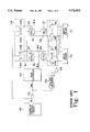
FIG. 1 is a circuit diagram used for testing the defective conditions of memory cells in a conventional semiconductor memory device. Referring to FIG. 1, a plurality of cells 106 store data. A plurality of bit line pairs BL and BLB are connected to the left and right sides of the cells 106, respectively and a plurality of word lines WL1 to WL8 are connected to upper and lower sides of the cells 106.
A precharge circuit 104 includes PMOS transistors 105A and 105B and is connected to a first terminal on each of the bit line pairs BL and BLB. A column pass circuit 107 includes transmission gates connected to a second terminal on each of the bit line pairs BL and BLB. Write drivers 110 and 111 are connected to the output terminals on the column pass circuit and perform write operations. A row decoder 102 applies a row signal to the cells 106 through the word lines WL1 to WL8 and a column decoder 103 applies column signals Y to the column pass circuit 107.
A burn-in control circuit 100 applies a burn-in control signal BI to the precharge circuit 104. The signal BI is delayed forming the signal BI' before reaching the precharge circuit 104. A complementary burn-in control signal BIB (which is inverted by an inverter 101 ) is applied to the row decoder 102 and a column decoder 103. The above-mentioned cells 106 are typically 8-bit cells or 16-bit cells. The PMOS transistors 105A and 105B are called "clamp transistors", hereinafter.
FIG. 2 is a timing diagram of the burn-in control signals in FIG. 1. Referring to FIGS. 1 and 2, the burn-in control circuit 100 is in a normal mode when the output BI and accordingly BI' are in a logic "low" level. The burn-in control circuit 100 is in a burn-in mode when the burn-in control signal BI and BI' are in a logic "high" level.
When the burn-in control signal BI' is in a logic "high level", two or more row signals WL1˜WL8 or column signals Y are concurrently selected, and the plurality of cells are enabled for a given time. Simultaneously selecting a plurality of cells 106 reduces the required burn-in time and achieves a high burn-in effect. If many column signals are enabled when the plurality of cells 106 are selected, a high current passes through the clamp transistors 105A and 105B in the precharge circuit 104 to the bit lines BL and BLB. The high current flows to the cells 106 and the write drivers 110 and 111, affecting the device.
To protect the device, the burn-in mode is entered. During the burnin mode, the burn-in control signal BI is in the logic "high" level and the clamp transistors 105A and 105B are turned "off", thereby preventing current from flowing.
The delay in BI' causes the row signals WL1˜WL8 or column signal Y to become enabled before the clamp transistors 105A and 105B are turned "off". During transitions to normal mode (BI'=logic "low" level), the clamp transistors 105A and 105B are turned "on" while the burn-in control signal BIB is still in the logic "low" level. Since the row signals WL1˜WL8 and column signal Y remain in the burn-in mode, a high current flows through the clamp transistors 105A and 105B and the write drivers 110 and 111. In other words, the burn-in control signal BI' and the complementary burn-in control signal BIB are enabled at the same time for intervals T1 and T2. The simultaneous enablement of BI' and BIB generates overcurrent flow.
SUMMARY OF THE INVENTION
Therefore, it is an object of the present invention to provide a semiconductor memory device burn-in test circuit that prevents overcurrent flow when changing between a burn-in mode and a normal mode.
A burn-in test circuit according to the invention applies a test signal that determines the defective status of memory cells in a memory circuit. The test circuit applies a signal that selects memory cells and enables a precharge circuit at predetermined time intervals that ensure no overcurrent conditions occur in the memory device while transitioning between normal and burn-in test modes.
BRIEF DESCRIPTION OF THE DRAWINGS
A more complete appreciation of this invention, and many of the advantages thereof, will be readily apparent by reference to the following detailed description when considered in conjunction with the accompanying drawings.
FIG. 1 is a prior art schematic circuit diagram of a prior art burn-in test circuit used for testing memory cells in a conventional semiconductor memory device.
FIG. 2 is a timing diagram of burn-in control signals generated by the circuit shown in FIG. 1;
FIG. 3 is a schematic circuit diagram of a burn-in test circuit according to the present invention; and
FIG. 4 is a timing diagram of control signals generated by the burn-in test circuit shown in FIG. 3.
DETAILED DESCRIPTION OF THE PREFERRED EMBODIMENT
FIG. 3 is a circuit diagram for testing memory cells according to the present invention. A control circuit 120 is connected between the burn-in control circuit 100 and the precharge circuit 104 and the row and column decoders 102 and 103. The control circuit 120 performs a delay operation during transitions between a burn-in mode and a normal mode.
The control circuit 120 includes a first controller which is connected between the burn-in control circuit 100 and the precharge circuit 104. The first controller generates the burn-in control signal BI' which is delayed in relation to the burn-in control signal BI output from the burn-in control circuit 100.
A second controller is connected between the burn-in control circuit 100 and the row and column decoders 102 and 103. The second controller generates the complementary burn-in control signal BIB in response to the burn-in control signal BI output from the burn-in control circuit 100.
The first controller includes a NAND gate 115 having a first input terminal receiving the burn-in control signal BI through an inverter 112. A second input terminal receives a delayed burn-in control signal BI from inverter 112 through a first delay circuit 113.
The second controller includes a NAND gate 116 having a first input terminal coupled to the burn-in control signal BI and a second input terminal coupled through a second delay circuit 114 to the burn-in control signal BI.
FIG. 4 is a timing diagram showing the burn-in control signals generated by the control circuit 120 according to the present invention. Referring to FIGS. 3 and 4, the burn-in control signal BI' output from the first controller is changed from a logic "low" level to a logic "high" level. The normal mode (BI'=logic "low" signal) changes to the burn-in mode (BI'=logic "high" signal) and the burn-in control signal BI' is transmitted without a delay to the precharge circuit 104. The transmitted burn-in control signal BI' causes the clamp transistors 105A and 105B within the precharge circuit 104 to turn "off". Conversely, the complementary burn-in control signal BIB which changes the row signals WL1˜WL8 and the column signal Y from the normal mode to the burn-in mode, is transmitted through the second delay circuit 114. The row signals WL1˜WL8 and the column signal Y are delayed when changing to the burn-in mode. Since the row signal and column signal are only enabled for burn-in mode after the clamp transistors 105A and 105B are shut off, overcurrent paths are prevented from being formed.
If the memory device is switched from the burn-in mode to the normal mode, the burn-in control signal BI' changes from the logic "high" level to the logic "low" level. Accordingly, the complementary burn-in control signal BIB changes logic level independently of the delay circuit 114. Thus, the complementary burn-in control signal BIB immediately changes the row signals WL1˜WL8 or the column signal Y to the normal mode. The burn-in control signal BI', however, is delayed by the first "On". delay circuit 113 before the clamp transistors 105A and 105B are turned
The clamp transistors 105A and 105B are turned "off" during the burn-in mode while the row signals or the column signals are continuously selected or simultaneously enabled. The clamp transistors 105A and 105B are turned "on" during the normal mode, and only one of the row signals or the column signals is selected.
The predetermined intervals T3 and T4 created by the control circuit 120 prevent the continuous or simultaneously enabled row and column signals from generating overcurrent conditions since the precharge circuit 104 converts from normal mode to burn-in mode before the column and row signals are enabled and converts back to normal mode after the column and row signals have already converted back to normal mode.
As set forth in the foregoing, the present invention provides a burn-in test system that prevents undesirable overcurrent conditions.
While the present invention has been described above with reference to the preferred embodiment, it will be appreciated by those skilled in the art that various substitutions and modifications can be made without departing from the spirit and scope of the invention as set forth in the following claims.