US5633600A - Output buffer circuit having a minimized output voltage propagation - Google Patents

Output buffer circuit having a minimized output voltage propagation Download PDF

Info

Publication number
US5633600A
US5633600A US08/536,780 US53678095A US5633600A US 5633600 A US5633600 A US 5633600A US 53678095 A US53678095 A US 53678095A US 5633600 A US5633600 A US 5633600A
Authority
US
United States
Prior art keywords
capacitor
channel transistor
output
input terminal
level
Prior art date
Legal status (The legal status is an assumption and is not a legal conclusion. Google has not performed a legal analysis and makes no representation as to the accuracy of the status listed.)
Expired - Fee Related
Application number
US08/536,780
Inventor
Yasuhiro Ohnishi
Current Assignee (The listed assignees may be inaccurate. Google has not performed a legal analysis and makes no representation or warranty as to the accuracy of the list.)
NEC Corp
Original Assignee
NEC Corp
Priority date (The priority date is an assumption and is not a legal conclusion. Google has not performed a legal analysis and makes no representation as to the accuracy of the date listed.)
Filing date
Publication date
Application filed by NEC Corp filed Critical NEC Corp
Assigned to NEC CORPORATION reassignment NEC CORPORATION ASSIGNMENT OF ASSIGNORS INTEREST (SEE DOCUMENT FOR DETAILS). Assignors: OHNISHI, YASUHIRO
Application granted granted Critical
Publication of US5633600A publication Critical patent/US5633600A/en
Anticipated expiration legal-status Critical
Expired - Fee Related legal-status Critical Current

Links

Images

Classifications

    • HELECTRICITY
    • H03ELECTRONIC CIRCUITRY
    • H03KPULSE TECHNIQUE
    • H03K17/00Electronic switching or gating, i.e. not by contact-making and –breaking
    • H03K17/16Modifications for eliminating interference voltages or currents
    • H03K17/161Modifications for eliminating interference voltages or currents in field-effect transistor switches
    • H03K17/162Modifications for eliminating interference voltages or currents in field-effect transistor switches without feedback from the output circuit to the control circuit
    • HELECTRICITY
    • H03ELECTRONIC CIRCUITRY
    • H03KPULSE TECHNIQUE
    • H03K4/00Generating pulses having essentially a finite slope or stepped portions

Definitions

  • the present invention relates to an output buffer circuit, and more specifically to an output buffer circuit composed of MOS transistors (metal-oxide-semiconductor field effect transistors) and for use in an integrated circuit.
  • MOS transistors metal-oxide-semiconductor field effect transistors
  • the slew rate output buffer in a MOSIC is a buffer in which an output waveform changes at a low speed when an buffer output changes front a high level to a low level or vice versa, in order to avoid all of MOS transistors driving an output terminal, from being put into an ON condition simultaneously.
  • This output buffer function is effective in preventing generation of noises on a voltage supply line or a ground line in the MOSIC, and also in preventing an overshooting or an undershooting from occurring in the output voltage waveform of the output buffer.
  • FIG. 1 there is shown a circuit diagram illustrating one example of a conventional slew rate output buffer circuit in a CMOS (complementary MOS transistor) technology.
  • the shown buffer circuit basically includes an output driving stage composed of a P-channel transistor 310 and an N-channel transistor 311 having their drain electrode connected in common to an output terminal 312.
  • the P-channel transistor 310 has a source electrode connected to a voltage supply line VDD and a gate electrode connected to one end of a capacitor 308, the other end of which is connected to the voltage supply line VDD.
  • the N-channel transistor 311 has a source electrode connected to a ground line and a gate electrode connected to one end of a capacitor 309, the other end of which is connected to the ground line.
  • each of the capacitors 308 and 309 includes a capacitance of the gate electrode of the MOS transistor connected with the capacitor concerned.
  • An input terminal 301 is connected to an input of each of inverters 302 and 303, which cooperate with the input terminal to control a charging/discharging timing of the capacitors 308 and 309.
  • an output of the inverter 302 is connected through a resistor 304 to the one end of the capacitor 308 so as to charge the capacitor 308 to a ground level.
  • a P-channel transistor 306 having its gate connected to the input terminal 301, its source connected to the voltage supply line VDD and its drain connected to the one end of the capacitor 308, acts to discharge the capacitor 308 to a voltage supply level.
  • An output of the inverter 303 is connected through a resistor 305 to the one end of the capacitor 309 so as to charge the capacitor 309 to the voltage supply level.
  • An N-channel transistor 307 having its gate connected to the input terminal 301, its source connected to the ground line and its drain connected to the one end of the capacitor 309, acts to discharge the capacitor 309 to ground level.
  • FIG. 2 illustrates waveforms on various points in the circuit shown in FIG. 1.
  • the P-channel transistor 306 When an input voltage applied to the input terminal 301 is a low level, the P-channel transistor 306 is on, so that the capacitor 308 is in a condition discharged to the voltage supply level.
  • the N-channel transistor 307 is off, so that the capacitor 309 is in a condition charged to the voltage supply level through the resistor 305 from the output of the inverter 303. Therefore, the output driving P-channel transistor 310 is off and the output driving N-channel transistor 311 is on, so that an voltage on the output terminal 312 is at a ground level.
  • the output of the inverter 303 changes to the ground level, and simultaneously, the N-channel transistor 307 is brought from the off condition to the on condition, so that the capacitor 309 is discharged to the ground level, and therefore, the output driving N-channel transistor 311 is immediately turned off.
  • the P-channel transistor 306 is brought from the on condition to the off condition, and simultaneously, the output of the inverter 302 changes to the ground level.
  • the capacitor 308 is charged by the output of the inverter 302 through the resistor 304 towards the ground level, the potential on the one end of the capacitor 308 gradually shifts to the ground level. Therefore, the output voltage on the output terminal 312 slowly rises up with a substantial rising time.
  • the capacitor 308 is discharged to the voltage supply level, so that the output driving P-channel transistor 310 is immediately turned off. But, the capacitor 309 is charged through the resistor 305, the potential of the capacitor 309 gradually shifts towards the voltage supply level. Accordingly, the output voltage on the output terminal 312 slowly falls down with a substantial rising time.
  • FIG. 3 there is shown a circuit diagram of another conventional output buffer circuit shown in FIG. 2 of Japanese Patent Application Laid-open Publication No. JP-A-2-122725.
  • the output buffer circuit shown in FIG. 3 is configured to be capable of selecting the rising time and the failing time between a high speed value and a low speed value by means of a control terminal 502 in accordance with an application thereof.
  • both of the N-channel transistor 507 and the P-channel transistor 508 are on.
  • An N-channel transistor 506 and a P-channel transistor 509 cooperate with the inverters 503 and 505, respectively, to drive the gate of the output driving P-channel transistor 510 and the output driving N-channel transistor 511 with a large drive power, so as to turn on the output driving transistor with a high driving speed. Therefore, the output voltage of the output terminal 512 has a high rising time and a high falling time.
  • the above mentioned conventional output buffer circuits are so designed that, in order to make slow the rising and the falling of the output voltage on the output terminal, the capacitor means including a gate capacitance of the output driving MOS transistor is gradually charged through a resistor means, so as to turn on the output driving MOS transistor at a low speed.
  • Another object of the present invention is to provide an output buffer circuit having an output voltage having a slow rising/falling time but capable of minimizing the output voltage propagation delay time.
  • an output buffer circuit comprising an input terminal, an output terminal, an output driving MOS transistor having a drain electrode and a source electrode, one of which is connected to the output terminal, the output driving MOS transistor having a gate electrode for controlling an on/off of the output driving MOS transistor, a capacitor means connected to the gate of the output driving MOS transistor, a resistor means for charging the capacitor means when a potential on the input terminal is at a first signal level of turning on the output driving MOS transistor, a discharging switch means for discharging me capacitor means when the potential on the input terminal is at a second signal level of turning off the output driving MOS transistor, and a threshold voltage charging means for rapidly charging the capacitor means to a threshold voltage level of the output driving MOS transistor when the potential on the input terminal is at the first signal level of turning on the output driving MOS transistor.
  • FIG. 1 is a circuit diagram illustrating one example of a conventional slew rate output buffer circuit in a CMOS technology
  • FIG. 2 illustrates waveforms on various points in the circuit shown in FIG. 1;
  • FIG. 3 is a circuit diagram of another conventional output buffer circuit
  • FIG. 4 is a circuit diagram of an embodiment of the output buffer circuit in accordance with the present invention.
  • FIG. 5 illustrates waveforms on various points in the circuit shown in FIG. 4.
  • FIG. 4 there is shown a circuit diagram of an embodiment of the output buffer circuit in accordance with the present invention.
  • the shown output buffer circuit in accordance with the present invention is based on the CMOS technology, and includes an output driving stage composed of a P-channel transistor 117 and an N-channel transistor 118 having their drain electrode connected in common to an output terminal 119.
  • the P-channel transistor 117 has a source electrode connected to a voltage supply line VDD and a gate electrode connected to one end of a capacitor 108, the other end of which is connected to the voltage supply line VDD.
  • the N-channel transistor 118 has a source electrode connected to a ground line and a gate electrode connected to one end of a capacitor 116, the other end of which is connected to the ground line.
  • each of the capacitors 108 and 116 includes a gate capacitance of the gate electrode of the MOS transistor connected with the capacitor concerned and also a wiring capacitance if any.
  • An input terminal 101 is connected to an input of each of inverters 102, 103 and 104, which cooperate with the input terminal 101 to control a charging/discharging timing of the capacitors 108 and 116.
  • An output of the inverter 102 is connected through a resistor 105 to the one end of the capacitor 108 so as to charge the capacitor 108 to a ground level.
  • a P-channel transistor 107 having its gate connected to the input terminal 101, its source connected to the voltage supply line VDD and its drain connected to the one end of the capacitor 108, acts to discharge the capacitor 108 to a voltage supply level of the voltage supply line VDD.
  • An output of the inverter 104 is connected through a resistor 106 to the one end of the capacitor 116 so as to charge the capacitor 116 to the voltage supply level.
  • An N-channel transistor 115 having its gate connected to the input terminal 101, its source connected to the ground line and its drain connected to the one end of the capacitor 116, acts to discharge the capacitor 116 to the ground level of the ground line.
  • the shown output buffer further includes a threshold voltage charging circuit I including a capacitor 110 and N-channel transistors 109 and III, and another threshold voltage charging circuit 2 including a capacitor 113 and P-channel transistors 114 and 112.
  • the N-channel transistor 109 has its gate connected to the input terminal 101, its source connected to one end of the capacitor 110 having its other end connected to the ground line, and its drain connected to the one end of the capacitor 108.
  • This N-channel transistor 109 acts as a switch for connecting the capacitor 110 to the capacitor 108.
  • the N-channel transistor 111 has its gate connected to an output of the inverter 103, its source connected to the ground line and its drain connected to the one end of the capacitor 110. This N-channel transistor 111 functions to precharge the capacitor 110 to the ground level.
  • the P-channel transistor 114 has its gate connected to the input terminal 101, its source connected to one end or the capacitor 113 having its other end connected to the voltage supply line VDD, and its drain connected to the one end of the capacitor 116.
  • This P-channel transistor 114 acts as a switch for connecting the capacitor 113 to the capacitor 116.
  • the P-channel transistor 112 has its gate connected to the output of the inverter 103, its source connected to the voltage supply line VDD and its drain connected to the one end of the capacitor 113. This P-channel transistor 112 functions to precharge the capacitor 113 to the voltage supply level.
  • FIG. 4 illustrates waveforms on various points in the circuit shown in FIG. 4.
  • the P-channel transistor 107 When an input voltage applied to the input terminal 101 is a low level, the P-channel transistor 107 is on, and the N-channel transistor 109 is off, so that the capacitor 108 is in a condition discharged to the voltage supply level. Simultaneously, the N-channel transistor 109 is on, so that the capacitor 110 is in a condition precharged to the ground level. On the other hand, the P-channel transistor 112 and the N-channel transistor 115 are off and the P-channel transistor 114 is on, so that the capacitor 116 and the capacitor 113 are in a condition charged to the voltage supply level through the resistor 106 from the output of the inverter 104.
  • the output driving P-channel transistor 117 is off and the output driving N-channel transistor 118 is on, so that an voltage on the output terminal 119 is at a ground level.
  • the N-channel transistor 114 When the input voltage of the input terminal 101 rises up from the low level to a high level, the N-channel transistor 114 is brought from the on condition to the off condition, and the output of the inverter 104 changes to the ground level, and simultaneously, the N-channel transistor 115 is brought from the off condition to the on condition, so that the capacitor 116 is discharged to the ground level, and therefore, the output driving N-channel transistor 118 is immediately turned off.
  • the P-channel transistor 107 is brought from the on condition to the off condition, and simultaneously, the output of the inverter 102 changes to the ground level so as to charge the capacitor 108 towards t&e ground level through the resistor 105.
  • the N-channel transistor 111 is brought from the on condition to the off condition, and simultaneously, the N-channel transistor 109 is brought from the off condition to the on condition, so that the capacitor 110 is connected to the capacitor 108.
  • electric charges precharged in the capacitor 110 is transferred to the capacitor 108, so that, as shown in FIG.
  • the potential on the capacitor 108 swiftly changes to an intermediate level which is between the voltage supply level and the ground level and which is determined by a ratio in a capacitance between the capacitor 108 and the capacitor 110. Thereafter, since the capacitor 108 and the capacitor 110 are charged through the resistor 105 from the output of the inverter 102, the potential on the one end of the capacitor 108 gradually shifts to the ground level.
  • the output driving P-channel transistor 117 when the input voltage had risen up, the output driving P-channel transistor 117 is quickly put in a condition just before the turning-on, and thereafter, gradually becomes the on condition. Accordingly, the output voltage of the output terminal 119 takes a voltage waveform having a long rising time (slow rising-up) but a minimized rising propagation delay time.
  • a circuit connected to the gate of the output driving P-channel transistor 117 and a circuit connected to the gate of the output driving N-channel transistor 118 operate in a complementary manner. Namely, the capacitor 108 is discharged to the voltage supply level, so that the output driving P-channel transistor 117 is immediately turned off.
  • the potential of the capacitor 116 is quickly changed to to an intermediate level which is between the voltage supply level and the ground level and which is determined by a ratio in a capacitance between the capacitor 116 and the capacitor 113, as shown in FIG. 5. Thereafter, since the capacitor 116 and the capacitor 113 are charged through the resistor 106, the potential of the capacitor 116 gradually shifts towards the voltage supply level.
  • the output driving N-channel transistor 118 when the input voltage had fallen down, the output driving N-channel transistor 118 is quickly put in a condition just before the turning-on, and thereafter, gradually becomes the on condition. Accordingly, the output voltage of the output terminal 119 takes a voltage waveform having a long falling time (slow falling-down) but a minimized falling propagation delay time.
  • the P-channel transistor 117 and the N-channel transistor are used to constitute the output driving stage, but it would be apparent to persons skilled in the an that the present invention can be equally applied to an output buffer including an output driving stage composed of only a single P-channel or N-channel transistor, or an output buffer composed of field effect transistors other than MOS transistors.
  • the circuit in order to shorten the propagation delay time in the output buffer circuit of the shown embodiment, or in order to reduce a circuit area of the output buffer circuit of the shown embodiment, the circuit can be modified by adding or deleting an inverter connected to the input terminal.
  • the output buffer circuit so configured that a capacitor means connected to a gate of an output driving MOS transistor and including a gate capacitance of the output driving MOS transistor is gradually charged through a resistor means, so as to have a slow rising or falling time, is additionally provided, in accordance with the present invention, with a threshold voltage charging means for rapidly charging the capacitor means to a threshold voltage level of the output driving MOS transistor when the output driving MOS transistor is to be turned on.

Landscapes

  • Logic Circuits (AREA)
  • Electronic Switches (AREA)

Abstract

In an output buffer circuit so configured that a capacitor connected to a gate of an output driving MOS transistor and including a gate capacitance of the output driving MOS transistor is gradually charged through a resistor, so as to realize a slow rising or falling time, there is additionally provided a threshold voltage charging circuit for rapidly charging the capacitor to a threshold voltage level of the output driving MOS transistor when the output driving MOS transistor is to be turned on. With this arrangement, the propagation delay time of an output voltage can be minimized.

Description

BACKGROUND OF THE INVENTION
1. Field of the Invention
The present invention relates to an output buffer circuit, and more specifically to an output buffer circuit composed of MOS transistors (metal-oxide-semiconductor field effect transistors) and for use in an integrated circuit.
2. Description of Related Art
Recently, integrated circuits is increasing its field of application, and at present have been actually utilized for the control purpose in various fields including an office instrument, an in-house electric instrument, an automobile, etc. As one of various functions of the control-purpose integrated circuits used in the various fields, it is required to internally contain a so called slew rate output buffer.
The slew rate output buffer in a MOSIC (MOS transistor integrated circuit) is a buffer in which an output waveform changes at a low speed when an buffer output changes front a high level to a low level or vice versa, in order to avoid all of MOS transistors driving an output terminal, from being put into an ON condition simultaneously. This output buffer function is effective in preventing generation of noises on a voltage supply line or a ground line in the MOSIC, and also in preventing an overshooting or an undershooting from occurring in the output voltage waveform of the output buffer.
Referring to FIG. 1, there is shown a circuit diagram illustrating one example of a conventional slew rate output buffer circuit in a CMOS (complementary MOS transistor) technology. The shown buffer circuit basically includes an output driving stage composed of a P-channel transistor 310 and an N-channel transistor 311 having their drain electrode connected in common to an output terminal 312. The P-channel transistor 310 has a source electrode connected to a voltage supply line VDD and a gate electrode connected to one end of a capacitor 308, the other end of which is connected to the voltage supply line VDD. The N-channel transistor 311 has a source electrode connected to a ground line and a gate electrode connected to one end of a capacitor 309, the other end of which is connected to the ground line. Here, each of the capacitors 308 and 309 includes a capacitance of the gate electrode of the MOS transistor connected with the capacitor concerned.
An input terminal 301 is connected to an input of each of inverters 302 and 303, which cooperate with the input terminal to control a charging/discharging timing of the capacitors 308 and 309. For this purpose, an output of the inverter 302 is connected through a resistor 304 to the one end of the capacitor 308 so as to charge the capacitor 308 to a ground level. A P-channel transistor 306 having its gate connected to the input terminal 301, its source connected to the voltage supply line VDD and its drain connected to the one end of the capacitor 308, acts to discharge the capacitor 308 to a voltage supply level. An output of the inverter 303 is connected through a resistor 305 to the one end of the capacitor 309 so as to charge the capacitor 309 to the voltage supply level. An N-channel transistor 307 having its gate connected to the input terminal 301, its source connected to the ground line and its drain connected to the one end of the capacitor 309, acts to discharge the capacitor 309 to ground level.
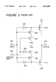
Now, operation of the circuit shown in FIG. 1 will be described with reference to FIG. 2, which illustrates waveforms on various points in the circuit shown in FIG. 1.
When an input voltage applied to the input terminal 301 is a low level, the P-channel transistor 306 is on, so that the capacitor 308 is in a condition discharged to the voltage supply level. On the other hand, the N-channel transistor 307 is off, so that the capacitor 309 is in a condition charged to the voltage supply level through the resistor 305 from the output of the inverter 303. Therefore, the output driving P-channel transistor 310 is off and the output driving N-channel transistor 311 is on, so that an voltage on the output terminal 312 is at a ground level.
When the input voltage of the input terminal 301 rises up from the low level to a high level, the output of the inverter 303 changes to the ground level, and simultaneously, the N-channel transistor 307 is brought from the off condition to the on condition, so that the capacitor 309 is discharged to the ground level, and therefore, the output driving N-channel transistor 311 is immediately turned off.
On the other hand, the P-channel transistor 306 is brought from the on condition to the off condition, and simultaneously, the output of the inverter 302 changes to the ground level. Here, since the capacitor 308 is charged by the output of the inverter 302 through the resistor 304 towards the ground level, the potential on the one end of the capacitor 308 gradually shifts to the ground level. Therefore, the output voltage on the output terminal 312 slowly rises up with a substantial rising time.
Similarly, when the input voltage of the input terminal 301 falls down from the high level to the low level, the capacitor 308 is discharged to the voltage supply level, so that the output driving P-channel transistor 310 is immediately turned off. But, the capacitor 309 is charged through the resistor 305, the potential of the capacitor 309 gradually shifts towards the voltage supply level. Accordingly, the output voltage on the output terminal 312 slowly falls down with a substantial rising time.
Referring to FIG. 3, there is shown a circuit diagram of another conventional output buffer circuit shown in FIG. 2 of Japanese Patent Application Laid-open Publication No. JP-A-2-122725.
The output buffer circuit shown in FIG. 3 is configured to be capable of selecting the rising time and the failing time between a high speed value and a low speed value by means of a control terminal 502 in accordance with an application thereof.
When a signal applied to the control terminal 502 is at a low level, both of an N-channel transistor 507 and a P-channel transistor 508 are off, so that when an output driving MOS transistor is turned on, inverters 503 and 505 having a small driving power will drive a gate of an output driving P-channel transistor 510 and an output driving N-channel transistor 511 with the small drive power, so as to turn on the output driving transistor with a slow driving speed. Therefore, an output voltage of an output terminal 512 has a slow rising time and a slow falling time.
When the signal applied to the control terminal 502 is at a high level, both of the N-channel transistor 507 and the P-channel transistor 508 are on. An N-channel transistor 506 and a P-channel transistor 509 cooperate with the inverters 503 and 505, respectively, to drive the gate of the output driving P-channel transistor 510 and the output driving N-channel transistor 511 with a large drive power, so as to turn on the output driving transistor with a high driving speed. Therefore, the output voltage of the output terminal 512 has a high rising time and a high falling time.
The above mentioned conventional output buffer circuits are so designed that, in order to make slow the rising and the falling of the output voltage on the output terminal, the capacitor means including a gate capacitance of the output driving MOS transistor is gradually charged through a resistor means, so as to turn on the output driving MOS transistor at a low speed.
Because of this reason, the time after the input voltage of the input terminal changes until the potential of the capacitor means is charged to a threshold voltage of the output driving MOS transistor, becomes long, as shown in FIG. 2, and therefore, the rising/falling propagation delay time of the output voltage becomes correspondingly long, as also shown in FIG. 2. In addition, a variation in phase of output signals become large dependently upon a manufacturing condition and a operation condition, so that it is not possible to elevate an operating frequency of the overall system.
SUMMARY OF THE INVENTION
Accordingly, it is an object of the present invention to provide an output buffer circuit which has overcome the above mentioned defect of the conventional one.
Another object of the present invention is to provide an output buffer circuit having an output voltage having a slow rising/falling time but capable of minimizing the output voltage propagation delay time.
The above and other objects of the present invention are achieved in accordance with the present invention by an output buffer circuit comprising an input terminal, an output terminal, an output driving MOS transistor having a drain electrode and a source electrode, one of which is connected to the output terminal, the output driving MOS transistor having a gate electrode for controlling an on/off of the output driving MOS transistor, a capacitor means connected to the gate of the output driving MOS transistor, a resistor means for charging the capacitor means when a potential on the input terminal is at a first signal level of turning on the output driving MOS transistor, a discharging switch means for discharging me capacitor means when the potential on the input terminal is at a second signal level of turning off the output driving MOS transistor, and a threshold voltage charging means for rapidly charging the capacitor means to a threshold voltage level of the output driving MOS transistor when the potential on the input terminal is at the first signal level of turning on the output driving MOS transistor.
The above and other objects, features and advantages of the present invention will be apparent from the following description of preferred embodiments of the invention with reference to the accompanying drawings.
BRIEF DESCRIPTION OF THE DRAWINGS
FIG. 1 is a circuit diagram illustrating one example of a conventional slew rate output buffer circuit in a CMOS technology;
FIG. 2 illustrates waveforms on various points in the circuit shown in FIG. 1;
FIG. 3 is a circuit diagram of another conventional output buffer circuit;
FIG. 4 is a circuit diagram of an embodiment of the output buffer circuit in accordance with the present invention; and
FIG. 5 illustrates waveforms on various points in the circuit shown in FIG. 4.
DESCRIPTION OF THE PREFERRED EMBODIMENT
Referring to FIG. 4, there is shown a circuit diagram of an embodiment of the output buffer circuit in accordance with the present invention.
The shown output buffer circuit in accordance with the present invention is based on the CMOS technology, and includes an output driving stage composed of a P-channel transistor 117 and an N-channel transistor 118 having their drain electrode connected in common to an output terminal 119. The P-channel transistor 117 has a source electrode connected to a voltage supply line VDD and a gate electrode connected to one end of a capacitor 108, the other end of which is connected to the voltage supply line VDD. The N-channel transistor 118 has a source electrode connected to a ground line and a gate electrode connected to one end of a capacitor 116, the other end of which is connected to the ground line. Here, each of the capacitors 108 and 116 includes a gate capacitance of the gate electrode of the MOS transistor connected with the capacitor concerned and also a wiring capacitance if any.
An input terminal 101 is connected to an input of each of inverters 102, 103 and 104, which cooperate with the input terminal 101 to control a charging/discharging timing of the capacitors 108 and 116. An output of the inverter 102 is connected through a resistor 105 to the one end of the capacitor 108 so as to charge the capacitor 108 to a ground level. A P-channel transistor 107 having its gate connected to the input terminal 101, its source connected to the voltage supply line VDD and its drain connected to the one end of the capacitor 108, acts to discharge the capacitor 108 to a voltage supply level of the voltage supply line VDD. An output of the inverter 104 is connected through a resistor 106 to the one end of the capacitor 116 so as to charge the capacitor 116 to the voltage supply level. An N-channel transistor 115 having its gate connected to the input terminal 101, its source connected to the ground line and its drain connected to the one end of the capacitor 116, acts to discharge the capacitor 116 to the ground level of the ground line.
The shown output buffer further includes a threshold voltage charging circuit I including a capacitor 110 and N-channel transistors 109 and III, and another threshold voltage charging circuit 2 including a capacitor 113 and P- channel transistors 114 and 112.
In brief, the N-channel transistor 109 has its gate connected to the input terminal 101, its source connected to one end of the capacitor 110 having its other end connected to the ground line, and its drain connected to the one end of the capacitor 108. This N-channel transistor 109 acts as a switch for connecting the capacitor 110 to the capacitor 108. The N-channel transistor 111 has its gate connected to an output of the inverter 103, its source connected to the ground line and its drain connected to the one end of the capacitor 110. This N-channel transistor 111 functions to precharge the capacitor 110 to the ground level.
The P-channel transistor 114 has its gate connected to the input terminal 101, its source connected to one end or the capacitor 113 having its other end connected to the voltage supply line VDD, and its drain connected to the one end of the capacitor 116. This P-channel transistor 114 acts as a switch for connecting the capacitor 113 to the capacitor 116. The P-channel transistor 112 has its gate connected to the output of the inverter 103, its source connected to the voltage supply line VDD and its drain connected to the one end of the capacitor 113. This P-channel transistor 112 functions to precharge the capacitor 113 to the voltage supply level.
Now, operation of the circuit shown in FIG. 4 will be described with reference to FIG. 5, which illustrates waveforms on various points in the circuit shown in FIG. 4.
When an input voltage applied to the input terminal 101 is a low level, the P-channel transistor 107 is on, and the N-channel transistor 109 is off, so that the capacitor 108 is in a condition discharged to the voltage supply level. Simultaneously, the N-channel transistor 109 is on, so that the capacitor 110 is in a condition precharged to the ground level. On the other hand, the P-channel transistor 112 and the N-channel transistor 115 are off and the P-channel transistor 114 is on, so that the capacitor 116 and the capacitor 113 are in a condition charged to the voltage supply level through the resistor 106 from the output of the inverter 104.
Therefore, the output driving P-channel transistor 117 is off and the output driving N-channel transistor 118 is on, so that an voltage on the output terminal 119 is at a ground level.
When the input voltage of the input terminal 101 rises up from the low level to a high level, the N-channel transistor 114 is brought from the on condition to the off condition, and the output of the inverter 104 changes to the ground level, and simultaneously, the N-channel transistor 115 is brought from the off condition to the on condition, so that the capacitor 116 is discharged to the ground level, and therefore, the output driving N-channel transistor 118 is immediately turned off.
On the other hand, the P-channel transistor 107 is brought from the on condition to the off condition, and simultaneously, the output of the inverter 102 changes to the ground level so as to charge the capacitor 108 towards t&e ground level through the resistor 105. At the same time, the N-channel transistor 111 is brought from the on condition to the off condition, and simultaneously, the N-channel transistor 109 is brought from the off condition to the on condition, so that the capacitor 110 is connected to the capacitor 108. Thus, electric charges precharged in the capacitor 110 is transferred to the capacitor 108, so that, as shown in FIG. 5, the potential on the capacitor 108 swiftly changes to an intermediate level which is between the voltage supply level and the ground level and which is determined by a ratio in a capacitance between the capacitor 108 and the capacitor 110. Thereafter, since the capacitor 108 and the capacitor 110 are charged through the resistor 105 from the output of the inverter 102, the potential on the one end of the capacitor 108 gradually shifts to the ground level.
Here, by designing the circuit to the effect that the above mentioned intermediate level is equal to a threshold voltage value of the output driving P-channel transistor 117, when the input voltage had risen up, the output driving P-channel transistor 117 is quickly put in a condition just before the turning-on, and thereafter, gradually becomes the on condition. Accordingly, the output voltage of the output terminal 119 takes a voltage waveform having a long rising time (slow rising-up) but a minimized rising propagation delay time.
Similarly, when the input voltage of the input terminal 101 falls down from the high level to the low level, a circuit connected to the gate of the output driving P-channel transistor 117 and a circuit connected to the gate of the output driving N-channel transistor 118 operate in a complementary manner. Namely, the capacitor 108 is discharged to the voltage supply level, so that the output driving P-channel transistor 117 is immediately turned off. On the other hand, the potential of the capacitor 116 is quickly changed to to an intermediate level which is between the voltage supply level and the ground level and which is determined by a ratio in a capacitance between the capacitor 116 and the capacitor 113, as shown in FIG. 5. Thereafter, since the capacitor 116 and the capacitor 113 are charged through the resistor 106, the potential of the capacitor 116 gradually shifts towards the voltage supply level.
Here, by designing the circuit to the effect that the above mentioned intermediate level is equal to a threshold voltage value of the output driving N-channel transistor 118, when the input voltage had fallen down, the output driving N-channel transistor 118 is quickly put in a condition just before the turning-on, and thereafter, gradually becomes the on condition. Accordingly, the output voltage of the output terminal 119 takes a voltage waveform having a long falling time (slow falling-down) but a minimized falling propagation delay time.
In the above mentioned embodiment, the P-channel transistor 117 and the N-channel transistor are used to constitute the output driving stage, but it would be apparent to persons skilled in the an that the present invention can be equally applied to an output buffer including an output driving stage composed of only a single P-channel or N-channel transistor, or an output buffer composed of field effect transistors other than MOS transistors. In addition, in order to shorten the propagation delay time in the output buffer circuit of the shown embodiment, or in order to reduce a circuit area of the output buffer circuit of the shown embodiment, the circuit can be modified by adding or deleting an inverter connected to the input terminal.
As seen from the above, the output buffer circuit so configured that a capacitor means connected to a gate of an output driving MOS transistor and including a gate capacitance of the output driving MOS transistor is gradually charged through a resistor means, so as to have a slow rising or falling time, is additionally provided, in accordance with the present invention, with a threshold voltage charging means for rapidly charging the capacitor means to a threshold voltage level of the output driving MOS transistor when the output driving MOS transistor is to be turned on. With this feature, the propagation delay time of the output voltage on the output terminal can be minimized.
In addition, when the rising or the falling is made at a slow speed in a system required to have a low noise, since the propagation delay time is minimized, the variation of phase in output signals which would be caused for variations in the manufacturing condition and in the operating condition, can be reduced. As a result, it is possible to elevate the operating frequency of the overall system.
The invention has thus been shown and described with reference to the specific embodiments. However, it should be noted that the present invention is in no way limited to the details of the illustrated structures but changes and modifications may be made within the scope of the appended claims.

Claims (4)

I claim:
1. An output buffer circuit comprising:
an input terminal;
an output terminal;
an output driving P-channel transistor having a drain electrode connected to said output terminal and a source electrode connected to a voltage supply line;
a capacitor having one end connected to a gate electrode of said output driving P-channel transistor, the other end of said capacitor being connected to said voltage supply line;
an inverter having an input connected to said input terminal and an output connected through a resistor to said one end of said capacitor;
a discharging P-channel transistor having a gate connected to said input terminal and connected in parallel to said capacitor, so that when a potential on said input terminal is brought to a low level for the purpose of turning off said output driving P-channel transistor, said discharging P-channel transistor is turned on so as to discharge said capacitor; and
a threshold voltage charging circuit connected to said one end of said capacitor and controlled by said potential on said input terminal for rapidly charging said capacitor to a threshold voltage level of said output driving P-channel transistor when the potential on said input terminal is brought to a high level for the purpose of turning on said output driving P-channel transistor.
2. An output buffer circuit claimed in claim 1 wherein said threshold voltage charging circuit includes:
a precharge capacitor having one end connected to a ground line;
a precharging N-channel transistor connected in parallel to said precharge capacitor and having a gate connected through an inverter to said input terminal so that when the potential on said input terminal is at said low level, said precharging N-channel transistor is on so as to precharge said precharge capacitor to a ground level of said ground line; and
a coupling N-channel transistor connected between said one end of said capacitor and the other end of said precharge capacitor and having a gate connected to said input terminal so that when the potential on said input terminal is brought to said high level, said coupling N-channel transistor is turned on so as to connect said one end of said capacitor to the other end of said precharge capacitor so that a potential on said one end of said capacitor is quickly brought to an intermediate level between a voltage supply level of said voltage supply line and said ground level of said ground line, said intermediate level being substantially equal to said threshold voltage level of said output driving P-channel transistor.
3. An output buffer circuit comprising:
an input terminal;
an output terminal;
an output driving N-channel transistor having a drain electrode connected to said output terminal and a source electrode connected to a ground line;
a capacitor having one end connected to a gate electrode of said output driving N-channel transistor, the other end of said capacitor being connected to said ground line;
an inverter having an input connected to said input terminal and an output connected through a resistor to said one end of said capacitor;
a discharging N-channel transistor having a gate connected to said input terminal and connected in parallel to said capacitor, so that when a potential on said input terminal is brought to a high level for the purpose of turning off said output driving N-channel transistor, said discharging N-channel transistor is turned on so as to discharge said capacitor; and
a threshold voltage charging circuit connected to said one end of said capacitor and controlled by said potential on said input terminal for rapidly charging said capacitor to a threshold voltage level of said output driving N-channel transistor when the potential on said input terminal is brought to a low level for the purpose of turning on said output driving N-channel transistor.
4. An output buffer circuit claimed in claim 3 wherein said threshold voltage charging circuit includes:
a precharge capacitor having one end connected to a voltage supply line;
a precharging P-channel transistor connected in parallel to said precharge capacitor and having a gate connected through an inverter to said input terminal so that when the potential on said input terminal is at said high level, said precharging P-channel transistor is on so as to precharge said precharge capacitor to a voltage supply level of said voltage supply line; and
a coupling P-channel transistor connected between said one end of said capacitor and the other end of said precharge capacitor and having a gate connected to said input terminal so that when the potential on said input terminal is brought to said low level, said coupling P-channel transistor is turned on so as to connect said one end of said capacitor to the other end of said precharge capacitor so that a potential on said one end of said capacitor is quickly brought to an intermediate level between a voltage supply level of said voltage supply line and said ground level of said ground line, said intermediate level being substantially equal to said threshold voltage level of said output driving N-channel transistor.
US08/536,780 1994-09-29 1995-09-29 Output buffer circuit having a minimized output voltage propagation Expired - Fee Related US5633600A (en)

Applications Claiming Priority (2)

Application Number Priority Date Filing Date Title
JP6-235151 1994-09-29
JP6235151A JP2655096B2 (en) 1994-09-29 1994-09-29 Output buffer circuit

Publications (1)

Publication Number Publication Date
US5633600A true US5633600A (en) 1997-05-27

Family

ID=16981811

Family Applications (1)

Application Number Title Priority Date Filing Date
US08/536,780 Expired - Fee Related US5633600A (en) 1994-09-29 1995-09-29 Output buffer circuit having a minimized output voltage propagation

Country Status (2)

Country Link
US (1) US5633600A (en)
JP (1) JP2655096B2 (en)

Cited By (24)

* Cited by examiner, † Cited by third party
Publication number Priority date Publication date Assignee Title
EP0902540A1 (en) * 1997-09-15 1999-03-17 Harris Corporation Constant slew rate amplifier
US5898315A (en) * 1996-05-17 1999-04-27 Cypress Semiconductor Corp. Output buffer circuit and method having improved access
US5898428A (en) * 1996-11-19 1999-04-27 Micron Display Technology Inc. High impedance transmission line tap circuit
FR2777137A1 (en) * 1998-04-06 1999-10-08 Centre Nat Rech Scient METHOD AND DEVICE FOR CONTROLLING SWITCHING OF INSULATED GRID POWER TRANSISTOR
EP0963044A3 (en) * 1998-06-02 2000-05-17 Nec Corporation Slew rate output circuit with capability of driving an output MOS field effect transistor
US6084432A (en) * 1998-03-30 2000-07-04 International Business Machines Corporation Driver circuit having reduced noise
US6111432A (en) * 1997-08-11 2000-08-29 Mhs Symmetric adapter unit for switching a logic signal
US6124734A (en) * 1998-11-20 2000-09-26 Triquint Semiconductor, Inc. High-speed push-pull output stage for logic circuits
US6195027B1 (en) 1999-04-30 2001-02-27 International Business Machines Corporation Capacitive precharging and discharging network for converting N bit input into M bit output
US6236237B1 (en) * 1998-02-27 2001-05-22 Altera Corporation Output buffer predriver with edge compensation
US6285215B1 (en) * 1999-09-02 2001-09-04 Micron Technology, Inc. Output driver having a programmable edge rate
US6433592B1 (en) * 1998-05-12 2002-08-13 Infineon Technologies Ag Method and apparatus for switching a field-effect transistor
US6653693B1 (en) * 1997-11-11 2003-11-25 Mitsubishi Denki Kabushiki Kaisha Semiconductor integrated circuit device
US20030227297A1 (en) * 2002-06-05 2003-12-11 Kabushiki Kaisha Toshiba Output buffer circuit
US20030231038A1 (en) * 2002-06-13 2003-12-18 Kenneth Koch Pulse shaping circuit and method
US6753708B2 (en) * 2002-06-13 2004-06-22 Hewlett-Packard Development Company, L.P. Driver circuit connected to pulse shaping circuitry and method of operating same
US6759880B2 (en) 2002-06-13 2004-07-06 Hewlett-Packard Development Company, L.P. Driver circuit connected to a switched capacitor and method of operating same
US20090184696A1 (en) * 2008-01-23 2009-07-23 Dimitry Patent Voltage source for gate oxide protection
US7605602B1 (en) * 2007-10-23 2009-10-20 Lattice Semiconductor Corporation Low-power output driver buffer circuit
US20100052774A1 (en) * 2006-11-21 2010-03-04 Nxp, B.V. Circuit arrangement for controlling a high side cmos transistor in a high voltage deep sub micron process
CN101807909B (en) * 2009-02-12 2012-07-25 奇景光电股份有限公司 Buffer applied to driving circuit and driving method applied to load device
CN103166623A (en) * 2011-12-09 2013-06-19 扬智科技股份有限公司 buffer
DE102016006227B3 (en) * 2016-05-19 2017-08-31 Audi Ag Electrical circuit arrangement
US11606030B1 (en) * 2020-10-15 2023-03-14 Dialog Semiconductor B.V. Driver for driving a p-type power switch

Families Citing this family (7)

* Cited by examiner, † Cited by third party
Publication number Priority date Publication date Assignee Title
JP3570596B2 (en) * 1996-12-25 2004-09-29 川崎マイクロエレクトロニクス株式会社 Output buffer circuit
KR100278608B1 (en) * 1998-01-16 2001-02-01 윤종용 Threshold Voltage Compensation Circuit
JP4526935B2 (en) * 2004-11-25 2010-08-18 パナソニック株式会社 Output buffer circuit
JP4744999B2 (en) * 2005-09-15 2011-08-10 ルネサスエレクトロニクス株式会社 Output buffer circuit
JP4989312B2 (en) * 2007-05-25 2012-08-01 旭化成エレクトロニクス株式会社 Inductive load drive circuit
JP5870712B2 (en) * 2012-01-31 2016-03-01 ローム株式会社 Electric circuit having FET, switching regulator, and electric device
US20220345128A1 (en) * 2019-12-12 2022-10-27 Panasonic Intellectual Property Management Co., Ltd. Gate drive circuit, insulated gate driver and gate drive method

Citations (6)

* Cited by examiner, † Cited by third party
Publication number Priority date Publication date Assignee Title
US4567378A (en) * 1984-06-13 1986-01-28 International Business Machines Corporation Driver circuit for controlling signal rise and fall in field effect transistor processors
JPH01194712A (en) * 1988-01-29 1989-08-04 Nec Kyushu Ltd Inverter circuit
US5017807A (en) * 1990-07-05 1991-05-21 At&T Bell Laboratories Output buffer having capacitive drive shunt for reduced noise
US5204558A (en) * 1990-09-22 1993-04-20 Mitsubishi Denki Kabushiki Kaisha Output buffer circuit and method of operation thereof with reduced power consumption
US5334889A (en) * 1990-06-20 1994-08-02 Oki Electric Industry, Co., Ltd. CMOS output buffer circuit with less noise
US5471150A (en) * 1992-12-30 1995-11-28 Samsung Electronics Co., Ltd. Buffer with high and low speed input buffers

Family Cites Families (1)

* Cited by examiner, † Cited by third party
Publication number Priority date Publication date Assignee Title
JPS6422109A (en) * 1987-07-16 1989-01-25 Nec Corp Semiconductor device

Patent Citations (6)

* Cited by examiner, † Cited by third party
Publication number Priority date Publication date Assignee Title
US4567378A (en) * 1984-06-13 1986-01-28 International Business Machines Corporation Driver circuit for controlling signal rise and fall in field effect transistor processors
JPH01194712A (en) * 1988-01-29 1989-08-04 Nec Kyushu Ltd Inverter circuit
US5334889A (en) * 1990-06-20 1994-08-02 Oki Electric Industry, Co., Ltd. CMOS output buffer circuit with less noise
US5017807A (en) * 1990-07-05 1991-05-21 At&T Bell Laboratories Output buffer having capacitive drive shunt for reduced noise
US5204558A (en) * 1990-09-22 1993-04-20 Mitsubishi Denki Kabushiki Kaisha Output buffer circuit and method of operation thereof with reduced power consumption
US5471150A (en) * 1992-12-30 1995-11-28 Samsung Electronics Co., Ltd. Buffer with high and low speed input buffers

Cited By (34)

* Cited by examiner, † Cited by third party
Publication number Priority date Publication date Assignee Title
US5898315A (en) * 1996-05-17 1999-04-27 Cypress Semiconductor Corp. Output buffer circuit and method having improved access
US6107999A (en) * 1996-11-19 2000-08-22 Micron Technology, Inc. High impedance transmission line tap circuit
US5898428A (en) * 1996-11-19 1999-04-27 Micron Display Technology Inc. High impedance transmission line tap circuit
US6111432A (en) * 1997-08-11 2000-08-29 Mhs Symmetric adapter unit for switching a logic signal
EP0902540A1 (en) * 1997-09-15 1999-03-17 Harris Corporation Constant slew rate amplifier
US6040707A (en) * 1997-09-15 2000-03-21 Intersil Corporation Constant slew rate amplifier
US6653693B1 (en) * 1997-11-11 2003-11-25 Mitsubishi Denki Kabushiki Kaisha Semiconductor integrated circuit device
US6236237B1 (en) * 1998-02-27 2001-05-22 Altera Corporation Output buffer predriver with edge compensation
US6084432A (en) * 1998-03-30 2000-07-04 International Business Machines Corporation Driver circuit having reduced noise
WO1999052212A1 (en) * 1998-04-06 1999-10-14 Centre National De La Recherche Scientifique (Cnrs) Method and device for controlling an insulated grid power transistor switching
FR2777137A1 (en) * 1998-04-06 1999-10-08 Centre Nat Rech Scient METHOD AND DEVICE FOR CONTROLLING SWITCHING OF INSULATED GRID POWER TRANSISTOR
US6433592B1 (en) * 1998-05-12 2002-08-13 Infineon Technologies Ag Method and apparatus for switching a field-effect transistor
EP0963044A3 (en) * 1998-06-02 2000-05-17 Nec Corporation Slew rate output circuit with capability of driving an output MOS field effect transistor
US6222403B1 (en) 1998-06-02 2001-04-24 Nec Corporation Slew rate output circuit with an improved driving capability of driving an output MOS field effect transistor
US6124734A (en) * 1998-11-20 2000-09-26 Triquint Semiconductor, Inc. High-speed push-pull output stage for logic circuits
US6195027B1 (en) 1999-04-30 2001-02-27 International Business Machines Corporation Capacitive precharging and discharging network for converting N bit input into M bit output
US6285215B1 (en) * 1999-09-02 2001-09-04 Micron Technology, Inc. Output driver having a programmable edge rate
US20030227297A1 (en) * 2002-06-05 2003-12-11 Kabushiki Kaisha Toshiba Output buffer circuit
US6798247B2 (en) * 2002-06-05 2004-09-28 Kabushiki Kaisha Toshiba Output buffer circuit
US6753708B2 (en) * 2002-06-13 2004-06-22 Hewlett-Packard Development Company, L.P. Driver circuit connected to pulse shaping circuitry and method of operating same
US6759880B2 (en) 2002-06-13 2004-07-06 Hewlett-Packard Development Company, L.P. Driver circuit connected to a switched capacitor and method of operating same
US20040160261A1 (en) * 2002-06-13 2004-08-19 Kenneth Koch Driver circuit connected to pulse shaping circuitry
US20040169973A1 (en) * 2002-06-13 2004-09-02 Kenneth Koch Driver circuit connected to a switched capacitor and method of operating same
US20030231038A1 (en) * 2002-06-13 2003-12-18 Kenneth Koch Pulse shaping circuit and method
US7239185B2 (en) 2002-06-13 2007-07-03 Hewlett-Packard Development Company, L.P. Driver circuit connected to pulse shaping circuitry
US8004318B2 (en) * 2006-11-21 2011-08-23 Nxp B.V. Circuit arrangement for controlling a high side CMOS transistor in a high voltage deep sub micron process
US20100052774A1 (en) * 2006-11-21 2010-03-04 Nxp, B.V. Circuit arrangement for controlling a high side cmos transistor in a high voltage deep sub micron process
US7605602B1 (en) * 2007-10-23 2009-10-20 Lattice Semiconductor Corporation Low-power output driver buffer circuit
US7652524B2 (en) * 2008-01-23 2010-01-26 Advanced Micro Devices, Inc. Voltage source for gate oxide protection
US20090184696A1 (en) * 2008-01-23 2009-07-23 Dimitry Patent Voltage source for gate oxide protection
CN101807909B (en) * 2009-02-12 2012-07-25 奇景光电股份有限公司 Buffer applied to driving circuit and driving method applied to load device
CN103166623A (en) * 2011-12-09 2013-06-19 扬智科技股份有限公司 buffer
DE102016006227B3 (en) * 2016-05-19 2017-08-31 Audi Ag Electrical circuit arrangement
US11606030B1 (en) * 2020-10-15 2023-03-14 Dialog Semiconductor B.V. Driver for driving a p-type power switch

Also Published As

Publication number Publication date
JPH0897700A (en) 1996-04-12
JP2655096B2 (en) 1997-09-17

Similar Documents

Publication Publication Date Title
US5633600A (en) Output buffer circuit having a minimized output voltage propagation
US4779013A (en) Slew-rate limited output driver having reduced switching noise
JPS63112893A (en) Semiconductor integrated circuit
JPS5937895B2 (en) delay circuit
US5151620A (en) CMOS input buffer with low power consumption
JPH0158896B2 (en)
US4638182A (en) High-level CMOS driver circuit
JP2915625B2 (en) Data output circuit
JPH1022796A (en) Timing circuit
US7816969B2 (en) Level shifter circuit
US6982577B2 (en) Power-on reset circuit
US4468576A (en) Inverter circuit having transistors operable in a shallow saturation region for avoiding fluctuation of electrical characteristics
JPH06152374A (en) Output circuit
US5880630A (en) Gain stage and offset voltage elimination method
JP3190086B2 (en) Boost circuit
US4611134A (en) Bootstrap driving circuit
US4902919A (en) Inverting latching bootstrap driver with Vdd *2 booting
JP2690624B2 (en) Buffer circuit
US5247214A (en) Bi-cmos out buffer circuit for cmos logic
JP3899110B2 (en) Wave shaping circuit
JPS5842558B2 (en) address buffer circuit
JPH03179814A (en) Level shift circuit
JPH0332113A (en) Semiconductor integrated circuit device
JP2586196B2 (en) Output circuit
US5495099A (en) High speed super push-pull logic (SPL) circuit using bipolar technology

Legal Events

Date Code Title Description
AS Assignment

Owner name: NEC CORPORATION, JAPAN

Free format text: ASSIGNMENT OF ASSIGNORS INTEREST;ASSIGNOR:OHNISHI, YASUHIRO;REEL/FRAME:007701/0273

Effective date: 19950929

FEPP Fee payment procedure

Free format text: PAYOR NUMBER ASSIGNED (ORIGINAL EVENT CODE: ASPN); ENTITY STATUS OF PATENT OWNER: LARGE ENTITY

FPAY Fee payment

Year of fee payment: 4

FPAY Fee payment

Year of fee payment: 8

REMI Maintenance fee reminder mailed
LAPS Lapse for failure to pay maintenance fees

Free format text: PATENT EXPIRED FOR FAILURE TO PAY MAINTENANCE FEES (ORIGINAL EVENT CODE: EXP.); ENTITY STATUS OF PATENT OWNER: LARGE ENTITY

STCH Information on status: patent discontinuation

Free format text: PATENT EXPIRED DUE TO NONPAYMENT OF MAINTENANCE FEES UNDER 37 CFR 1.362

FP Lapsed due to failure to pay maintenance fee

Effective date: 20090527