US5600159A - Solid state image sensing device having facilitated output signal correction - Google Patents
Solid state image sensing device having facilitated output signal correction Download PDFInfo
- Publication number
- US5600159A US5600159A US08/358,628 US35862894A US5600159A US 5600159 A US5600159 A US 5600159A US 35862894 A US35862894 A US 35862894A US 5600159 A US5600159 A US 5600159A
- Authority
- US
- United States
- Prior art keywords
- charge
- transfer path
- charge transfer
- signal charges
- transferring
- Prior art date
- Legal status (The legal status is an assumption and is not a legal conclusion. Google has not performed a legal analysis and makes no representation as to the accuracy of the status listed.)
- Expired - Lifetime
Links
- 239000007787 solid Substances 0.000 title claims abstract description 36
- 230000002463 transducing effect Effects 0.000 claims abstract description 7
- 238000007599 discharging Methods 0.000 claims description 19
- 238000000034 method Methods 0.000 claims description 13
- 239000004065 semiconductor Substances 0.000 claims description 12
- 239000000758 substrate Substances 0.000 claims description 12
- 238000009792 diffusion process Methods 0.000 claims description 6
- 239000012535 impurity Substances 0.000 claims description 6
- 239000000872 buffer Substances 0.000 description 10
- 230000007547 defect Effects 0.000 description 4
- 229910021420 polycrystalline silicon Inorganic materials 0.000 description 3
- 229920005591 polysilicon Polymers 0.000 description 3
- 230000002159 abnormal effect Effects 0.000 description 2
- 238000001444 catalytic combustion detection Methods 0.000 description 2
- 238000010586 diagram Methods 0.000 description 2
- 238000006243 chemical reaction Methods 0.000 description 1
- 230000001678 irradiating effect Effects 0.000 description 1
Images


Classifications
-
- H—ELECTRICITY
- H01—ELECTRIC ELEMENTS
- H01L—SEMICONDUCTOR DEVICES NOT COVERED BY CLASS H10
- H01L27/00—Devices consisting of a plurality of semiconductor or other solid-state components formed in or on a common substrate
- H01L27/14—Devices consisting of a plurality of semiconductor or other solid-state components formed in or on a common substrate including semiconductor components sensitive to infrared radiation, light, electromagnetic radiation of shorter wavelength or corpuscular radiation and specially adapted either for the conversion of the energy of such radiation into electrical energy or for the control of electrical energy by such radiation
- H01L27/144—Devices controlled by radiation
- H01L27/146—Imager structures
- H01L27/148—Charge coupled imagers
-
- H—ELECTRICITY
- H04—ELECTRIC COMMUNICATION TECHNIQUE
- H04N—PICTORIAL COMMUNICATION, e.g. TELEVISION
- H04N25/00—Circuitry of solid-state image sensors [SSIS]; Control thereof
- H04N25/70—SSIS architectures; Circuits associated therewith
- H04N25/71—Charge-coupled device [CCD] sensors; Charge-transfer registers specially adapted for CCD sensors
- H04N25/713—Transfer or readout registers; Split readout registers or multiple readout registers
-
- H—ELECTRICITY
- H04—ELECTRIC COMMUNICATION TECHNIQUE
- H04N—PICTORIAL COMMUNICATION, e.g. TELEVISION
- H04N25/00—Circuitry of solid-state image sensors [SSIS]; Control thereof
- H04N25/60—Noise processing, e.g. detecting, correcting, reducing or removing noise
- H04N25/62—Detection or reduction of noise due to excess charges produced by the exposure, e.g. smear, blooming, ghost image, crosstalk or leakage between pixels
- H04N25/625—Detection or reduction of noise due to excess charges produced by the exposure, e.g. smear, blooming, ghost image, crosstalk or leakage between pixels for the control of smear
Definitions
- the present invention relates to a solid state image sensing device, and more specifically to a solid state image sensing device of multiline CCD (charge coupled device) register structure.
- CCD charge coupled device
- a multiline CCD image sensor has been known as an image sensor suitable for the image reading devices.
- An example of this image sensor is composed of a photoelectric transfer elements arranged in a straight line (each element of which corresponds to one pixel), a shift register, two-stage charge transfer sections (registers) composed of a plurality of CCDs, and an output section (buffer).
- the signal charges generated by the photoelectric transfer elements are transferred to the charge transfer section via a shift gate at a predetermined timing and further transferred to the output section at another predetermined timing for conversion into voltage signals.
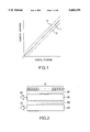
- FIG. 1 shows the relationship between the signal charge generated by the photoelectric transfer section and output charge outputted after transferred between the two registers, in which 1 denotes the normal charge; 2 denotes the abnormal charge excluding the remaining charge, and 3 denotes the abnormal charge including the remaining charge.
- 1 denotes the normal charge
- 2 denotes the abnormal charge excluding the remaining charge
- 3 denotes the abnormal charge including the remaining charge.
- the present invention provides a solid state image sensing device, comprising: photoelectric transferring means composed of a plurality of photoelectric transfer elements arranged in a straight line, for transducing incident light into signal charges; at least first and second charge transfer paths arranged in parallel to the photoelectric transfer elements and each having a plurality of charge coupled devices, for transferring the signal charges; charge transferring means for transferring the signal charges from said photoelectric transferring means to said first charge transfer path at a first timing and for transferring the signal charges transferred to said first charge transfer path to said second charge transfer path at a second timing; and charge supplying means for applying a bias charge to the signal charges to be transferred from said first charge transfer path to said second charge transfer path.
- the charge supplying means comprises a charge input drain region for transducing incident light into the bias charge and a charge input electrode for applying the bias charge to the signal charges to be transferred, both the charge input drain region and electrode being formed on a semiconductor substrate.
- the image sensing device further comprises discharging means for discharging the bias charge from said first and second charge transfer paths, respectively.
- the present invention provides a method of transferring charges in a solid state image sensing device having at least first and second charge transfer paths for transferring signal charges and charge transferring means for transferring the signal charges between the first and second charge transfer paths, which comprises the steps of: supplying a bias charge to the first charge transfer path; transferring the bias charge from the first charge transfer path to the second charge transfer path; supplying the signal charges to the first charge transfer path; transferring the signal charges from the first charge transfer path to the second charge transfer path; and outputting the signal charges and the bias charge both transferred to the second charge transfer path.
- the method of transferring charges further comprises the step of discharging the bias charge from the second charge transfer path. Further, it is preferable that before the signal charges are transferred to the second charge transfer path, the bias charge is outputted from the second charge transfer path; and the outputted bias charge is subtracted from a charge composed of the signal charge and the bias charge both outputted from the second charge transfer path, to obtain a signal output charge.
- FIG. 1 is a characteristic diagram showing the relationship between the signal charge and the output charge output after transfer between the registers in the prior art image sensing device
- FIG. 2 is a plan view showing a linear image sensor of multiline CCD structure
- FIG. 3 is a partial plan view showing a first embodiment of the solid state image sensing device according to the present invention.
- FIG. 4 is a cross-sectional view taken along a line C--C' in FIG. 3;
- FIG. 5 is a cross-sectional view taken along a line A--A' in FIG. 3;
- FIG. 6 is a cross-sectional view taken along a line B--B' in FIG. 3;
- FIGS. 7 to 11 are partial plan views for assistance in explaining the operation of a first embodiment of the solid state image sensing device according to the present invention.
- FIG. 12 is a charge transfer timing chart of the first embodiment of the solid state image sensing device
- FIG. 13 is a characteristic diagram showing the relationship between the signal charge and the output charge output after transfer between the registers in the image sensing device according to the present invention.
- FIGS. 14 to 17 are partial plan views for assistance in explaining the operation of a second embodiment of the solid state image sensing device according to the present invention.
- FIG. 18 is a charge transfer timing chart of the second embodiment of the solid state image sensing device.
- FIGS. 19 to 24 are partial plan views for assistance in explaining the operation of a third embodiment of the solid state image sensing device according to the present invention.
- FIG. 25 is a charge transfer timing chart of the third embodiment of the solid state image sensing device.
- FIGS. 26 to 31 are partial plan views for assistance in explaining the apparition of a fourth embodiment of the solid state image sensing device according to the present invention.
- FIG. 32 is a charge transfer timing chart of the fourth embodiment of the solid state image sensing device.
- FIG. 33 is a cross-sectional view taken along a line A--A' in FIG. 26.
- FIG. 2 shows an image sensor of multiline CCD register structure according to the present invention, which is formed on a semiconductor substrate.
- the image sensor is composed of a photoelectric transfer element line 10 (each element of which corresponds to one pixel), a shift register 20, two stage charge transfer sections (registers) 30 and 60 each composed of a plurality of CCDs, a transfer gate 50, and two output sections (buffers) 40 and 70.
- FIG. 3 is an enlarged plane view showing a part of the image sensor shown in FIG. 2.
- the shift gate 20 and the transfer gate 50 are connected to dedicated drive pulse lines SH (SH1 and SH2) and TG, respectively.
- drive pulse lines P1 and P2 are connected alternately to the arranged transfer electrodes of the CCD registers 30 and 60, respectively.
- the drive pulse lines SH1 and SH2 are connected alternately to the arranged electrodes of the shift gate 20. That is, the respective electrodes of the shift gate 20 are arranged and connected alternately to either of the drive pulse lines SH1 or SH2. Further, since the shift gates 20 shown in figures other than FIG. 3 are of the same structure as that shown in FIG. 3, the reference symbols SH1 and SH2 are omitted herein in the other figures.
- each photoelectric transfer element 10 is formed in an impurity diffusion region formed in a surface of a semiconductor substrate 100.
- the shift gate 20, the transfer gate 50, and the CCD registers 30 and 60 are composed of electrodes (e.g., formed of polysilicon) formed on the semiconductor substrate 100, respectively.
- an input section is composed of a charge input electrode 110 and a charge input drain region 120 both formed in the CCD register 30 to inject fat zero charge bias charge) to the CCD register S0.
- the charge input electrode 110 is an electrode formed of polysilicon on the semiconductor substrate 100.
- the charge input electrode 110 is connected to a drive pulse line IG, and the charge input drain region 120 is connected to a drive pulse line 18.
- the input section 120 is formed by an impurity diffusion region formed in the surface of the semiconductor substrate 100, which constitutes a kind of photoelectric transfer section for obtaining the fat zero charge on the basis of light incident thereupon.
- the drive pulse line IG connected to the input section 110 is turned on to inject fat zero charges 30a from the input section 110 to the CCD register 30 (see FIG. 3). Further, at time t2, the drive pulse line TG connected to the transfer gate 50 is turned on to transfer the fat zero charges 30a from the CCD register 30 to the CCD register 60 (see FIG. 7).
- the fat zero charge 30a is transferred to the CCD register 60 by leaving a remaining charge 30b at the CCD register 30 (as a charge 60a excluding a remaining fat zero charge 30b).
- the drive pulse line SH1 connected to the shift register 20 is turned on to transfer signal charges 30c from the photoelectric transfer elements 10 to the CCD register 30 alternately (see FIG.
- the drive pulse line TG connected to the transfer gate 50 is turned on to transfer the signal charges 30c together with the remaining fat zero charge 30b from the CCD register 30 to the CCD register 60 (see FIG. 9), because the remaining fat zero charge 30b still remains at the first CCD register 30.
- the drive pulse line SH2 connected to the shift register 20 is turned on to transfer signal charges 30d from the remaining photoelectric transfer elements 10 to the CCD register 30 alternately (see FIG. 10).
- the signal charges 30d are shifted within the CCD register 30 to join the remaining fat zero charge 30b on the basis of two-phase pulses P1 and P2 (see FIG. 11).
- the joined charges are outputted through an output buffer (not shown).
- the signal charges 30c are shifted within the CCD register 60 to join the signal charges 30c with the fat zero charge 30a or 60a on the basis of the two-phase pulses P1 and P2 (see FIG. 11).
- the joined charges are outputted through an output buffer (not shown).
- the signal charges transferred from the photoelectric transfer elements 10 alternately are joined with the fat zero charges and the remaining charges, it is possible to obtain the signal charge (30d+30b) obtained by adding the normal signal charge 30d and the remaining fat zero charge 30b, the signal charge (30c+30a) obtained by adding the signal charge 30c and the normal fat zero charge 30a, and the signal charge (30d+60a) obtained by adding the signal charge 30d and the small fat zero charge 60a, in addition to the normal signal charges 30c and 30d.
- FIG. 13 shows the relationship between the magnitude of the signal charge and the magnitude of the output charge obtained after transfer between the two CCD registers 30 and 60 at this time; that is, FIG. 13 shows the characteristics showing the dependency of the magnitude of the output charge of the image sensing device upon the magnitude of the signal charge obtained by the photoelectric transfer elements in this embodiment.
- the ordinate indicate the output charge magnitude
- the abscissa indicates the signal charge magnitude.
- a second embodiment of the present invention will be described herein below with reference to FIGS. 14 to 18. Further, in the respective embodiments described later, the assumption is made that there exists a defect in the charge transfer path between the CCD 31 (see FIG. 7) of the CCD register 30 and the CCD 61 (see FIG. 7) of the CCD register 60, in the same way as with the case of the first embodiment.
- the feature of this second embodiment is that the signal charge is joined with the fat zero charge, and after that the joined charges are transferred from the CCD register 30 to the CCD register 60.
- the drive pulse line IG connected to the input section 110 and the drive pulse line SH1 connected to the shift register 20 are both turned on to inject the fat zero charges 30a from the input section 110 to the CCD register 30.
- the signal charges 30c of the photoelectric transfer elements 10 are transferred to the CCD register 30 alternately (see FIG. 14).
- the drive pulse line TG connected to the transfer gate 50 is turned on to transfer the signal charges 30c and the fat zero charge 30a from the CCD register 30 to the CCD register 60 (see FIG. 15).
- the fat zero charge shown at the middle in FIG. 15 is transferred by leaving the remaining fat zero charge 30b in the CCD register 30.
- the drive pulse line SH2 connected to the shift register 20 is turned on to transfer the signal charges 30d from the photoelectric transfer elements 10 to the CCD register 30 alternately (see FIG. 16).
- the signal charges 30d are shifted within the CCD register 30 on the basis of the two-phase pulses P1 and P2 to join the signal charges 30d with the remaining fat zero charge 30b (see FIG. 17), and then outputted through the output buffer.
- the signal charges 30c are shifted within the CCD register 60 on the basis of the two-phase pulses P1 and P2 to join the signal charges 30c with the fat zero charge 30a (see FIG. 17), and then outputted through the output buffer.
- the signal charges transferred from the photoelectric transfer elements 10 alternately are joined with the fat zero charges and the remaining charges, it is possible to obtain the signal charge (30d+30b) obtained by adding the normal signal charge 30d and the remaining fat zero charge 30b, the signal charge (30c+30a) obtained by adding the signal charge 30c and the normal fat zero charge 30a, and the signal charge (30c+60a) obtained by adding the signal charge 30c and the small fat zero charge 60a, in addition to the normal signal charges 30c and 30d.
- the dependency of the magnitude of the output charge upon the magnitude of the signal charge is the same as shown in FIG. 13. Since the non-linear characteristics are maintained when the signal charge magnitude is small, although the offset rate changes according to the presence or absence of the remaining charge, it is possible to correct the signals easily along the linear characteristics.
- the signal charges are transferred once between the CCD registers.
- the signal charges are transferred several times, it is necessary to retrain the remaining charges the same electrode while the signal charges are transferred between the CCD registers. This case will be described hereinbelow.
- a third embodiment corresponding to this case will be described hereinbelow with reference to FIGS. 19 to 25.
- the feature of this third embodiment is to provide charge discharging sections 130 and 140 for discharging the charges of the CCD register 60.
- the charge discharging section 130 is composed of polysilicon electrodes formed on the semiconductor substrate 100 and connected to a drive pulse line OFG.
- the charge discharging section 140 is composed of impurity diffusion regions formed in the surface of the semiconductor substrate 100 and connected to a drive pulse line OFD.
- the drive pulse line IG connected to the input section 110 is turned on to inject the fat zero charges 30a from the input section 110 to the CCD register 30 (see FIG. 19).
- the drive pulse line TG connected to the transfer gate 50 is turned on to transfer the fat zero charges 30a from the CCD register 30 to the CCD register 60 (see FIG. 20).
- the fat zero charge at the middle of the CCD register 30 is transferred to the CCD register 60 by leaving the remaining fat zero charge 30b thereat.
- the drive pulse line OFG connected to the charge discharging section 130 is turned on to transfer the fat zero charges 30a of the CCD register 60 to the charge discharging section 140 so that the fat zero charges 30a ere removed from the register transfer path (see FIG. 21).
- the drive pulse line SH1 connected to the shift register 2 is turned on to transfer the signal charges of the photoelectric transfer elements 10 to the CCD register 30 alternately (see FIG. 22).
- the signal charges 30c are transferred from the CCD register 30 to the CCD register 60 together with the remaining fat zero charge (see FIG. 23).
- the remaining fat zero charge 30b still remains at the CCD register 30.
- the drive pulse line SH2 connected to the shift register 20 is turned on to transfer the signal charges from the remaining photoelectric transfer elements 10 to the CCD register 30 alternately.
- the signal charges 30d are shifted within the CCD register 30 on the basis of the two-phase pulses P1 and P2 to join the signal charge 30d with the remaining fat zero charge 30b (see FIG. 24), and the joined charges are outputted through an output buffer.
- the signal charges 30c are shifted within the CCD register 60 on the basis of the two-phase pulses P1 and P2 and outputted through an output buffer.
- the charge added to the signal charge is only the remaining fat zero charge, so that it is possible to reduce the magnitude of the charge to be transferred between the CCD registers 30 and 60. Further, since the fat zero charge is not added to the signal charge, the signal charge is not subjected to the influence of noise included in the fat zero charge. Further, instead of the charge discharging section, it is also possible to provide another set of the transfer gate and the CCD register in the vicinity of the CCD register 60 to transfer the fat zero charge to the additional CCD register.
- FIG. 33 is a cross-sectional view showing the semiconductor substrate 100 taken along the line A--A' shown in FIG. 26.
- the charge discharging sections 150 and 160 are additionally formed to discharge the charges in the CCD registers 30 and 60, respectively.
- These charge discharging sections 150 and 160 are formed by N-type impurity diffusion regions buried just under the register electrodes 30 and 60, respectively, and connected to drive pulse lines D1 and D2, respectively.
- the drive pulse line IG connected to the input section 110 is turned on to inject the fat zero charges 30a from the input section 110 to the CCD register 30 (see FIG. 26).
- the drive pulse line TG connected to the transfer gate 50 is turned on to transfer the fat zero charges 30a from the CCD register 30 to the CCD register 60 (see FIG. 27).
- the fat zero charge at the middle of the CCD register 30 is transferred to the CCD register 60 by leaving the remaining fat zero charge 30b at the CCD register 30.
- the drive pulse line SH1 connected to the shift register 20 is turned on to transfer the signal charges of the photoelectric transfer elements 10 to the CCD register 30 alternately (see FIG. 28).
- the drive pulse line D2 connected to the charge discharging section 160 is turned on to discharge the fat zero charges 30a of the CCD register 60.
- the signal charges 30c are transferred from the CCD register 30 to the CCD register 60 together with the remaining charge (see FIG. 29). In this case, the remaining fat zero charge 30b remains at the CCD register 30.
- the drive pulse line D1 connected to the charge discharging section 150 is turned on to discharge the remaining fat zero charge 30b at the CCD register 30.
- the drive pulse line SH2 connected to the shift register 20 is turned on to transfer the signal charges 30d of the remaining photoelectric transfer elements 10 to the CCD register 30 alternately (see FIG. 30).
- the signal charge 30d are shifted within the CCD register 30 on the basis of the two-phase pulses P1 and P2 (see FIG. 31), and then outputted through an output buffer.
- the signal charges 30c are shifted within the CCD register 60 on the basis of the two-phase pulses P1 and P2, and then outputted through an output buffer.
- the fat zero charges are injected to the CCD register and since the remaining signal charges can be kept constant, after the transfer between the two CCD registers, irrespective of the magnitude of the signal charges, it is possible to easily correct the signals even if remaining signal charges are generated. Further, when the remaining charges are discharged, it is possible to eliminate the remaining signal charges.
Landscapes
- Engineering & Computer Science (AREA)
- Multimedia (AREA)
- Signal Processing (AREA)
- Physics & Mathematics (AREA)
- Power Engineering (AREA)
- Electromagnetism (AREA)
- Condensed Matter Physics & Semiconductors (AREA)
- General Physics & Mathematics (AREA)
- Computer Hardware Design (AREA)
- Microelectronics & Electronic Packaging (AREA)
- Solid State Image Pick-Up Elements (AREA)
- Transforming Light Signals Into Electric Signals (AREA)
Applications Claiming Priority (2)
| Application Number | Priority Date | Filing Date | Title |
|---|---|---|---|
| JP5-342217 | 1993-12-15 | ||
| JP34221793A JP3155877B2 (ja) | 1993-12-15 | 1993-12-15 | 固体撮像装置及びその電荷転送方法 |
Publications (1)
| Publication Number | Publication Date |
|---|---|
| US5600159A true US5600159A (en) | 1997-02-04 |
Family
ID=18352029
Family Applications (1)
| Application Number | Title | Priority Date | Filing Date |
|---|---|---|---|
| US08/358,628 Expired - Lifetime US5600159A (en) | 1993-12-15 | 1994-12-14 | Solid state image sensing device having facilitated output signal correction |
Country Status (6)
| Country | Link |
|---|---|
| US (1) | US5600159A (zh) |
| EP (1) | EP0659014B1 (zh) |
| JP (1) | JP3155877B2 (zh) |
| KR (1) | KR100196817B1 (zh) |
| CN (1) | CN1035705C (zh) |
| DE (1) | DE69427272T2 (zh) |
Cited By (1)
| Publication number | Priority date | Publication date | Assignee | Title |
|---|---|---|---|---|
| US6107655A (en) * | 1997-08-15 | 2000-08-22 | Eastman Kodak Company | Active pixel image sensor with shared amplifier read-out |
Families Citing this family (3)
| Publication number | Priority date | Publication date | Assignee | Title |
|---|---|---|---|---|
| JP4862473B2 (ja) * | 2005-10-28 | 2012-01-25 | ソニー株式会社 | 固体撮像装置、固体撮像装置の駆動方法および撮像装置 |
| JP5134427B2 (ja) | 2008-04-30 | 2013-01-30 | 浜松ホトニクス株式会社 | 固体撮像装置 |
| JP5328224B2 (ja) * | 2008-05-01 | 2013-10-30 | キヤノン株式会社 | 固体撮像装置 |
Citations (8)
| Publication number | Priority date | Publication date | Assignee | Title |
|---|---|---|---|---|
| EP0033129A1 (en) * | 1980-01-25 | 1981-08-05 | Kabushiki Kaisha Toshiba | Charge transfer apparatus |
| US4443886A (en) * | 1980-11-07 | 1984-04-17 | Sony Corporation | Charge transfer device imager with bias charge |
| US4541068A (en) * | 1983-05-23 | 1985-09-10 | Rca Corporation | Reducing noise in introducing bias charge into charge transfer devices |
| US4551757A (en) * | 1981-10-22 | 1985-11-05 | Matsushita Electric Industrial Co., Ltd. | Method for driving solid-state image sensor |
| US4912560A (en) * | 1988-01-29 | 1990-03-27 | Kabushiki Kaisha Toshiba | Solid state image sensing device |
| EP0398228A2 (en) * | 1989-05-15 | 1990-11-22 | Sanyo Electric Co., Ltd. | Solid image pickup apparatus for eliminating smear |
| EP0444696A2 (en) * | 1990-03-02 | 1991-09-04 | Sony Corporation | Solid state image sensor |
| EP0553869A2 (en) * | 1992-01-31 | 1993-08-04 | Kabushiki Kaisha Toshiba | Method for transferring charge, charge transfer device and solid state image sensing device using the same |
-
1993
- 1993-12-15 JP JP34221793A patent/JP3155877B2/ja not_active Expired - Fee Related
-
1994
- 1994-12-09 KR KR1019940033430A patent/KR100196817B1/ko not_active IP Right Cessation
- 1994-12-14 CN CN94120782A patent/CN1035705C/zh not_active Expired - Fee Related
- 1994-12-14 US US08/358,628 patent/US5600159A/en not_active Expired - Lifetime
- 1994-12-15 DE DE69427272T patent/DE69427272T2/de not_active Expired - Fee Related
- 1994-12-15 EP EP94119832A patent/EP0659014B1/en not_active Expired - Lifetime
Patent Citations (8)
| Publication number | Priority date | Publication date | Assignee | Title |
|---|---|---|---|---|
| EP0033129A1 (en) * | 1980-01-25 | 1981-08-05 | Kabushiki Kaisha Toshiba | Charge transfer apparatus |
| US4443886A (en) * | 1980-11-07 | 1984-04-17 | Sony Corporation | Charge transfer device imager with bias charge |
| US4551757A (en) * | 1981-10-22 | 1985-11-05 | Matsushita Electric Industrial Co., Ltd. | Method for driving solid-state image sensor |
| US4541068A (en) * | 1983-05-23 | 1985-09-10 | Rca Corporation | Reducing noise in introducing bias charge into charge transfer devices |
| US4912560A (en) * | 1988-01-29 | 1990-03-27 | Kabushiki Kaisha Toshiba | Solid state image sensing device |
| EP0398228A2 (en) * | 1989-05-15 | 1990-11-22 | Sanyo Electric Co., Ltd. | Solid image pickup apparatus for eliminating smear |
| EP0444696A2 (en) * | 1990-03-02 | 1991-09-04 | Sony Corporation | Solid state image sensor |
| EP0553869A2 (en) * | 1992-01-31 | 1993-08-04 | Kabushiki Kaisha Toshiba | Method for transferring charge, charge transfer device and solid state image sensing device using the same |
Cited By (2)
| Publication number | Priority date | Publication date | Assignee | Title |
|---|---|---|---|---|
| US6107655A (en) * | 1997-08-15 | 2000-08-22 | Eastman Kodak Company | Active pixel image sensor with shared amplifier read-out |
| US6352869B1 (en) | 1997-08-15 | 2002-03-05 | Eastman Kodak Company | Active pixel image sensor with shared amplifier read-out |
Also Published As
| Publication number | Publication date |
|---|---|
| CN1118522A (zh) | 1996-03-13 |
| CN1035705C (zh) | 1997-08-20 |
| JP3155877B2 (ja) | 2001-04-16 |
| EP0659014B1 (en) | 2001-05-23 |
| JPH07169935A (ja) | 1995-07-04 |
| DE69427272T2 (de) | 2001-10-25 |
| KR950021709A (ko) | 1995-07-26 |
| DE69427272D1 (de) | 2001-06-28 |
| EP0659014A1 (en) | 1995-06-21 |
| KR100196817B1 (ko) | 1999-06-15 |
Similar Documents
| Publication | Publication Date | Title |
|---|---|---|
| US20170034462A1 (en) | Solid-state imaging element having image signal overflow path | |
| KR100283351B1 (ko) | 반도체집적회로 | |
| US5493423A (en) | Resettable pixel amplifier for an image sensor array | |
| JPS60214173A (ja) | イメージセンサ用オフセット補正装置 | |
| US4366503A (en) | Solid state image pick-up device and its charge transfer method | |
| US4597013A (en) | Solid state image sensor | |
| GB2071959A (en) | Signal pick-up circuit arrangements | |
| US7196303B2 (en) | CCD image sensor | |
| US5600159A (en) | Solid state image sensing device having facilitated output signal correction | |
| US6473125B1 (en) | Solid-state imaging device with shutter operation in sync with signal charge reset and method of driving same | |
| US4777519A (en) | Charge transfer device | |
| US4603343A (en) | Solid state image sensor applied with differing read-out gate voltages | |
| US6515318B2 (en) | Charge transfer device | |
| JPH05218105A (ja) | 電荷転送素子 | |
| US5973736A (en) | Color linear sensor | |
| US4300062A (en) | Offset compensation circuit for charge-coupled devices | |
| JP2973650B2 (ja) | 電荷転送装置の出力回路 | |
| KR100266843B1 (ko) | 고체촬상장치 | |
| JPH06334166A (ja) | 固体撮像装置 | |
| US6259087B1 (en) | Calibration apparatus for multi-element sensor | |
| JPH05284428A (ja) | 固体撮像装置 | |
| JPH05292242A (ja) | 電荷転送装置 | |
| KR910009513B1 (ko) | 전하 결합 디바이스형 고체촬상소자 | |
| EP0055530A2 (en) | Solid-state image sensor | |
| US7456892B2 (en) | Signal charge transfer line for transferring signal charge by application of transfer pulses to transfer electrodes |
Legal Events
| Date | Code | Title | Description |
|---|---|---|---|
| AS | Assignment |
Owner name: KABUSHIKI KAISHA TOSHIBA, JAPAN Free format text: ASSIGNMENT OF ASSIGNORS INTEREST;ASSIGNORS:MONOI, MAKOTO;SUZUKI, KENJI;FUJII, KIYOSHI;REEL/FRAME:007429/0622 Effective date: 19950324 |
|
| STCF | Information on status: patent grant |
Free format text: PATENTED CASE |
|
| FEPP | Fee payment procedure |
Free format text: PAYOR NUMBER ASSIGNED (ORIGINAL EVENT CODE: ASPN); ENTITY STATUS OF PATENT OWNER: LARGE ENTITY |
|
| FPAY | Fee payment |
Year of fee payment: 4 |
|
| FPAY | Fee payment |
Year of fee payment: 8 |
|
| FPAY | Fee payment |
Year of fee payment: 12 |