US5495669A - Method of making box contacts - Google Patents
Method of making box contacts Download PDFInfo
- Publication number
- US5495669A US5495669A US08/349,975 US34997594A US5495669A US 5495669 A US5495669 A US 5495669A US 34997594 A US34997594 A US 34997594A US 5495669 A US5495669 A US 5495669A
- Authority
- US
- United States
- Prior art keywords
- strip
- box
- tape
- continuous
- solder
- Prior art date
- Legal status (The legal status is an assumption and is not a legal conclusion. Google has not performed a legal analysis and makes no representation as to the accuracy of the status listed.)
- Expired - Lifetime
Links
- 238000004519 manufacturing process Methods 0.000 title claims description 14
- 229910000679 solder Inorganic materials 0.000 claims abstract description 39
- 230000000903 blocking effect Effects 0.000 claims abstract description 5
- 238000000034 method Methods 0.000 claims abstract description 5
- 239000007769 metal material Substances 0.000 claims description 11
- 238000005520 cutting process Methods 0.000 claims description 9
- 239000000853 adhesive Substances 0.000 claims description 5
- 230000001070 adhesive effect Effects 0.000 claims description 5
- 238000003825 pressing Methods 0.000 claims 1
- 238000005476 soldering Methods 0.000 description 14
- 230000000873 masking effect Effects 0.000 description 5
- 238000013461 design Methods 0.000 description 4
- 239000004642 Polyimide Substances 0.000 description 3
- 238000003780 insertion Methods 0.000 description 3
- 230000037431 insertion Effects 0.000 description 3
- 229920001721 polyimide Polymers 0.000 description 3
- 238000013459 approach Methods 0.000 description 2
- 229920000728 polyester Polymers 0.000 description 2
- 229920001296 polysiloxane Polymers 0.000 description 2
- VYZAMTAEIAYCRO-UHFFFAOYSA-N Chromium Chemical compound [Cr] VYZAMTAEIAYCRO-UHFFFAOYSA-N 0.000 description 1
- 239000002390 adhesive tape Substances 0.000 description 1
- 239000011248 coating agent Substances 0.000 description 1
- 238000000576 coating method Methods 0.000 description 1
- 238000010276 construction Methods 0.000 description 1
- 238000005516 engineering process Methods 0.000 description 1
- 229910052751 metal Inorganic materials 0.000 description 1
- 239000002184 metal Substances 0.000 description 1
- 238000012986 modification Methods 0.000 description 1
- 230000004048 modification Effects 0.000 description 1
- TWNQGVIAIRXVLR-UHFFFAOYSA-N oxo(oxoalumanyloxy)alumane Chemical compound O=[Al]O[Al]=O TWNQGVIAIRXVLR-UHFFFAOYSA-N 0.000 description 1
- 239000004033 plastic Substances 0.000 description 1
- 229920006267 polyester film Polymers 0.000 description 1
- 238000012360 testing method Methods 0.000 description 1
Images


Classifications
-
- H—ELECTRICITY
- H01—ELECTRIC ELEMENTS
- H01R—ELECTRICALLY-CONDUCTIVE CONNECTIONS; STRUCTURAL ASSOCIATIONS OF A PLURALITY OF MUTUALLY-INSULATED ELECTRICAL CONNECTING ELEMENTS; COUPLING DEVICES; CURRENT COLLECTORS
- H01R4/00—Electrically-conductive connections between two or more conductive members in direct contact, i.e. touching one another; Means for effecting or maintaining such contact; Electrically-conductive connections having two or more spaced connecting locations for conductors and using contact members penetrating insulation
- H01R4/02—Soldered or welded connections
- H01R4/028—Soldered or welded connections comprising means for preventing flowing or wicking of solder or flux in parts not desired
-
- H—ELECTRICITY
- H01—ELECTRIC ELEMENTS
- H01R—ELECTRICALLY-CONDUCTIVE CONNECTIONS; STRUCTURAL ASSOCIATIONS OF A PLURALITY OF MUTUALLY-INSULATED ELECTRICAL CONNECTING ELEMENTS; COUPLING DEVICES; CURRENT COLLECTORS
- H01R43/00—Apparatus or processes specially adapted for manufacturing, assembling, maintaining, or repairing of line connectors or current collectors or for joining electric conductors
- H01R43/02—Apparatus or processes specially adapted for manufacturing, assembling, maintaining, or repairing of line connectors or current collectors or for joining electric conductors for soldered or welded connections
- H01R43/0235—Apparatus or processes specially adapted for manufacturing, assembling, maintaining, or repairing of line connectors or current collectors or for joining electric conductors for soldered or welded connections for applying solder
-
- H—ELECTRICITY
- H01—ELECTRIC ELEMENTS
- H01R—ELECTRICALLY-CONDUCTIVE CONNECTIONS; STRUCTURAL ASSOCIATIONS OF A PLURALITY OF MUTUALLY-INSULATED ELECTRICAL CONNECTING ELEMENTS; COUPLING DEVICES; CURRENT COLLECTORS
- H01R43/00—Apparatus or processes specially adapted for manufacturing, assembling, maintaining, or repairing of line connectors or current collectors or for joining electric conductors
- H01R43/16—Apparatus or processes specially adapted for manufacturing, assembling, maintaining, or repairing of line connectors or current collectors or for joining electric conductors for manufacturing contact members, e.g. by punching and by bending
-
- Y—GENERAL TAGGING OF NEW TECHNOLOGICAL DEVELOPMENTS; GENERAL TAGGING OF CROSS-SECTIONAL TECHNOLOGIES SPANNING OVER SEVERAL SECTIONS OF THE IPC; TECHNICAL SUBJECTS COVERED BY FORMER USPC CROSS-REFERENCE ART COLLECTIONS [XRACs] AND DIGESTS
- Y10—TECHNICAL SUBJECTS COVERED BY FORMER USPC
- Y10T—TECHNICAL SUBJECTS COVERED BY FORMER US CLASSIFICATION
- Y10T29/00—Metal working
- Y10T29/49—Method of mechanical manufacture
- Y10T29/49002—Electrical device making
- Y10T29/49117—Conductor or circuit manufacturing
- Y10T29/49204—Contact or terminal manufacturing
- Y10T29/49208—Contact or terminal manufacturing by assembling plural parts
- Y10T29/4922—Contact or terminal manufacturing by assembling plural parts with molding of insulation
-
- Y—GENERAL TAGGING OF NEW TECHNOLOGICAL DEVELOPMENTS; GENERAL TAGGING OF CROSS-SECTIONAL TECHNOLOGIES SPANNING OVER SEVERAL SECTIONS OF THE IPC; TECHNICAL SUBJECTS COVERED BY FORMER USPC CROSS-REFERENCE ART COLLECTIONS [XRACs] AND DIGESTS
- Y10—TECHNICAL SUBJECTS COVERED BY FORMER USPC
- Y10T—TECHNICAL SUBJECTS COVERED BY FORMER US CLASSIFICATION
- Y10T29/00—Metal working
- Y10T29/49—Method of mechanical manufacture
- Y10T29/49002—Electrical device making
- Y10T29/49117—Conductor or circuit manufacturing
- Y10T29/49204—Contact or terminal manufacturing
- Y10T29/49208—Contact or terminal manufacturing by assembling plural parts
- Y10T29/49222—Contact or terminal manufacturing by assembling plural parts forming array of contacts or terminals
-
- Y—GENERAL TAGGING OF NEW TECHNOLOGICAL DEVELOPMENTS; GENERAL TAGGING OF CROSS-SECTIONAL TECHNOLOGIES SPANNING OVER SEVERAL SECTIONS OF THE IPC; TECHNICAL SUBJECTS COVERED BY FORMER USPC CROSS-REFERENCE ART COLLECTIONS [XRACs] AND DIGESTS
- Y10—TECHNICAL SUBJECTS COVERED BY FORMER USPC
- Y10T—TECHNICAL SUBJECTS COVERED BY FORMER US CLASSIFICATION
- Y10T29/00—Metal working
- Y10T29/49—Method of mechanical manufacture
- Y10T29/49002—Electrical device making
- Y10T29/49117—Conductor or circuit manufacturing
- Y10T29/49204—Contact or terminal manufacturing
- Y10T29/49224—Contact or terminal manufacturing with coating
Definitions
- This invention generally relates to electrical connectors, and more specifically to a box contact for mounting on a printed circuit board which eliminates wicking during wave soldering, and method of manufacturing the electrical contact.
- Box contacts that have substantially box shaped upper contact portions and downwardly extending mounting legs intended to pass through openings or holes in printed circuit boards are well-known and extensively used and have for many applications. Such box contacts generally have relatively large interior spaces into which there typically project a plurality of spring contacts intended to resiliently engage a male contact member inserted into the box contact.
- prior art designs require manual masking in order to prevent the entry of solder into the lower openings of the box contacts during wave soldering. The entry of the solder through the bottom opening of the box contact and subsequent hardening of the solder have presented problems since the solder interferes with the full insertion of the male contact and, additionally, may interfere with and in some cases substantially eliminate the resilient properties of the spring fingers or contacts.
- a conventional box contact of the type under discussion is generally designated by the reference numeral 10.
- the contact has an upper portion 10a which generally has a rectangular substantially uniform cross-section defining an interior space 11 as shown.
- Spring contacts or fingers 10b extend into the interior space of the box contact 10.
- Mounting legs 10c depend from the upper box portion 10a, with a small portion 10d of the mounting legs protruding beyond the printed circuit board 12.
- the protruding portions 10d are the portions of the mounting legs generally soldered to the lands or soldering pads (not shown) on the lower surface of the printed circuit board.
- a plug P or other masking scheme is commonly used. After wave-soldering, the solder mask or the plugs have to be removed.
- FIG. 2 Zierick Manufacturing Corporation, the assignee of the present application, developed a box contact to eliminate masking and plugging of the holes useful for some wave-soldering applications.
- the box B above the printed circuit board has dimensions greater than the dimensions of the aperture or hole 14 in the printed circuit board. Only relatively small mounting legs 10c extend through the hole so as to provide minimal metal within the area of the printed circuit board hole. Tests show and production runs confirm that this design prevents solder wicking if a standard wave soldering machine is used. However, with the introduction of surface mount technology, there are new turbulent wave-soldering machines for which the design suggested in FIG. 2 is not adequate.
- Circuit board sockets have been disclosed for addressing this problem.
- a socket is disclosed which has an inner surface of the body solder-resistant to prevent solder from flooding into the socket.
- a solder-resist is used, such as a resistant aluminum oxide coating.
- the patent also suggests other alternative solder resists, such as chrome plate and a number of other commercially available resists.
- solder resists that must be plated or deposited on a selected surface entails additional steps in the manufacturing process and this complicates the manufacturing process and makes the terminals more costly to manufacture.
- a pin and socket connector assembly utilizing a similar solder resist approach is disclosed in U.S. Pat. No. 3,222,632, and a circular board eyelet also utilizing a solder resist layer is disclosed in U.S. Pat. No. 4,070,077.
- a box contact for mounting on a printed circuit board having an opening comprises a contact portion having a general uniform rectangular cross-section forming an interior space open at upper and lower ends of said contact portion for receiving a male contact member through the upper end and mounting legs, at said lower open end, spaced to be receivable through the opening in the printed circuit board.
- a solder-resistant tape is adhesively attached to a surface of said contact portion within said interior space at least in the region of said lower open end. Said tape is resistive to molten solder to thereby mask said surface and prevent solder from wicking into and blocking said lower open end of said contact portion.
- a continuous strip of metallic material is advanced along a predetermined path.
- Said strip of metallic material has a predetermined width and is provided with a solderable surface and defines first and second longitudinal edges.
- a continuous strip of solder-resistant tape is advanced along said predetermined path and juxtaposed with said strip of metallic material.
- Said strip of tape has a width smaller than said predetermined width and is provided with adhesive on a side facing said strip of metallic material.
- Said strip of tape is attached to said metallic strip to cover a first continuous longitudinal surface portion of said metallic strip proximate to said first longitudinal edge to thereby leave exposed a second continuous longitudinal surface portion of said metallic strip proximate to said second longitudinal edge.
- Said attached strips are die cut and formed to form the upper portions of the box contacts detachably connected to a continuous carrier strip formed from said second longitudinal surface portion and lower portions of box contacts and mounting legs for each box contact from said second continuous longitudinal surface portion.
- said lower portions of the box contacts and legs are at least partially covered with said solder-resistant tape to prevent wicking into and blocking a lower open end of the box contact.
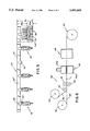
- FIG. 1 is a cross-sectional view of a prior art box contact mounted on a printed circuit board (PCB) and having its lower open end closed by a plug during wave soldering;
- PCB printed circuit board
- FIG. 2 is a top plane view, in schematic, illustrating a design which substantially eliminates underdesired solder wicking with standard wave soldering machines;
- FIG. 3 is side elevational view of a box contact in accordance with the present invention, in cross-section to illustrate the solder-resistant tape adhesively attached to a surface of the contact exposed to solder during wave soldering;
- FIG. 4 is a front elevational view of the contact shown in FIG. 3;
- FIG. 5 is a schematic representation of a plurality of box contacts in accordance with the present invention mounted on a continuous carrier, and showing, in broken outline, the continuous strip with tape attached thereto prior to die cutting and forming;
- FIG. 6 is a schematic representation of the method of producing box contact in accordance with the present invention.
- FIG. 3 a box contact in accordance with the present invention is generally designated by the reference numeral 18.
- the contact 18 has an upper contact portion 18a having a general uniform rectangular, typically square cross-section forming an interior space 18' which is open at the upper and lower ends of the contact portion 18a, as viewed in FIG. 3.
- the space 18' is dimensioned to receive a male contact member (not shown) through the upper open end.
- resilient to spring fingers F are formed from the sidewalls of the contact which protrude inwardly, best shown in FIG. 4.
- Mounting legs 18c are provided at the lower open end of the contact portion 18a, two mounting legs being shown which are spaced from each other and in opposing relationship. The mounting legs are spaced and dimensioned so as to be receivable through an opening in a printed circuit board in a conventional manner.
- a solder-resistant tape 20 is adhesively attached to a surface of the contact portion 18a within the interior space 18' at least in the region of lower open end. Tape 20 is resistant to molten solder during soldering to thereby mask the interior surface and prevent solder from wicking into adhering to the interior surface of the contact to thereby block the lower open end of the contact portion.
- the mounting legs 18c are not fully coated with the tape 20, a lower most portion 18d of the mounting legs being left uncovered.
- the tape includes an upper tape portion 20a that covers the lower surface of the contact portion 18a and 20b that covers the upper portion of the mounting leg 18c.
- the specific tape 20 that is used for the purpose of practicing the invention is not critical and almost any adhesive tape will provide the desired function.
- Numerous known tapes can be used for this purpose, including plastic tapes and paper tapes.
- inexpensive paper masking tapes have been found to have utility for this purpose.
- better quality tapes are available and should be used.
- Such tapes include polyimide and polyester films or tapes.
- Many such tapes are provided with adhesive systems which include silicone and are designed to resist solder at high temperatures.
- One such tape is marketed under the mark "CAPTON” is distributed by Specialty Tapes of Racine, Wis. and designated as tape No. CW-2210.
- the method of manufacturing box contacts in accordance with the present invention comprises the steps of providing a reel 32 from which there is advanced a continuous strip of metallic material 34 along a predetermined path as shown.
- the strip of metallic material has a predetermined width 35 (FIG. 5) and provided with a solderable surface and defines first and second longitudinal edges 35' and 35" as shown.
- a second reel 36 is provided with a continuous strip of solder-resistant tape 38 which is advanced along the same predetermined path, being guided by roller 40 into proximity with the metallic strip 34, both the strips being superimposed or juxtaposed with each other.
- the solder-resistant tape 40 is provided with an adhesive on a side facing the strip of metallic material and the two strips are pressed against each other by means of pressure rollers 42, 44 to form a single laminated strip.
- the strip of tape 38 has a width 35a smaller than the width 35 of the metallic strip.
- the strip of tape 38 covers a first continuous longitudinal surface portion of the metallic strip proximate to the first longitudinal edge 35', the lower edge as viewed in FIG. 5, to thereby leave exposed a second continuous longitudinal surface portion having a width 35b proximate to the second longitudinal edge 35", the upper edge as viewed in FIG. 5.
- the laminated tape L is directed through a die cutting machine 46 which may have a fixed body 46a and an upper punch or die cutting tool 46b that is periodically urged downwardly to die cut the laminated strip to provide the desired blanks or outlines of the box contacts.
- a reciprocating movable punch 46b any die cutting equipment can be used, including a circular die cutting tool or other like die cutting tools well known to those skilled in the art.
- the die cutting of the laminated strips forms the continuous strip 22 that includes the upper portions of the box contacts detachably connected to the continuous carrier 24 at the untaped second longitudinal surface portion and the taped lower portions of the box contacts and mounting legs.
- the lower portions of the box contacts and the mounting legs are at least partially covered with the solder-resistant tape to prevent wicking into and blocking of the lower open ends of the box contacts.
- the unit 48 shown in FIG. 6 is the forming device for converting the two-dimensional blanks shown on the right of FIG. 5 into the three-dimensional box contacts shown on the left of FIG. 5.
- the box contacts are attached to the carrier 24 and advantageously accumulated on a takeup reel 50.
- FIG. 5 a plurality of box contacts of the type shown in FIGS. 3 and 4 are shown integrally attached to a carrier strip 24 provided with sprocket holes 26 for use in connection with automated insertion equipment.
- Each of the contacts is connected to the carrier strip 24 by means of a frangible carrier tab 28 which is severed downstream by the insertion machine, as suggested at 28'.
- solder-resistant tape at the lower ends of the box contacts and the upper ends of the mounting legs, to provide solder-resistant surfaces proximate to the lower open ends of the box contacts, an inexpensive method can now be employed to produce contacts that can be used with new turbulent wave soldering machines while maintaining the low cost of production of such contacts.
Landscapes
- Engineering & Computer Science (AREA)
- Manufacturing & Machinery (AREA)
- Coupling Device And Connection With Printed Circuit (AREA)
Abstract
A box contact is disclosed which is coated on the interior surface thereof proximate to the lower open end as well as on the upper ends of the mounting legs with a solder-resistant tape to prevent solder from wicking into and blocking the lower open end of the contact portion. The method of producing such anti-wicking box contacts is also described.
Description
Divisional application of Ser. No. 08/124,977 filed on Sep. 21, 1993.
This invention generally relates to electrical connectors, and more specifically to a box contact for mounting on a printed circuit board which eliminates wicking during wave soldering, and method of manufacturing the electrical contact.
Box contacts that have substantially box shaped upper contact portions and downwardly extending mounting legs intended to pass through openings or holes in printed circuit boards are well-known and extensively used and have for many applications. Such box contacts generally have relatively large interior spaces into which there typically project a plurality of spring contacts intended to resiliently engage a male contact member inserted into the box contact. However, prior art designs require manual masking in order to prevent the entry of solder into the lower openings of the box contacts during wave soldering. The entry of the solder through the bottom opening of the box contact and subsequent hardening of the solder have presented problems since the solder interferes with the full insertion of the male contact and, additionally, may interfere with and in some cases substantially eliminate the resilient properties of the spring fingers or contacts.
Referring to FIG. 1, a conventional box contact of the type under discussion is generally designated by the reference numeral 10. The contact has an upper portion 10a which generally has a rectangular substantially uniform cross-section defining an interior space 11 as shown. Spring contacts or fingers 10b extend into the interior space of the box contact 10. Mounting legs 10c depend from the upper box portion 10a, with a small portion 10d of the mounting legs protruding beyond the printed circuit board 12. The protruding portions 10d are the portions of the mounting legs generally soldered to the lands or soldering pads (not shown) on the lower surface of the printed circuit board. Shown in dashed outline and designated by the letter S is a peak of molten solder which propagates through a wave-soldering machine in waves, as is well-known to those skilled in the art. In order to prevent the solder from entering through the lower open end of the box connector, a plug P or other masking scheme is commonly used. After wave-soldering, the solder mask or the plugs have to be removed.
Referring to FIG. 2, Zierick Manufacturing Corporation, the assignee of the present application, developed a box contact to eliminate masking and plugging of the holes useful for some wave-soldering applications. By selecting relative dimensions shown in FIG. 2, wherein the box B above the printed circuit board has dimensions greater than the dimensions of the aperture or hole 14 in the printed circuit board. Only relatively small mounting legs 10c extend through the hole so as to provide minimal metal within the area of the printed circuit board hole. Tests show and production runs confirm that this design prevents solder wicking if a standard wave soldering machine is used. However, with the introduction of surface mount technology, there are new turbulent wave-soldering machines for which the design suggested in FIG. 2 is not adequate.
Circuit board sockets have been disclosed for addressing this problem. For example, in U.S. Pat. No. 3,864,004, a socket is disclosed which has an inner surface of the body solder-resistant to prevent solder from flooding into the socket. However, in order to prevent solder from flooding and remaining in the socket, a solder-resist is used, such as a resistant aluminum oxide coating. The patent also suggests other alternative solder resists, such as chrome plate and a number of other commercially available resists. However, the use of solder resists that must be plated or deposited on a selected surface entails additional steps in the manufacturing process and this complicates the manufacturing process and makes the terminals more costly to manufacture. A pin and socket connector assembly utilizing a similar solder resist approach is disclosed in U.S. Pat. No. 3,222,632, and a circular board eyelet also utilizing a solder resist layer is disclosed in U.S. Pat. No. 4,070,077.
Accordingly, it is an object of the present invention to provide a box contact that eliminates solder wicking and which does not have the disadvantages inherent in comparable prior art contacts.
It is another object of the present invention to provide an anti-wicking box contact which is simple in construction and economical to manufacture.
It is another object of the present invention to provide a box contact of the type aforementioned which can be formed as a plurality of like box contacts detachably mounted on an elongate carrier.
It is yet another object of the present invention to provide a box contact as suggested in the previous objects which substantially simplifies the manufacture of an anti-wicking box contact and which optimizes the production thereof.
It is a further object of the present invention to provide a method of manufacturing box contacts of the type outlined in the previous objects.
In order to achieve the above objects, as well as others which will become apparent hereafter, a box contact for mounting on a printed circuit board having an opening comprises a contact portion having a general uniform rectangular cross-section forming an interior space open at upper and lower ends of said contact portion for receiving a male contact member through the upper end and mounting legs, at said lower open end, spaced to be receivable through the opening in the printed circuit board. A solder-resistant tape is adhesively attached to a surface of said contact portion within said interior space at least in the region of said lower open end. Said tape is resistive to molten solder to thereby mask said surface and prevent solder from wicking into and blocking said lower open end of said contact portion.
In accordance with the method of the present invention, a continuous strip of metallic material is advanced along a predetermined path. Said strip of metallic material has a predetermined width and is provided with a solderable surface and defines first and second longitudinal edges. A continuous strip of solder-resistant tape is advanced along said predetermined path and juxtaposed with said strip of metallic material. Said strip of tape has a width smaller than said predetermined width and is provided with adhesive on a side facing said strip of metallic material. Said strip of tape is attached to said metallic strip to cover a first continuous longitudinal surface portion of said metallic strip proximate to said first longitudinal edge to thereby leave exposed a second continuous longitudinal surface portion of said metallic strip proximate to said second longitudinal edge. Said attached strips are die cut and formed to form the upper portions of the box contacts detachably connected to a continuous carrier strip formed from said second longitudinal surface portion and lower portions of box contacts and mounting legs for each box contact from said second continuous longitudinal surface portion. In this manner, said lower portions of the box contacts and legs are at least partially covered with said solder-resistant tape to prevent wicking into and blocking a lower open end of the box contact.
Other objects and features of the invention will become apparent from the description that follows, taken in conjunction with the accompanying drawings illustrating the invention, in which:
FIG. 1 is a cross-sectional view of a prior art box contact mounted on a printed circuit board (PCB) and having its lower open end closed by a plug during wave soldering;
FIG. 2 is a top plane view, in schematic, illustrating a design which substantially eliminates underdesired solder wicking with standard wave soldering machines;
FIG. 3 is side elevational view of a box contact in accordance with the present invention, in cross-section to illustrate the solder-resistant tape adhesively attached to a surface of the contact exposed to solder during wave soldering;
FIG. 4 is a front elevational view of the contact shown in FIG. 3;
FIG. 5 is a schematic representation of a plurality of box contacts in accordance with the present invention mounted on a continuous carrier, and showing, in broken outline, the continuous strip with tape attached thereto prior to die cutting and forming; and
FIG. 6 is a schematic representation of the method of producing box contact in accordance with the present invention.
Referring now specifically to the drawings, in which identical or similar reference parts are designated by the same reference numerals throughout, and first referring to FIG. 3, a box contact in accordance with the present invention is generally designated by the reference numeral 18.
The contact 18 has an upper contact portion 18a having a general uniform rectangular, typically square cross-section forming an interior space 18' which is open at the upper and lower ends of the contact portion 18a, as viewed in FIG. 3. The space 18' is dimensioned to receive a male contact member (not shown) through the upper open end. As is common with such box contacts, resilient to spring fingers F are formed from the sidewalls of the contact which protrude inwardly, best shown in FIG. 4. Mounting legs 18c are provided at the lower open end of the contact portion 18a, two mounting legs being shown which are spaced from each other and in opposing relationship. The mounting legs are spaced and dimensioned so as to be receivable through an opening in a printed circuit board in a conventional manner.
A solder-resistant tape 20 is adhesively attached to a surface of the contact portion 18a within the interior space 18' at least in the region of lower open end. Tape 20 is resistant to molten solder during soldering to thereby mask the interior surface and prevent solder from wicking into adhering to the interior surface of the contact to thereby block the lower open end of the contact portion. In the embodiment shown, the mounting legs 18c are not fully coated with the tape 20, a lower most portion 18d of the mounting legs being left uncovered. However, the tape includes an upper tape portion 20a that covers the lower surface of the contact portion 18a and 20b that covers the upper portion of the mounting leg 18c. It is important, in the use of the invention, to coat the inwardly facing surfaces of the box contact in the region of the lower open end thereof where the molten solder has a tendency to enter and solidify. The application of solder to the lower most tip 18d of the mounting leg does not present a serious problem and, in that instant, results in a saving of tape. It is, of course, possible to coat the entire mounting leg with tape and this would, in most instances, be the preferable approach.
The specific tape 20 that is used for the purpose of practicing the invention is not critical and almost any adhesive tape will provide the desired function. Numerous known tapes can be used for this purpose, including plastic tapes and paper tapes. In fact, inexpensive paper masking tapes have been found to have utility for this purpose. However, in most instances, better quality tapes are available and should be used. Such tapes include polyimide and polyester films or tapes. Many such tapes are provided with adhesive systems which include silicone and are designed to resist solder at high temperatures. One such tape is marketed under the mark "CAPTON" is distributed by Specialty Tapes of Racine, Wis. and designated as tape No. CW-2210. Another tape marketed as style No. C690 under the mark "Temp-R-Tape" is distributed by the CHR Division of Furon of New Haven, Conn. Numerous film and paper tapes are marketed by TTI Industrial Division of Tesa Tuck, Inc. of Sparta, Mich. suitable film tapes being distributed under Model No. 428 and 4429, both of which are polyimide tapes. Tesa Tuck, Inc. also distributes a film under the designation "Tesafilm 4164 (R)" which is designed for conventional masking during wave soldering. Numerous tapes suitable for the purpose are also marketed by Ideal Tape Company of Lowell, Mass. many of which are polyester, polyimide and even paper/polyester laminates that are suitable for the intended purpose and are coated with various adhesives, including silicone and rubber.
The method of manufacturing box contacts in accordance with the present invention, referring to FIGS. 5 and 6, comprises the steps of providing a reel 32 from which there is advanced a continuous strip of metallic material 34 along a predetermined path as shown. The strip of metallic material has a predetermined width 35 (FIG. 5) and provided with a solderable surface and defines first and second longitudinal edges 35' and 35" as shown. A second reel 36 is provided with a continuous strip of solder-resistant tape 38 which is advanced along the same predetermined path, being guided by roller 40 into proximity with the metallic strip 34, both the strips being superimposed or juxtaposed with each other. The solder-resistant tape 40 is provided with an adhesive on a side facing the strip of metallic material and the two strips are pressed against each other by means of pressure rollers 42, 44 to form a single laminated strip. The strip of tape 38 has a width 35a smaller than the width 35 of the metallic strip. The strip of tape 38 covers a first continuous longitudinal surface portion of the metallic strip proximate to the first longitudinal edge 35', the lower edge as viewed in FIG. 5, to thereby leave exposed a second continuous longitudinal surface portion having a width 35b proximate to the second longitudinal edge 35", the upper edge as viewed in FIG. 5. The left side of FIG. 5 shows, in fragmented view, a portion of the strip prior to die cutting and forming, with the outline of the contact showing the lines where the contact is die cut from the continuous laminated strip. As illustrated in FIG. 6, the laminated tape L is directed through a die cutting machine 46 which may have a fixed body 46a and an upper punch or die cutting tool 46b that is periodically urged downwardly to die cut the laminated strip to provide the desired blanks or outlines of the box contacts. However, instead of a reciprocating movable punch 46b, any die cutting equipment can be used, including a circular die cutting tool or other like die cutting tools well known to those skilled in the art. The die cutting of the laminated strips forms the continuous strip 22 that includes the upper portions of the box contacts detachably connected to the continuous carrier 24 at the untaped second longitudinal surface portion and the taped lower portions of the box contacts and mounting legs. In this way, the lower portions of the box contacts and the mounting legs are at least partially covered with the solder-resistant tape to prevent wicking into and blocking of the lower open ends of the box contacts. The unit 48 shown in FIG. 6 is the forming device for converting the two-dimensional blanks shown on the right of FIG. 5 into the three-dimensional box contacts shown on the left of FIG. 5. The box contacts are attached to the carrier 24 and advantageously accumulated on a takeup reel 50.
In FIG. 5, a plurality of box contacts of the type shown in FIGS. 3 and 4 are shown integrally attached to a carrier strip 24 provided with sprocket holes 26 for use in connection with automated insertion equipment. Each of the contacts is connected to the carrier strip 24 by means of a frangible carrier tab 28 which is severed downstream by the insertion machine, as suggested at 28'.
With the introduction of solder-resistant tape at the lower ends of the box contacts and the upper ends of the mounting legs, to provide solder-resistant surfaces proximate to the lower open ends of the box contacts, an inexpensive method can now be employed to produce contacts that can be used with new turbulent wave soldering machines while maintaining the low cost of production of such contacts.
While there has been illustrated and described a preferred embodiment of the invention, it is understood that the invention is capable of modification and, therefore, the invention is not to be limited to the precise details set forth but the invention is intended only to be limited to the scope of the claims that follow.
Claims (2)
1. A method of manufacturing box contacts comprising the steps of advancing a continuous strip of metallic material along a predetermined path, said strip of metallic material having a predetermined width and provided with a solderable surface and defining first and second longitudinal edges; advancing a continuous strip of solder resistant tape along said predetermined path and juxtaposed with said strip of metallic material, said strip of tape having a width smaller than said predetermined width and provided with adhesive on a side facing said strip of metallic material; attaching said strip of tape to said metallic strip to cover a first continuous longitudinal surface portion of said metallic strip proximate to said first longitudinal edge to thereby leave exposed a second continuous longitudinal surface portion of said metallic strip proximate to said second longitudinal edge; die cutting and forming said attached strips to form upper portions of box contacts detachably connected to a continuous carrier strip formed from said second longitudinal surface portion and lower portions of box contacts and mounting legs for each box contact formed from said second continuous longitudinal surface portion, whereby said lower portions of the box contacts and mounting legs are at least partially covered with said solder resistant tape to prevent wicking into and blocking a lower open end of the box contact.
2. A method as defined in claim 1, wherein said step of adhesively attaching said strip includes the step of pressing said strips together.
Priority Applications (1)
| Application Number | Priority Date | Filing Date | Title |
|---|---|---|---|
| US08/349,975 US5495669A (en) | 1993-09-21 | 1994-12-06 | Method of making box contacts |
Applications Claiming Priority (2)
| Application Number | Priority Date | Filing Date | Title |
|---|---|---|---|
| US12497793A | 1993-09-21 | 1993-09-21 | |
| US08/349,975 US5495669A (en) | 1993-09-21 | 1994-12-06 | Method of making box contacts |
Related Parent Applications (1)
| Application Number | Title | Priority Date | Filing Date |
|---|---|---|---|
| US12497793A Division | 1993-09-21 | 1993-09-21 |
Publications (1)
| Publication Number | Publication Date |
|---|---|
| US5495669A true US5495669A (en) | 1996-03-05 |
Family
ID=22417681
Family Applications (1)
| Application Number | Title | Priority Date | Filing Date |
|---|---|---|---|
| US08/349,975 Expired - Lifetime US5495669A (en) | 1993-09-21 | 1994-12-06 | Method of making box contacts |
Country Status (1)
| Country | Link |
|---|---|
| US (1) | US5495669A (en) |
Cited By (10)
| Publication number | Priority date | Publication date | Assignee | Title |
|---|---|---|---|---|
| US5669126A (en) * | 1993-08-20 | 1997-09-23 | Murata Manufacturing Co., Ltd. | Process for manufacturing a terminal for a piezoelectric device |
| US5844308A (en) * | 1997-08-20 | 1998-12-01 | Cts Corporation | Integrated circuit anti-bridging leads design |
| US6707152B1 (en) * | 1999-04-16 | 2004-03-16 | Micron Technology, Inc. | Semiconductor device, electrical conductor system, and method of making |
| US20040224576A1 (en) * | 2001-02-13 | 2004-11-11 | Yazaki Corporation | Male terminal fitting and method of manufacturing the same |
| US20040229507A1 (en) * | 2002-10-25 | 2004-11-18 | Robert Stanford | Miniature contact block packaging for printed circuit |
| CN102185188A (en) * | 2009-12-21 | 2011-09-14 | 日立汽车系统株式会社 | Connector and method for producing the connector |
| US20110287666A1 (en) * | 2007-12-20 | 2011-11-24 | Molex Incorporated | Anti-wicking terminal and connector |
| US20150236465A1 (en) * | 2011-09-16 | 2015-08-20 | Wayne Cowan | Automated assembly of electrical connector |
| US10114039B1 (en) * | 2015-04-24 | 2018-10-30 | Johnstech International Corporation | Selectively geometric shaped contact pin for electronic component testing and method of fabrication |
| US20220209430A1 (en) * | 2020-12-29 | 2022-06-30 | Turck Inc. | Electrical contact, system and method for manufacturing an electrical contact |
Citations (6)
| Publication number | Priority date | Publication date | Assignee | Title |
|---|---|---|---|---|
| US3650706A (en) * | 1970-03-23 | 1972-03-21 | Amp Inc | Terminal tape and method for making the same |
| US4149768A (en) * | 1977-06-15 | 1979-04-17 | Amp Incorporated | Composite strip of thermoplastic articles and method of manufacturing same |
| US4241976A (en) * | 1979-07-20 | 1980-12-30 | International Telephone And Telegraph Corporation | Contact retention clip and method of inserting same in an insulator |
| US5073132A (en) * | 1989-02-28 | 1991-12-17 | Trw Daut & Rietz Gmbh & Co. Kg | Flat contact spring for plugs of electrical plug and socket connections |
| US5175928A (en) * | 1990-06-11 | 1993-01-05 | Amp Incorporated | Method of manufacturing an electrical connection assembly |
| US5274911A (en) * | 1991-10-21 | 1994-01-04 | American Shizuki Corporation | Electronic components with leads partly solder coated |
-
1994
- 1994-12-06 US US08/349,975 patent/US5495669A/en not_active Expired - Lifetime
Patent Citations (6)
| Publication number | Priority date | Publication date | Assignee | Title |
|---|---|---|---|---|
| US3650706A (en) * | 1970-03-23 | 1972-03-21 | Amp Inc | Terminal tape and method for making the same |
| US4149768A (en) * | 1977-06-15 | 1979-04-17 | Amp Incorporated | Composite strip of thermoplastic articles and method of manufacturing same |
| US4241976A (en) * | 1979-07-20 | 1980-12-30 | International Telephone And Telegraph Corporation | Contact retention clip and method of inserting same in an insulator |
| US5073132A (en) * | 1989-02-28 | 1991-12-17 | Trw Daut & Rietz Gmbh & Co. Kg | Flat contact spring for plugs of electrical plug and socket connections |
| US5175928A (en) * | 1990-06-11 | 1993-01-05 | Amp Incorporated | Method of manufacturing an electrical connection assembly |
| US5274911A (en) * | 1991-10-21 | 1994-01-04 | American Shizuki Corporation | Electronic components with leads partly solder coated |
Cited By (17)
| Publication number | Priority date | Publication date | Assignee | Title |
|---|---|---|---|---|
| US5669126A (en) * | 1993-08-20 | 1997-09-23 | Murata Manufacturing Co., Ltd. | Process for manufacturing a terminal for a piezoelectric device |
| US5844308A (en) * | 1997-08-20 | 1998-12-01 | Cts Corporation | Integrated circuit anti-bridging leads design |
| US6707152B1 (en) * | 1999-04-16 | 2004-03-16 | Micron Technology, Inc. | Semiconductor device, electrical conductor system, and method of making |
| US20040224576A1 (en) * | 2001-02-13 | 2004-11-11 | Yazaki Corporation | Male terminal fitting and method of manufacturing the same |
| US7114253B2 (en) * | 2001-02-13 | 2006-10-03 | Yazaki Corporation | Male terminal fitting and method of manufacturing the same |
| US20040229507A1 (en) * | 2002-10-25 | 2004-11-18 | Robert Stanford | Miniature contact block packaging for printed circuit |
| US7131192B2 (en) * | 2002-10-25 | 2006-11-07 | Motorola, Inc. | Method of manufacturing printed circuit boards using miniature contact block packagings |
| US20110287666A1 (en) * | 2007-12-20 | 2011-11-24 | Molex Incorporated | Anti-wicking terminal and connector |
| US8454397B2 (en) * | 2007-12-20 | 2013-06-04 | Molex Incorporated | Anti-wicking terminal and connector |
| CN102185188A (en) * | 2009-12-21 | 2011-09-14 | 日立汽车系统株式会社 | Connector and method for producing the connector |
| CN102185188B (en) * | 2009-12-21 | 2015-03-11 | 日立汽车系统株式会社 | Method for producing connector |
| US20150236465A1 (en) * | 2011-09-16 | 2015-08-20 | Wayne Cowan | Automated assembly of electrical connector |
| US9577397B2 (en) * | 2011-09-16 | 2017-02-21 | Apple Inc. | Method of manufacturing a shell assembly for an electrical connector |
| US10114039B1 (en) * | 2015-04-24 | 2018-10-30 | Johnstech International Corporation | Selectively geometric shaped contact pin for electronic component testing and method of fabrication |
| US11029335B1 (en) * | 2015-04-24 | 2021-06-08 | Johnstech International Corporation | Selectively geometric shaped contact pin for electronic component testing and method of fabrication |
| US20220209430A1 (en) * | 2020-12-29 | 2022-06-30 | Turck Inc. | Electrical contact, system and method for manufacturing an electrical contact |
| US11450974B2 (en) * | 2020-12-29 | 2022-09-20 | Turck Inc. | Electrical contact, system and method for manufacturing an electrical contact |
Similar Documents
| Publication | Publication Date | Title |
|---|---|---|
| US6379161B1 (en) | Method of making an electrical connector | |
| US5495669A (en) | Method of making box contacts | |
| US5184767A (en) | Non-wicking solder preform | |
| KR100550407B1 (en) | One Touch Connectors and One Touch Connector Assemblies | |
| GB1343852A (en) | Connector for printed circuit board | |
| US3754324A (en) | Solder resist | |
| US5357060A (en) | Pattern structure of a printed circuit board | |
| US4343083A (en) | Method of manufacturing flexible printed circuit sheets | |
| US5291179A (en) | Printed circuit board | |
| GB2304470A (en) | Device for mounting a component | |
| US5823801A (en) | Electrical connector having thin contacts with surface mount edges | |
| CA1235199A (en) | Lead member and method for fixing thereof | |
| US4185378A (en) | Method for attaching component leads to printed circuit base boards and printed circuit base board advantageously used for working said method | |
| US5376026A (en) | Method of mounting a tab type male terminal and an assembly of tab type male terminals | |
| GB2248345A (en) | Edge soldering of electronic components | |
| US4977668A (en) | Method of making socket connector | |
| US5443391A (en) | Electric wire-connecting terminal | |
| US20030216087A1 (en) | Board-to-board electrical connector and method for manufacturing same | |
| JPH07254775A (en) | Circuit board | |
| JPH02285602A (en) | Electronic part | |
| GB983846A (en) | Improvements in printed circuit and method of making the same | |
| GB1474504A (en) | Process for producing pre-oriented continuous yarns | |
| US4770296A (en) | Seal construction for electrical parts | |
| JP3648818B2 (en) | Electronic parts storage case for mounting | |
| JPH03106096A (en) | Manufacture of printed wiring board |
Legal Events
| Date | Code | Title | Description |
|---|---|---|---|
| AS | Assignment |
Owner name: ZIERICK MANUFACTURING CORPORATION Free format text: ASSIGNMENT OF ASSIGNORS INTEREST;ASSIGNORS:LEGRADY, JANOS;SEARLES, WILLIAM S.;REEL/FRAME:007261/0224 Effective date: 19941111 |
|
| STCF | Information on status: patent grant |
Free format text: PATENTED CASE |
|
| FEPP | Fee payment procedure |
Free format text: PAYOR NUMBER ASSIGNED (ORIGINAL EVENT CODE: ASPN); ENTITY STATUS OF PATENT OWNER: SMALL ENTITY |
|
| FPAY | Fee payment |
Year of fee payment: 4 |
|
| FPAY | Fee payment |
Year of fee payment: 8 |
|
| FPAY | Fee payment |
Year of fee payment: 12 |