US5448088A - Semiconductor integrated circuit having lengthened connection pins for connection to external wirings - Google Patents
Semiconductor integrated circuit having lengthened connection pins for connection to external wirings Download PDFInfo
- Publication number
- US5448088A US5448088A US08/258,230 US25823094A US5448088A US 5448088 A US5448088 A US 5448088A US 25823094 A US25823094 A US 25823094A US 5448088 A US5448088 A US 5448088A
- Authority
- US
- United States
- Prior art keywords
- wiring
- cell
- basic cells
- integrated circuit
- semiconductor integrated
- Prior art date
- Legal status (The legal status is an assumption and is not a legal conclusion. Google has not performed a legal analysis and makes no representation as to the accuracy of the status listed.)
- Expired - Lifetime
Links
- 239000004065 semiconductor Substances 0.000 title claims abstract description 58
- 239000010410 layer Substances 0.000 description 22
- 230000000694 effects Effects 0.000 description 9
- 238000009792 diffusion process Methods 0.000 description 6
- 238000004519 manufacturing process Methods 0.000 description 5
- 229910052751 metal Inorganic materials 0.000 description 4
- 239000002184 metal Substances 0.000 description 4
- 229910052782 aluminium Inorganic materials 0.000 description 2
- XAGFODPZIPBFFR-UHFFFAOYSA-N aluminium Chemical compound [Al] XAGFODPZIPBFFR-UHFFFAOYSA-N 0.000 description 2
- 238000010586 diagram Methods 0.000 description 2
- 239000002355 dual-layer Substances 0.000 description 2
- PCHJSUWPFVWCPO-UHFFFAOYSA-N gold Chemical compound [Au] PCHJSUWPFVWCPO-UHFFFAOYSA-N 0.000 description 2
- 229910052737 gold Inorganic materials 0.000 description 2
- 239000010931 gold Substances 0.000 description 2
- 238000012986 modification Methods 0.000 description 2
- 230000004048 modification Effects 0.000 description 2
- 229910021420 polycrystalline silicon Inorganic materials 0.000 description 2
- 229920005591 polysilicon Polymers 0.000 description 2
- 239000000758 substrate Substances 0.000 description 2
- 239000000872 buffer Substances 0.000 description 1
- 230000015556 catabolic process Effects 0.000 description 1
- 238000006731 degradation reaction Methods 0.000 description 1
- 230000010354 integration Effects 0.000 description 1
Images


Classifications
-
- H—ELECTRICITY
- H01—ELECTRIC ELEMENTS
- H01L—SEMICONDUCTOR DEVICES NOT COVERED BY CLASS H10
- H01L27/00—Devices consisting of a plurality of semiconductor or other solid-state components formed in or on a common substrate
- H01L27/02—Devices consisting of a plurality of semiconductor or other solid-state components formed in or on a common substrate including semiconductor components specially adapted for rectifying, oscillating, amplifying or switching and having potential barriers; including integrated passive circuit elements having potential barriers
- H01L27/04—Devices consisting of a plurality of semiconductor or other solid-state components formed in or on a common substrate including semiconductor components specially adapted for rectifying, oscillating, amplifying or switching and having potential barriers; including integrated passive circuit elements having potential barriers the substrate being a semiconductor body
- H01L27/10—Devices consisting of a plurality of semiconductor or other solid-state components formed in or on a common substrate including semiconductor components specially adapted for rectifying, oscillating, amplifying or switching and having potential barriers; including integrated passive circuit elements having potential barriers the substrate being a semiconductor body including a plurality of individual components in a repetitive configuration
- H01L27/118—Masterslice integrated circuits
- H01L27/11803—Masterslice integrated circuits using field effect technology
- H01L27/11807—CMOS gate arrays
Definitions
- the present invention relates to a gate array type semiconductor integrated circuit.
- FIG. 17 is a plan view showing a basic cell structure of a prior art gate array type semiconductor integrated circuit. As shown in FIG. 17, each of basic cells 1 is comprised of a pair of transistors, a PMOS transistor TP and an NMOS transistor TN.
- the PMOS transistor TP is made by forming a PMOS transistor gate 12 on a P + diffusion layer 17 while the NMOS transistor TN is made by forming an NMOS transistor gate 13 on an N + diffusion layer 18.
- the PMOS transistor gate 12 and the NMOS transistor gate 13 are electrically connected to each other by a connection pin 15.
- Reference numerals 11, 14 and 16 designate a power source, a ground and an insulating oxide film, respectively.
- FIG. 18 is a sectional view taken along the line II--II of FIG. 17.
- the PMOS transistor gate 12 is selectively formed on a semiconductor substrate 51, and an insulating film 53 is formed on the PMOS transistor gate 12 except for part of it. Then, the connection pin 15 is formed covering part of the insulating film 53 and the PMOS transistor gate 12 on which no portion of the insulating film 53 lies.
- the basic cells 1 are arranged in cell alignments 3 on a chip 5 and the cell alignments 3 are arranged in array with wiring regions 31 defined between adjacent ones of the cell alignments 3 to constitute a gate array type semiconductor integrated circuit.
- Reference numeral 6 designates input/output buffers, and reference numeral 7 designates bonding pads.
- a dense array of the basic cells 1 on the chip 5 constitute a gate array type semiconductor integrated circuit. In such a case, part of the basic cells 1 are used as wiring regions.
- a combination of several of the basic cells 1 can constitute a macro cell having a predetermined logic function.
- an NAND gate 10 receiving signals on input terminals A, B and C as shown in FIG. 21 consists of three PMOS transistors T1 to T3 and three NMOS transistors T4 to T6, as shown in FIG. 22.
- via-holes (marked with "x" in FIG. 23) are provided in predetermined points, and wiring L1 is provided between the basic cells 1, so that the NAND gate 10 shown in FIG. 21 working as a macro cell 2 can be implemented.
- a length of exemplary one of the basic cells 1 shown in FIG. 17 is equal to one-wiring pitch W1 determined by a minimum wiring interval in the semiconductor manufacturing technology.
- the basic cells 1 are arranged in row to constitute the cell alignments 3.
- intervals between adjacent ones of connection pins 15 in any of the cell alignments 3 are also all equal to the single wiring pitch W1.
- Adjacent ones of the cell alignments 3 define the wiring regions 31, and external wirings are provided between the separate basic cells 1, especially between the basic cells 1 in the separate cell alignments 3 by providing wirings in the wiring regions 31.
- the external wirings provided in the wiring regions 31 are usually of dual-layer system where one layer is used for lateral wiring (wiring in the X-direction) while the other layer is used for longitudinal wiring (wiring in Y-direction perpendicular to the X-direction). Electrical connection of the lateral wiring with the longitudinal wiring is established by forming via-holes in positions where both the wirings overlap with each other.
- metal layers of aluminum, gold or the like are often used, and polysilicon layers may be used.
- the basic cells 1 are configured and arranged in the afore-mentioned manner, and the lateral wiring and longitudinal wiring are provided in the wiring regions 31 for connections between the basic cells 1 formed in the separate cell alignments 3.
- wiring restrictions there arises the problem that relative positions in wiring patterns of the lateral and longitudinal wirings are restricted (referred to as “wiring restrictions” hereinafter).
- first wiring electrically connecting a basic cell 1A in a cell alignment 3A and a basic cell 1C in a cell alignment 3B and second wiring electrically connecting a basic cell 1B in the cell alignment 3A and a basic cell 1D in the cell alignment 3B are to be formed in the wiring region 31 defined between the cell alignments
- longitudinal wiring 42A, lateral wiring 41A and longitudinal wiring 42C are used for the first wiring while a longitudinal wiring 42B, lateral wiring 41B and longitudinal wiring 42D are used for the second wiring.
- the lateral wiring of one of the first and second wirings be divided in connecting the associated cells, or that a bypass wiring be formed by using other wiring regions.
- a length along the first direction of each of connection pins for external connection in the basic cells is not less than one-wiring pitch which is determined by a minimum wiring interval with respect to external wirings between the basic cells, and a distance along the first direction between the connection pins of adjacent ones of the basic cells in each of the cell alignments is not less than one-wiring pitch.
- the semiconductor integrated circuit further comprises at least one wiring region, where the external wirings are to be formed, provided between two of the cell alignments adjacent to each other.
- the wiring region is formed between any adjacent ones of the cell alignments.
- the cell alignments are sequentially formed in the second direction without space.
- the length of each of the connection pins is the one-wiring pitch while the distance between the connection pins is the one-wiring pitch.
- each of the basic cells has a CMOS structure comprised of an NMOS transistor and a PMOS transistor, a gate of the NMOS transistor and a gate of the PMOS transistor being electrically connected by a specified internal wiring; and each of the connection pins is formed on at least one of the gates of the NMOS transistor and PMOS transistor.
- the one-wiring pitch is determined by a minimum wiring interval to which a thickness of each of the external wirings is added, the length along the second direction of each of the connection pins is determined as a half of the length of each of the external wirings.
- internal wirings are provided among the basic cells in the same cell alignment so as to constitute a macro cell having a predetermined logic function.
- each of the basic cells has a CMOS structure comprised of an NMOS transistor and a PMOS transistor, a gate of the NMOS transistor and a gate of the PMOS transistor being electrically connected by a specified internal wiring; and each of the connection pins is formed on the predetermined internal wiring.
- the length of each of the connection pins is twice as long as the one-wiring pitch, namely, two-wiring pitch, while the distance between the connection pins is the one-wiring pitch.
- the cell alignments include first, second and third cell alignments sequentially formed in the second direction without space.
- FIG. 1 is a plan view showing a configuration of a basic cell of a gate array type semiconductor integrated circuit in accordance with a first preferred embodiment of the present invention
- FIG. 2 is a plan view showing details of a connection pin related to FIG. 1;
- FIG. 3 is a sectional view taken along the line I--I of FIG. 1;
- FIG. 4 is a plan view showing a configuration of a macro cell of the semiconductor integrated circuit in the first preferred embodiment
- FIG. 5 is a plan view showing an arrangement of cell alignments in the first preferred embodiment
- FIG. 6 is a plan view illustrating effects of the first preferred embodiment
- FIG. 7 is a plan view illustrating effects of the first preferred embodiment
- FIG. 8 is a plan view illustrating effects of the first preferred embodiment
- FIG. 9 is a plan view illustrating effects of the first preferred embodiment
- FIG. 10 is a plan view illustrating effects of the first preferred embodiment
- FIG. 11 is a plan view illustrating effects of the first preferred embodiment
- FIG. 12 is a plan view illustrating effects of the first preferred embodiment
- FIG. 13 is a plan view showing a structure of basic cells of a gate array type semiconductor integrated circuit of a second preferred embodiment according to the present invention.
- FIG. 14 is a plan view illustrating effects of the second preferred embodiment
- FIG. 15 is a plan view illustrating effects of the second preferred embodiment
- FIG. 16 is a plan view showing a configuration of a basic cell of a gate array type semiconductor integrated circuit according to the third preferred embodiment of the present invention.
- FIG. 17 is a plan view showing a configuration of a basic cell of a prior art gate array type semiconductor integrated circuit
- FIG. 18 is a sectional view taken along the line II--II of FIG. 17;
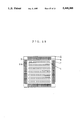
- FIG. 19 is a plan view showing the entire configuration of a gate array type semiconductor integrated circuit
- FIG. 20 is a plan view showing the entire configuration of a gate array type semiconductor integrated circuit
- FIG. 21 is a circuit diagram showing an NAND gate
- FIG. 22 is a circuit diagram showing an exemplary configuration of the NAND gate comprised of MOS transistors
- FIG. 23 is a plan view showing an exemplary configuration of the NAND gate in the gate array type semiconductor integrated circuit
- FIG. 24 is a plan view illustrating arrangements of cell alignments in a prior art gate array type semiconductor integrated circuit
- FIG. 25 is a plan view illustrating a disadvantage in the prior art.
- FIG. 26 is a plan view illustrating another disadvantage in the prior art.
- FIG. 1 is a plan view showing a structure of exemplary one of basic cells of a gate array type semiconductor integrated circuit in accordance with a first preferred embodiment of the present invention.
- each of basic cells 1 consists of a pair of transistors, a PMOS transistor TP and an NMOS transistor TN.
- the PMOS transistor TP is made by forming a PMOS transistor gate 12 on a P + diffusion layer 17 while the NMOS transistor TN is made by forming an NMOS transistor gate 13 on an N + diffusion layer 18.
- the PMOS transistor gate 12 and the NMOS transistor gate 13 are electrically connected by gate wiring 24, and connection pins 25 each having a lateral length (a length in X-direction of FIG. 1) of one-wiring pitch W1 are provided on top of the PMOS transistor gate 12 and that of the NMOS transistor gate 13.
- Reference numerals 11, 14 and 16 respectively designate a power source, a GND and an insulating oxide film.
- FIG. 2 is a plan view illustrating details of a plain configuration of an example of the connection pins 25 shown in FIG. 1.
- a longitudinal length (a length in Y-direction in FIG. 1) of each of the connection pins 25 equals a thickness "b" of metal wiring while its lateral length is precisely that which equals the one-wiring pitch W1 extended by b/2 from its opposite terminals to both the left and right.
- FIG. 3 is a sectional view taken along the line I--I of FIG. 1.
- the PMOS transistor gate 12 is selectively formed on a semiconductor substrate 51, and an insulating film 53 is formed over the entire surface except for part of the PMOS transistor gate 12.
- the connection pin 25 is formed, lying on the PMOS transistor gate 12 and onto the insulating film 53.
- the one-wiring pitch W1 shall be defined as a length determined by a minimum wiring interval in the semiconductor manufacturing technology allowing for a thickness of metal wiring.
- external wiring may be formed in one of the connection pins 25 formed on the PMOS transistor gate 12 and on the NMOS transistor gate 13, only one connection pin, namely the representative connection pin 25 alone, for any of the basic cells 1 will be shown in the drawings referred to hereinafter.
- basic cells 1 are arranged in row on a chip 5 to constitute cell alignments 3 as shown in FIG. 19, and the cell alignments are arranged with wiring regions 31 defined between adjacent ones of the cell alignments to constitute a gate array type semiconductor integrated circuit.
- the basic cells 1 are closely arranged in a dense array on the chip 5 as shown in FIG. 20 to constitute a gate array type semiconductor integrated circuit. In such a case, part of the basic cells 1 are used as wiring regions.
- FIG. 4 is a plan view showing a macro cell consisting of the basic cells 1 shown in FIG. 1. As shown in FIG. 4, the basic cells 1 are arranged in row to constitute a cell alignment, and via-holes (marked with blackened squares in FIG. 4) are provided in predetermined locations in the cell alignment and wiring L1 is provided among the basic cells to construct an NAND gate 10 of FIG. 21 in a macro cell 2.
- the basic cells 1 are arranged in row to constitute the cell alignments 3, and a distance in X-direction (a direction along each of the cell alignments 3) between the connection pins 25 of adjacent ones of the basic cells 1 in each of the cell alignments 3 is determined as the one-wiring pitch W1.
- connection pins 25 in any of the cell alignments 3 and their respective counterparts in the adjacent cell alignment, opposed to each other, are positioned in the same X coordinates.
- Regions defined between the cell alignments 3 opposed to each other are the wiring regions 31, and wiring is provided in the wiring regions 31 to provide external wiring between the separate basic cells 1, especially between the basic cells 1 in the separate cell alignments 3.
- wiring provided in the wiring regions 31 usually dual layer wiring is employed where lateral wiring (wiring in the X-direction) is provided in one layer or a first layer while longitudinal wiring (wiring in Y-direction perpendicular to the X-direction) is provided in the other layer or a second layer.
- connection of the lateral wiring to the longitudinal wiring is established by forming via-holes in areas where both the wirings overlap with each other.
- Wring layers used to provide the wirings are often made of metal such as aluminum, gold and the like, and sometimes they are made of polysilicon.
- the connection pins 25 are formed in the first layer.
- the gate array type semiconductor integrated circuit is designed in such a way that the lateral length of the connection pin 25 of each of the basic cells 1 is determined as the one-wiring pitch W1 while the distance between the connection pins 25 of adjacent ones of the basic cells in any of the cell alignments 3 is determined as the one-wiring pitch W1.
- first wiring electrically connecting a basic cell 1A in a cell alignment 3A and a basic cell 1D in a cell alignment 3B and second wiring electrically connecting a basic cell 1B in the cell alignment 3A and a basic cell 1C in the cell alignment 3B, are to be provided.
- the external wirings are formed by providing a longitudinal wiring 42A extending from the left terminal of the connection pin 25 in the basic cell 1A, a longitudinal wiring 42B extending from the left terminal of the connection pin 25 in the basic cell 1B, a longitudinal wiring 42C extending from the right terminal of the connection pin 25 in the basic cell 1C, and a longitudinal wiring 42D extending from the right terminal of the connection pin 25 of the basic cell 1D, and further forming a lateral wiring 41A and a lateral wiring 41B of which Y coordinates are not coincident with each other to connect the longitudinal wiring 42A with the longitudinal wiring 42D, and the longitudinal wiring 42B with the longitudinal wiring 42C, respectively.
- the external wirings can be formed by providing the longitudinal wiring 42A extending from the left terminal of the connection pin 25 in the basic cell 1A to the left terminal of the connection pin 25 in the basic cell 1C and the longitudinal wiring 42B extending from the left terminal of the connection pin 25 in the basic cell 1B to the left terminal of the connection pin 25 in the basic cell 1D, as shown in FIG. 7.
- a longitudinal wiring 44 is formed in the second layer while the connection pins 25 are formed in the first layer, and therefore, as shown in FIG. 8, another longitudinal wiring 44 can traverse the right terminal of the connection pin 25 not used for connection.
- longitudinal wiring 43A extending from the connection pin 25 in the cell alignment 3A can be provided in a wiring region 31A, traversing the cell alignment 3B without overlapping with the longitudinal wiring 42B in the cell alignment 3B, and also a longitudinal wiring 43B extending from the connection pin 25 in the cell alignment 3A can be formed in a wiring region 31B, traversing the cell alignment 3C without overlapping with the longitudinal wiring 42C in the cell alignment 3C.
- the longitudinal wiring of the basic cell 1 in one of the cell alignments 3 and that of the basic cell 1 in the other of the cell alignments 3 in the wiring region 31 between the cell alignments 3 opposed to each other are provided with one-wiring pitch W1 shifted from each other to make it utterly impossible that there is electrical connection between those longitudinal wrings in both the cell alignments 3 even if Y coordinates of the longitudinal wirings overlap with each other.
- the wiring regions 31 may be formed in a longitudinal length across which XN lateral wirings can be formed. In this way, the desirable longitudinal length for each of the wiring regions 31 can be easily found by calculating the overlap frequency XN of the lateral wirings.
- connection pins 25 As a lateral length of each of the connection pins 25 is increased, there is extra extension of a distance between the basic cells 1 which is to work as a transistor area; and therefore, possibility of breaking the wirings because of wiring level difference is reduced, and the yield in manufacturing process is enhanced.
- FIG. 10 shows an arrangement where the distance between the adjacent basic cells 1 in one cell alignment equals two-wiring pitch W2.
- one longitudinal wiring 42 can be formed extending from each of the basic cells 1, and since overlap of Y coordinates of the longitudinal wirings 42 of the basic cells 1 of the same X coordinate necessarily leads to electrical connection between the longitudinal wirings, there is no relaxation of the wiring restrictions as have existed in the prior art.
- FIG. 11 depicts an arrangement where the distance between the adjacent basic cells 1 in one cell alignment equals two-wiring pitch W2 and the basic cells 1 in a cell alignment 3A and their respective counterparts in a cell alignment 3B which is opposed to the cell alignment 3A with the wiring region 31 interposed therebetween are located in skew positions from each other, one-wiring pitch W1 shifted from face-to-face positions in the X-direction.
- the wiring restrictions can be relaxed to some extent, wiring paths are bent in providing any external wiring between the basic cells 1 in the cell alignment 3A and their respective counterparts in the cell alignment 3B, and hence, it is necessary to provide a lateral wiring 41.
- wiring patterns consisting of the longitudinal and lateral wirings become more complicated than required and the number of via-holes electrically connecting the longitudinal wirings and the lateral wirings is increased, and therefore, this example is not practical because of the degraded yield in providing wirings.
- FIG. 12 illustrates an arrangement where intervals between the adjacent basic cells 1 are variable so as to make the wiring restrictions avoidable. Although the wiring restrictions can be relaxed to some extent with such an arrangement, this example is unfeasible because numerous kinds of macro cells are to be registered in the macro cell library.
- connection pins 25 are formed on the PMOS transistor gate 12 and the NMOS transistor gate 13 in the above-mentioned first preferred embodiment, the connection pins 25 may be formed only on one of the gates 12 and 13.
- FIG. 13 is a plan view showing a basic cell arrangement of a gate array type semiconductor integrated circuit of a second preferred embodiment according to the present invention. As shown in FIG. 13, a lateral length of a connection pin 26 in each of basic cells 1 is twice as long as one-wiring pitch W1, namely, two-wiring pitch W2.
- connection pins 26 in the adjacent basic cells 1 in each of cell alignments 3 equals the one-wiring pitch W1 as in the first preferred embodiment.
- Other parts are similar to corresponding ones described in conjunction with the first preferred embodiment, and therefore, description about them is omitted.
- the gate array type semiconductor integrated circuit is designed in the conditions that the lateral length of the connection pin 26 of each of the basic cells 1 is determined as two-wiring pitch W2 and that the distance between the connection pints 26 of the adjacent basic cells in any of the cell alignments 3 is determined as one-wiring pitch W1.
- the wiring restrictions can be greatly relaxed, a coefficient of utilization of the basic cells 1 can be enhanced, and the yield in the manufacturing process can be enhanced, as in the first preferred embodiment.
- the semiconductor integrated circuit of the second preferred embodiment is superior in relaxation of the wiring restrictions to that of the first preferred embodiment. As shown in FIG.
- the wiring restrictions can be more relaxed than the semiconductor integrated circuit of the first preferred embodiment.
- FIG. 16 is a plan view showing a basic cell arrangement of a gate array type semiconductor integrated circuit of a third preferred embodiment according to the present invention.
- each of basic cells 1 consists of a pair of transistors, a PMOS transistor TP and an NMOS transistor TN.
- the PMOS transistor TP is made by forming a PMOS transistor gate 12 on a P + diffusion layer 17 while the NMOS transistor TN is made by forming an NMOS transistor gate 13 on an N + diffusion layer 18.
- the PMOS transistor gate 12 and the NMOS transistor gate 13 are electrically connected to each other by a gate wiring 24 interposed therebetween, and a connection pin 27 having a lateral length (a length in X-direction in FIG. 16) of one-wiring pitch W1 is provided on the gate wiring 24, electrically connected to the gate wiring 24.
- a distance between the connection pins 27 in adjacent ones of the basic cells 1 in each of cell alignments 3 is determined as one-wiring pitch W1.
- Other parts of this arrangement are similar to those in the first preferred embodiment, and therefore, description about them is omitted.
- the gate array type semiconductor integrated circuits are designed in the conditions that the lateral length of the connection pin 25 (27) in each of the basic cells 1 is determined as the one-wiring pitch W1 and that the distance between the connection pins 25 (27) of any adjacent basic cells in one of the cell alignments 3 is determined as the one-wiring pitch W1
- the gate array type semiconductor integrated circuit is designed in the conditions that the lateral length of the connection pin 26 in each of the basic cells 1 is determined as the two-wiring pitch W2 and that the distance between the connection pins 26 in any adjacent basic cells in any of the cell alignments 3 is determined as the one-wiring pitch W1.
- the present invention is not restricted to the precise form in the previous statement and will be effective if satisfying requirements stated below.
- the lateral length of the connection pin in each of the basic cells 1 may be determined as one-wiring pitch or over while the distance between the connection pins in adjacent ones of the basic cells 1 in any of the cell alignments 3 may be determined as the one-wiring pitch or over. This is because two or more longitudinal wirings can be formed extending from any connection pin in the basic cells 1 as external wirings.
- connection pins are determined as the one-wiring pitch W1 to minimize the degradation of integration of the semiconductor integrated circuits, and additionally, the lateral length of any connection pin is desirably determined as at most the two-wiring pitch W2 or so.
- connection pins are formed in the first layer where the lateral wiring is provided, they may also be formed in any layer other than the first and second layers.
- a length along a first direction of a connection pin for external connection in each of basic cells is one-wiring pitch or over, which is determined by a minimum wiring interval of external wirings among the basic cells, and a distance along the first direction between the connection pins in adjacent ones of the basic cells in any of cell alignments is the one-wiring pitch or over.
- connection pin in each of the basic cells Since two or more longitudinal wirings can be formed extending from the connection pin in each of the basic cells in a second direction, wiring restrictions upon connection pins in the separate basic cells can be greatly relaxed, and wiring among the basic cells can be relatively easily implemented.
Landscapes
- Engineering & Computer Science (AREA)
- Power Engineering (AREA)
- Physics & Mathematics (AREA)
- Condensed Matter Physics & Semiconductors (AREA)
- General Physics & Mathematics (AREA)
- Computer Hardware Design (AREA)
- Microelectronics & Electronic Packaging (AREA)
- Design And Manufacture Of Integrated Circuits (AREA)
Abstract
Description
Claims (12)
Applications Claiming Priority (2)
| Application Number | Priority Date | Filing Date | Title |
|---|---|---|---|
| JP5-163525 | 1993-07-01 | ||
| JP16352593A JP3289999B2 (en) | 1993-07-01 | 1993-07-01 | Semiconductor integrated circuit |
Publications (1)
| Publication Number | Publication Date |
|---|---|
| US5448088A true US5448088A (en) | 1995-09-05 |
Family
ID=15775531
Family Applications (1)
| Application Number | Title | Priority Date | Filing Date |
|---|---|---|---|
| US08/258,230 Expired - Lifetime US5448088A (en) | 1993-07-01 | 1994-06-10 | Semiconductor integrated circuit having lengthened connection pins for connection to external wirings |
Country Status (2)
| Country | Link |
|---|---|
| US (1) | US5448088A (en) |
| JP (1) | JP3289999B2 (en) |
Cited By (6)
| Publication number | Priority date | Publication date | Assignee | Title |
|---|---|---|---|---|
| US5751015A (en) * | 1995-11-17 | 1998-05-12 | Micron Technology, Inc. | Semiconductor reliability test chip |
| US20060136848A1 (en) * | 2004-12-20 | 2006-06-22 | Matsushita Electric Industrial Co., Ltd. | Cell, standard cell, standard cell library, a placement method using standard cell, and a semiconductor integrated circuit |
| US20100127378A1 (en) * | 2008-11-21 | 2010-05-27 | Koji Higuchi | Semiconductor device and semiconductor package |
| US7802208B1 (en) * | 2004-06-07 | 2010-09-21 | Pulsic Limited | Design automation using spine routing |
| WO2015054536A1 (en) * | 2013-10-09 | 2015-04-16 | Synopsys Taiwan Co., LTD. | Spine routing with multiple main spines |
| TWI579988B (en) * | 2010-11-29 | 2017-04-21 | Synopsys Inc | Multiple level spine routing |
Citations (2)
| Publication number | Priority date | Publication date | Assignee | Title |
|---|---|---|---|---|
| JPH0442571A (en) * | 1990-06-08 | 1992-02-13 | Mitsubishi Electric Corp | Method for arranging integrated circuit element in semiconductor integrated circuit device |
| JPH04287369A (en) * | 1991-03-15 | 1992-10-12 | Sharp Corp | Manufacture of gate array and semiconductor integrated circuit device |
-
1993
- 1993-07-01 JP JP16352593A patent/JP3289999B2/en not_active Expired - Lifetime
-
1994
- 1994-06-10 US US08/258,230 patent/US5448088A/en not_active Expired - Lifetime
Patent Citations (2)
| Publication number | Priority date | Publication date | Assignee | Title |
|---|---|---|---|---|
| JPH0442571A (en) * | 1990-06-08 | 1992-02-13 | Mitsubishi Electric Corp | Method for arranging integrated circuit element in semiconductor integrated circuit device |
| JPH04287369A (en) * | 1991-03-15 | 1992-10-12 | Sharp Corp | Manufacture of gate array and semiconductor integrated circuit device |
Cited By (15)
| Publication number | Priority date | Publication date | Assignee | Title |
|---|---|---|---|---|
| US5936260A (en) * | 1995-11-17 | 1999-08-10 | Micron Technology, Inc. | Semiconductor reliability test chip |
| US6157046A (en) * | 1995-11-17 | 2000-12-05 | Micron Technology, Inc. | Semiconductor reliability test chip |
| US6320201B1 (en) | 1995-11-17 | 2001-11-20 | Micron Technology, Inc. | Semiconductor reliability test chip |
| US6538264B2 (en) | 1995-11-17 | 2003-03-25 | Micron Technology, Inc. | Semiconductor reliability test chip |
| US6770906B2 (en) | 1995-11-17 | 2004-08-03 | Micron Technology, Inc. | Semiconductor reliability test chip |
| US5751015A (en) * | 1995-11-17 | 1998-05-12 | Micron Technology, Inc. | Semiconductor reliability test chip |
| US7802208B1 (en) * | 2004-06-07 | 2010-09-21 | Pulsic Limited | Design automation using spine routing |
| US8479141B1 (en) | 2004-06-07 | 2013-07-02 | Pulsic Limited | Automation using spine routing |
| US20060136848A1 (en) * | 2004-12-20 | 2006-06-22 | Matsushita Electric Industrial Co., Ltd. | Cell, standard cell, standard cell library, a placement method using standard cell, and a semiconductor integrated circuit |
| US20090138840A1 (en) * | 2004-12-20 | 2009-05-28 | Panasonic Corporation | Cell, standard cell, standard cell library, a placement method using standard cell, and a semiconductor integrated circuit |
| US7503026B2 (en) | 2004-12-20 | 2009-03-10 | Panasonic Corporation | Cell, standard cell, standard cell library, a placement method using standard cell, and a semiconductor integrated circuit |
| US20100127378A1 (en) * | 2008-11-21 | 2010-05-27 | Koji Higuchi | Semiconductor device and semiconductor package |
| US8860204B2 (en) * | 2008-11-21 | 2014-10-14 | Oki Semiconductor Co., Ltd. | Semiconductor device and package with bit cells and power supply electrodes |
| TWI579988B (en) * | 2010-11-29 | 2017-04-21 | Synopsys Inc | Multiple level spine routing |
| WO2015054536A1 (en) * | 2013-10-09 | 2015-04-16 | Synopsys Taiwan Co., LTD. | Spine routing with multiple main spines |
Also Published As
| Publication number | Publication date |
|---|---|
| JPH0722598A (en) | 1995-01-24 |
| JP3289999B2 (en) | 2002-06-10 |
Similar Documents
| Publication | Publication Date | Title |
|---|---|---|
| US4811073A (en) | Gate array arrangement | |
| JP3154411B2 (en) | Two metal layer integrated circuit gate array laid out by CAD | |
| US9691678B2 (en) | Semiconductor device having electrode pads arranged between groups of external electrodes | |
| US5401989A (en) | Semiconductor device having a basic cell region and an I/O cell region defined on a surface thereof | |
| IE53844B1 (en) | Semiconductor integrated circuit comprising a semiconductor substrate and interconnecting layers | |
| KR20000070614A (en) | Power/ground metallization routing in a semiconductor device | |
| US5227649A (en) | Circuit layout and method for VLSI circuits having local interconnects | |
| JP3917683B2 (en) | Semiconductor integrated circuit device | |
| US5448088A (en) | Semiconductor integrated circuit having lengthened connection pins for connection to external wirings | |
| US20030034539A1 (en) | Semiconductor integrated circuit device | |
| US5434436A (en) | Master-slice type semiconductor integrated circuit device having multi-power supply voltage | |
| US6476425B1 (en) | Master-slice system semiconductor integrated circuit and design method thereof | |
| KR910007900B1 (en) | Semiconductor integrated circuit device | |
| US4853562A (en) | Programmable logic array using single transistor to generate true or complement signal | |
| USH512H (en) | Automated universal array | |
| KR100255060B1 (en) | Semiconductor device | |
| US5323033A (en) | Single chip IC device having gate array or memory with gate array and provided with redundancy capability | |
| US7245027B2 (en) | Apparatus and method for signal bus line layout in semiconductor device | |
| JP2001156178A (en) | Semiconductor device and automatic layout method for the same | |
| US10833011B2 (en) | Semiconductor device | |
| US6903620B2 (en) | Circuit configuration for setting the input resistance and the input capacitance of an integrated semiconductor circuit chip | |
| JPH0534832B2 (en) | ||
| KR100648752B1 (en) | Integrated semiconductor circuit with a pad | |
| JP2529342B2 (en) | Channel wiring method | |
| EP0425032A1 (en) | Integrated CMOS circuit |
Legal Events
| Date | Code | Title | Description |
|---|---|---|---|
| AS | Assignment |
Owner name: MITSUBISHI ELECTRIC ENGINEERING CO., LTD., JAPAN Free format text: ASSIGNMENT OF ASSIGNORS INTEREST;ASSIGNORS:NAGAI, TAKAO;KANEKO, KOICHI;SHINAGAWA, HIROAKI;AND OTHERS;REEL/FRAME:007329/0318 Effective date: 19940523 Owner name: MITSUBISHI DENKI KABUSHIKI KAISHA, JAPAN Free format text: ASSIGNMENT OF ASSIGNORS INTEREST;ASSIGNORS:NAGAI, TAKAO;KANEKO, KOICHI;SHINAGAWA, HIROAKI;AND OTHERS;REEL/FRAME:007329/0318 Effective date: 19940523 |
|
| STCF | Information on status: patent grant |
Free format text: PATENTED CASE |
|
| FEPP | Fee payment procedure |
Free format text: PAYOR NUMBER ASSIGNED (ORIGINAL EVENT CODE: ASPN); ENTITY STATUS OF PATENT OWNER: LARGE ENTITY |
|
| FPAY | Fee payment |
Year of fee payment: 4 |
|
| FPAY | Fee payment |
Year of fee payment: 8 |
|
| FPAY | Fee payment |
Year of fee payment: 12 |
|
| AS | Assignment |
Owner name: RENESAS ELECTRONICS CORPORATION, JAPAN Free format text: ASSIGNMENT OF ASSIGNORS INTEREST;ASSIGNOR:MITSUBISHI DENKI KABUSHIKI KAISHA;REEL/FRAME:025980/0219 Effective date: 20110307 |