US5442328A - Transmission line correction system - Google Patents
Transmission line correction system Download PDFInfo
- Publication number
- US5442328A US5442328A US07/999,374 US99937492A US5442328A US 5442328 A US5442328 A US 5442328A US 99937492 A US99937492 A US 99937492A US 5442328 A US5442328 A US 5442328A
- Authority
- US
- United States
- Prior art keywords
- signal
- frequency
- amplitude
- correction
- transmission lines
- Prior art date
- Legal status (The legal status is an assumption and is not a legal conclusion. Google has not performed a legal analysis and makes no representation as to the accuracy of the status listed.)
- Expired - Lifetime
Links
Images


Classifications
-
- H—ELECTRICITY
- H04—ELECTRIC COMMUNICATION TECHNIQUE
- H04B—TRANSMISSION
- H04B3/00—Line transmission systems
- H04B3/02—Details
- H04B3/04—Control of transmission; Equalising
- H04B3/14—Control of transmission; Equalising characterised by the equalising network used
- H04B3/143—Control of transmission; Equalising characterised by the equalising network used using amplitude-frequency equalisers
- H04B3/145—Control of transmission; Equalising characterised by the equalising network used using amplitude-frequency equalisers variable equalisers
-
- H—ELECTRICITY
- H04—ELECTRIC COMMUNICATION TECHNIQUE
- H04N—PICTORIAL COMMUNICATION, e.g. TELEVISION
- H04N7/00—Television systems
- H04N7/10—Adaptations for transmission by electrical cable
- H04N7/102—Circuits therefor, e.g. noise reducers, equalisers, amplifiers
Definitions
- the present invention relates to a transmission line correction device.
- Transmission lines are employed generally in the telecommunications field, their purpose being to transfer an electrical signal from one point to another point. This can for example involve transmitting a video signal from a camera head to a mobile outside broadcast vehicle, or, again, between two blocks of buildings.
- lines of the same type and length for example coaxial cable constituted by the same elements, there is nevertheless a variation in attenuation from one line to an other. This is due to the fact that the elements constituting such lines are not strictly identical and nor are they associated in a strictly identical manner.
- amplitude correction to denote amplitude correction applied to a DC signal or to the DC component of any signal whatsoever.
- correction for frequency we shall use the expression “correction for frequency” to denote the process of correcting the amplitude of a frequency signal for the components at different frequencies of any given signal.
- correction systems work on the basis of switching in so called correction cells. Such systems correct defects in amplitude and frequency brought about by propagation. These correction cells are built up from discrete components such as resistors, self-inductances or capacitors. Such correction systems must be located at precise points in the transmission line as they are designed to be able to correct defects in the line over a given length. The individual components constituting such cells are adjusted manually. This is disadvantageous as such adjustments are time consuming and difficult to get right. It is hence practically impossible to rapidly and cheaply adjust a system composed of several transmission lines in parallel.
- the present invention does not suffer from the above disadvantages.
- the present invention provides a correction system for transmission lines comprising means adapted to automatically correct the attenuation of the DC component of any signal traveling on said line and means adapted to correct the attenuation of the various frequency components of said signal, said means adapted to correct the attenuation of frequency components comprising automatic correction means.
- the present invention also provides system for correcting a plurality of transmission lines comprising means for correcting the spread in attenuation of the DC components and the frequency components of the various signals traveling on said plurality of lines wherein said attenuation spread correcting means comprise automatic DC component and frequency component correction means.
- One advantage of the invention is hence that of being able to provide automatic correction, both as regards amplitude and for frequency, of variations in attenuation that the signal is subject to in the lines.
- FIG. 1 shows attenuation curves A for three transmission lines of the same type and the same length as a function of the frequency f of the transmitted signal, in the absence of any correction.
- FIG. 2A is a block diagram of an automatic line correcting system in accordance with the prior art.
- FIG. 2B shows the attenuation curves A for three transmission lines of the same type and the same length as a function of the frequence f of the signal, in the case where the lines are corrected by means of a line correction system described in FIG. 2A.
- FIG. 3A is a block diagram of a line correction system according to the preferred embodiment of the invention.
- FIG. 3B shows the attenuation curves A for three transmission lines of the same type and the same length as a function of the frequence f of the signal, in the case where the lines are corrected by means of a line correction system described in FIG. 3A.
- FIG. 3C shows the attenuation curves A for three transmission lines of the same type and the same length as a function of the frequence f of the signal, in accordance with another embodiment of the invention.
- FIG. 4 shows one application of the correction system according to the invention.
- FIG. 1 shows attenuation curves A for three transmission lines of the same type and the same length as a function of the frequency f of the transmitted signal, in the absence of any correction.
- Curve C1 (L1) relates to a line L1
- curve C2 (L2) relates to a line L2 and curve C3 (L3) to a line L3.
- the attenuation A differs from one line to another.
- lines L1, L2 and L3 introduce attenuations of respectively A1, A2 and A3.
- attenuation evolves differently from one line to the other.
- One can thus for example find a differential attenuation ⁇ A of some 3 decibels between two transmission lines of the same type (L1 and L3), each having 100 meters long and carrying an identical signal of frequency f o 10 MHZ.
- FIG. 2A is a block diagram of an automatic line correction system in accordances with the prior art.
- the points E and F are the input of the system and the points U and V are the output.
- a fraction F1 of the signal S is taken off at the output from the correction system, signal F1 being for example extracted by a switch 21.
- switch 21 When switch 21 is closed, the detected voltage, for example across the terminals of capacitor C1, is a measure of the DC component of the signal.
- the detected voltage is then fed to a comparator 1 which compares it with a reference value R in order to generate a gain correction value v.
- the gain correction value v is used to control a multiplier 2 the multiplication factor K2 of which, applied to the signal Sa traveling along the line portion La, makes it possible to adjust the amplitude of output signal S to the correct value via the differential amplifier 3.
- the signal from multiplier 2 is fed to the positive terminal of the differential amplifier 3 having linear gain G2.
- a fractional part F2 of signal Sa is taken off from line portion La and this part of signal F2 is fed to a high-pass filter 5 which is set to provide correction for frequency of the line's attenuation curve, in accordance with the desired law.
- This law can be such, for example, that the slope of the attenuation curve for signal S as a function of frequency is zero.
- the gain correction value v is applied to a multiplier of multiplication factor K1.
- the signal from multiplier 4 is then fed to the negative terminal of differential amplifier 3, thus providing correct frequency response adjustment of the transmission line.
- the frequency correcting filters 5 consist of self-inductances and capacitors.
- the upper cutoff frequency of the transmission line can reach high values, for example 500 MHz.
- Those skilled in the art know that it is then necessary to employ a large number of self-inductances and capacitors in order to cover a frequency response extending over such a wide band.
- the self-inductances and capacitors require manual adjustment, correction for frequency of the line is, under such conditions, a time consuming operation which is difficult to perform correctly.
- FIG. 2B shows the attenuation curves A for three transmission lines of the same type and the same length as a function of the frequence f of the signal, in the case where the lines are corrected by means of a line correction system described in FIG. 2A.
- all the curves (C11 (L1), C21 (L2), C31 (L3)) pass through the same point P.
- Curve C21 (L2) represents the attenuation of a line L2.
- filter 5 allowing correction for frequency has been adjusted to provide zero slope of attenuation as a function of frequency. Adjustment is manual, and thus tricky to perform.
- FIG. 3A shows a block diagram of a line correcting system according to the preferred embodiment of the invention.
- the points E and F constitute the input to the system, and the points U and V the output.
- an amplitude correction loop is provided using, as reference value R1, a signal portion of a calibrated level. This portion can for example be the bottom of the video synchronizing signal making it possible to provide, at low frequencies, correction of signal attenuation due to the transmission line's ohmic resistance.
- comparator 1 a small portion of signal F1 taken off from the correction system's output when switch 21 closes is compared with reference value R1 in order to generate a gain correction value v1.
- correction for frequency is carried out in accordance with the invention using amplitude feedback loop B.
- a fraction F1 is taken off from signal S using switch 22 for example.
- diode D provides signal peak detection at the desired frequency.
- the voltage obtained across capacitor C2 is then fed to a comparator 12 in order to establish a correction-for-frequency value v2 by comparing the said voltage obtained with a frequency reference R2.
- Correction value v2 is then used to control a multiplier 4 the multiplication factor K1 of which, when applied to the signal from filter 6, enables the amplitude of the signal to be adjusted to the correct level at the reference frequency.
- automatic correction for frequency is carried out at a given reference frequency. Nevertheless, in accordance with the invention, it is also possible to provide automatic correction for a frequency at several reference frequencies.
- an amplitude control loop will be provided for each reference frequency.
- the signal enabling a reference frequency to be obtained can either be contained in the useful information which the signal being carried represents, or have been specially created for the purpose of acting as a reference signal.
- the reference frequency is, for the case of a video signal, the frequency of the video chrominance subcarrier reference signal, usually referred to as a burst.
- Filtering device 6 makes it possible to provide, in accordance with the desired law, correction for frequency on other frequency components, other than the component at the reference frequency.
- the response curve of filter 6 is suitably chosen so that the line's attenuation curve as a function of frequency can be Corrected in accordance with the desired law.
- Filter 6 can, for example, be a high-pass filter which is designed so that the attenuation curve for signal S as a function of frequency has zero slope.
- Filter 6 comprises a delay line 7, a summing circuit 8 and a phase shifter 9.
- a fraction F2 of signal Sa is taken off from line portion La.
- This fraction of signal F2 is fed, firstly, to delay line 7 and, secondly, to the input E2 of summing circuit 8 the other input of which, E1, is fed with the signal from delay line 7.
- the output signal from summing circuit 8 is fed to a phase shifter 9 which carries out phase correction, in order, for example, to bring the signals arriving at summing circuit 10 into phase.
- phase shifter 9 is provided at the output from summing circuit 8. It could equally well be inserted at the output from multiplier 4.
- Value v2 for applying correction for frequency is then used to control a multiplier 4 the multiplication factor K1 of which provides amplification of the signal from filter 6 providing correction for frequency.
- the signal from multiplier 4 is fed to a summing circuit 10 the second input of which is fed with the signal directly output by differential amplifier 13 of gain G1 fitted at the input of the device.
- Correction value v1 is used to control a multiplier 2 the multiplication factor K2 of which, when applied to the signal output by summing circuit 10, enables the amplitude of output signal S to be varied.
- the signal from multiplier 2 is fed to an amplifier 11 of gain G.
- a filter 6 of the delay line type commonly called a "comb filter”.
- This type of filter offers the advantage of not requiring any adjustment as its response is defined by the value of the delay line. It has high stability with the passage of time as it is not built up from discrete components. This latter characteristic also ensures that filter 6 can be reproduced excellently. Using such a filter advantageously contributes to reducing the cost of implementing the line correction system according to the invention.
- comparators 1 and 12 switches 21 and 22, and detection components C1, D and C2 are grouped together in the same correction value determination subassembly B1.
- amplifiers 13 and 11, summing circuits 8 and 10, multipliers 2 and 4, and filter 6 are grouped together in the same correction block or subassembly B2.
- FIG. 3B shows the attenuation curves L1, L2 and L3 for three transmission lines of the same type and length as a function of the frequency f of the signal transmitted, in the case where the lines are corrected by means of the system according to the invention described in FIG. 3A.
- Curve C22 represents the amplitude response as a function of frequency of the line L2, when the characteristics of filter 7 have been calculated in order to exactly cancel out the slope of the attenuation which existed before correction.
- Curves C12 (L1) and C32 (L3) respectively show the response of line L1 and the response of line L3 when the same correction device as the one calculated for use with line L2 is used.
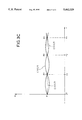
- FIG. 3C shows, as a function of the frequency f of the signal transmitted, attenuation curves A for three transmission lines of the same type and length in accordance with another embodiment of the invention.
- FIG. 3C shows the amplitude response of three transmission lines L1, L2 and L3 in the case where, for example, three reference frequencies are considered. The curves thus meet at three points: M1 at frequency f1, M2 at frequency f2 and M3 at frequency f3.
- the correction system according to the invention additionally makes it possible to provide a significant reduction in the spread between different lines and, secondly, to simplify adjustment by using analog delay line filters. It thus becomes possible to provide correction systems for several transmission lines in parallel. This can for example involve correcting the various transmission lines of a single multi-conductor cable.
- FIG. 4 shows one application of the correction system according to the invention in the case where, for example three transmission lines are put in parallel.
- Correction determination block or subassembly B1 is common to the three lines. It is supplied with respective amplitude and frequency reference values R1 and R2, the signal detection components (C1,D, C2) and the comparison components (1, 12) being incorporated into the subassembly.
- Each transmission line is fitted with a correction subassembly: subassembly B21 for line L1, B22 for line L2 and B23 for line L3.
- Each correction subassembly incorporates components for applying correction for frequency (7, 8, 9, 4, 10) together with devices for amplifying the signal (13, 2, 11).
Applications Claiming Priority (2)
| Application Number | Priority Date | Filing Date | Title |
|---|---|---|---|
| FR9116375 | 1991-12-31 | ||
| FR9116375A FR2685832B1 (fr) | 1991-12-31 | 1991-12-31 | Systeme correcteur de lignes de transmission. |
Publications (1)
| Publication Number | Publication Date |
|---|---|
| US5442328A true US5442328A (en) | 1995-08-15 |
Family
ID=9420696
Family Applications (1)
| Application Number | Title | Priority Date | Filing Date |
|---|---|---|---|
| US07/999,374 Expired - Lifetime US5442328A (en) | 1991-12-31 | 1992-12-31 | Transmission line correction system |
Country Status (4)
| Country | Link |
|---|---|
| US (1) | US5442328A (fr) |
| EP (1) | EP0550316B1 (fr) |
| DE (1) | DE69220022T2 (fr) |
| FR (1) | FR2685832B1 (fr) |
Cited By (4)
| Publication number | Priority date | Publication date | Assignee | Title |
|---|---|---|---|---|
| EP0767545A1 (fr) * | 1995-10-06 | 1997-04-09 | Plessey Semiconductors Limited | Egalisateur pour réseau local |
| GB2306068B (en) * | 1995-10-06 | 1999-07-07 | Plessey Semiconductors Ltd | LAN equalizer |
| EP1392001A1 (fr) * | 2002-08-22 | 2004-02-25 | Vrije Universiteit Brussel | Egaliseur adaptatif |
| US20050261880A1 (en) * | 2004-05-24 | 2005-11-24 | Gorin Joseph M | Noise compensation for spectrum analyzer |
Families Citing this family (2)
| Publication number | Priority date | Publication date | Assignee | Title |
|---|---|---|---|---|
| AU5084698A (en) * | 1996-10-11 | 1998-05-11 | Whitaker Corporation, The | Level control for a broadband distribution system |
| FR2946213B1 (fr) * | 2009-05-29 | 2012-05-11 | Sagem Comm | Procede de correction de la degradation du signal telephonique entrainee par la longueur de ligne analogique par le combine |
Citations (8)
| Publication number | Priority date | Publication date | Assignee | Title |
|---|---|---|---|---|
| US2794866A (en) * | 1953-03-28 | 1957-06-04 | Philips Corp | Device for the transmission of a video signal containing a direct-current component through a transmission cable |
| US3573667A (en) * | 1969-10-08 | 1971-04-06 | Bell Telephone Labor Inc | Automatic equalizer adjustment apparatus |
| US4151490A (en) * | 1977-03-21 | 1979-04-24 | Rca Corporation | Automatic cable equalizer circuit |
| JPS5552645A (en) * | 1978-10-14 | 1980-04-17 | Nec Corp | Automatic equalizer |
| US4250459A (en) * | 1978-03-10 | 1981-02-10 | Siemens Aktiengesellschaft | Circuit arrangement for automatic distortion correction of a signal |
| US4258340A (en) * | 1978-04-12 | 1981-03-24 | Nippon Electric Co., Ltd. | Amplitude equalizer |
| JPS61140233A (ja) * | 1984-12-12 | 1986-06-27 | Nec Corp | 伝送線路の低域損失補償方式 |
| US4984079A (en) * | 1989-07-26 | 1991-01-08 | Hughes Aircraft Company | Video preamplifier circuit |
-
1991
- 1991-12-31 FR FR9116375A patent/FR2685832B1/fr not_active Expired - Fee Related
-
1992
- 1992-12-21 EP EP92403487A patent/EP0550316B1/fr not_active Expired - Lifetime
- 1992-12-21 DE DE69220022T patent/DE69220022T2/de not_active Expired - Lifetime
- 1992-12-31 US US07/999,374 patent/US5442328A/en not_active Expired - Lifetime
Patent Citations (8)
| Publication number | Priority date | Publication date | Assignee | Title |
|---|---|---|---|---|
| US2794866A (en) * | 1953-03-28 | 1957-06-04 | Philips Corp | Device for the transmission of a video signal containing a direct-current component through a transmission cable |
| US3573667A (en) * | 1969-10-08 | 1971-04-06 | Bell Telephone Labor Inc | Automatic equalizer adjustment apparatus |
| US4151490A (en) * | 1977-03-21 | 1979-04-24 | Rca Corporation | Automatic cable equalizer circuit |
| US4250459A (en) * | 1978-03-10 | 1981-02-10 | Siemens Aktiengesellschaft | Circuit arrangement for automatic distortion correction of a signal |
| US4258340A (en) * | 1978-04-12 | 1981-03-24 | Nippon Electric Co., Ltd. | Amplitude equalizer |
| JPS5552645A (en) * | 1978-10-14 | 1980-04-17 | Nec Corp | Automatic equalizer |
| JPS61140233A (ja) * | 1984-12-12 | 1986-06-27 | Nec Corp | 伝送線路の低域損失補償方式 |
| US4984079A (en) * | 1989-07-26 | 1991-01-08 | Hughes Aircraft Company | Video preamplifier circuit |
Non-Patent Citations (4)
| Title |
|---|
| Patent Abstract of Japan vol. 10 No. 337 (E 454)(2393) Nov. 14, 1986 & JP A 61 140 233 (NEC) Jun. 27, 1986. * |
| Patent Abstract of Japan vol. 10 No. 337 (E-454)(2393) Nov. 14, 1986 & JP-A-61 140 233 (NEC) Jun. 27, 1986. |
| Patent Abstract of Japan vol. 4 No. 87 (E 16)(569) Jun. 21 1980 & JP A 55 052 645 (Nippon Denki) Apr. 17, 1980. * |
| Patent Abstract of Japan vol. 4 No. 87 (E-16)(569) Jun. 21 1980 & JP-A-55 052 645 (Nippon Denki) Apr. 17, 1980. |
Cited By (7)
| Publication number | Priority date | Publication date | Assignee | Title |
|---|---|---|---|---|
| EP0767545A1 (fr) * | 1995-10-06 | 1997-04-09 | Plessey Semiconductors Limited | Egalisateur pour réseau local |
| US5793264A (en) * | 1995-10-06 | 1998-08-11 | Plessey Semiconductor Limited | LAN equalizer |
| GB2306068B (en) * | 1995-10-06 | 1999-07-07 | Plessey Semiconductors Ltd | LAN equalizer |
| EP1392001A1 (fr) * | 2002-08-22 | 2004-02-25 | Vrije Universiteit Brussel | Egaliseur adaptatif |
| WO2004019512A1 (fr) * | 2002-08-22 | 2004-03-04 | Vrije Universiteit Brussel | Egaliseur adaptatif |
| US20060098727A1 (en) * | 2002-08-22 | 2006-05-11 | Vrije Universiteit Brussel | Adaptive equalizer |
| US20050261880A1 (en) * | 2004-05-24 | 2005-11-24 | Gorin Joseph M | Noise compensation for spectrum analyzer |
Also Published As
| Publication number | Publication date |
|---|---|
| DE69220022D1 (de) | 1997-07-03 |
| EP0550316A1 (fr) | 1993-07-07 |
| DE69220022T2 (de) | 1997-10-02 |
| FR2685832B1 (fr) | 1994-02-11 |
| EP0550316B1 (fr) | 1997-05-28 |
| FR2685832A1 (fr) | 1993-07-02 |
Similar Documents
| Publication | Publication Date | Title |
|---|---|---|
| EP0117654B2 (fr) | Amplificateur multi étage | |
| GB2164823A (en) | Television transmitter | |
| JPH0677858A (ja) | ケーブル減衰自動補償装置 | |
| US6492865B1 (en) | Band pass filter from two filters | |
| US6919774B2 (en) | Broadband PIN diode attenuator bias network | |
| US5442328A (en) | Transmission line correction system | |
| US4496859A (en) | Notch filter system | |
| EP0928063A2 (fr) | Amplificateur de télévision par cable à large bande passante à commande de pente et de gain par microprocesseur | |
| US4238766A (en) | Channel level adjusting apparatus | |
| US5789993A (en) | Amplitude/frequency correcting device and corresponding frequency equalizer | |
| US4450417A (en) | Feed forward circuit | |
| US5307031A (en) | Standard or reference transmission line with variable group time delay | |
| US3849744A (en) | Base-band delay equalizer | |
| US4225834A (en) | Equalizing network having a plurality of frequency sensitive attenuation branches in a negative feedback arrangement | |
| US4280102A (en) | Frequency response characteristic adjustable circuit | |
| US5910731A (en) | Front end interface circuit and method of tuning the same | |
| US4289928A (en) | Tone control arrangement for use in sound reproducing instruments | |
| US4403201A (en) | Bandpass filter circuit | |
| US4204176A (en) | Variable equalizer | |
| US4606043A (en) | Programmable automatic cable equalizer | |
| US4354160A (en) | Amplitude equalizer | |
| US4080580A (en) | Variable equalizer | |
| US4764938A (en) | Circuit and method for correcting distortion in a digital audio system | |
| US4127750A (en) | Apparatus for transmitting and receiving pulses | |
| US3774118A (en) | Line amplifier |
Legal Events
| Date | Code | Title | Description |
|---|---|---|---|
| AS | Assignment |
Owner name: THOMSON BROADCAST, FRANCE Free format text: ASSIGNMENT OF ASSIGNORS INTEREST;ASSIGNOR:HALIN, PIERRE;REEL/FRAME:007212/0769 Effective date: 19930302 |
|
| STCF | Information on status: patent grant |
Free format text: PATENTED CASE |
|
| FEPP | Fee payment procedure |
Free format text: PAYOR NUMBER ASSIGNED (ORIGINAL EVENT CODE: ASPN); ENTITY STATUS OF PATENT OWNER: LARGE ENTITY |
|
| FPAY | Fee payment |
Year of fee payment: 4 |
|
| FEPP | Fee payment procedure |
Free format text: PAYOR NUMBER ASSIGNED (ORIGINAL EVENT CODE: ASPN); ENTITY STATUS OF PATENT OWNER: LARGE ENTITY Free format text: PAYER NUMBER DE-ASSIGNED (ORIGINAL EVENT CODE: RMPN); ENTITY STATUS OF PATENT OWNER: LARGE ENTITY |
|
| FPAY | Fee payment |
Year of fee payment: 8 |
|
| FPAY | Fee payment |
Year of fee payment: 12 |