US5343419A - Analog calculation circuit using timers - Google Patents
Analog calculation circuit using timers Download PDFInfo
- Publication number
- US5343419A US5343419A US07/964,157 US96415792A US5343419A US 5343419 A US5343419 A US 5343419A US 96415792 A US96415792 A US 96415792A US 5343419 A US5343419 A US 5343419A
- Authority
- US
- United States
- Prior art keywords
- input
- circuit
- capacitance
- voltage
- resistance
- Prior art date
- Legal status (The legal status is an assumption and is not a legal conclusion. Google has not performed a legal analysis and makes no representation as to the accuracy of the status listed.)
- Expired - Fee Related
Links
Images


Classifications
-
- G—PHYSICS
- G06—COMPUTING OR CALCULATING; COUNTING
- G06G—ANALOGUE COMPUTERS
- G06G7/00—Devices in which the computing operation is performed by varying electric or magnetic quantities
- G06G7/12—Arrangements for performing computing operations, e.g. operational amplifiers specially adapted therefor
- G06G7/24—Arrangements for performing computing operations, e.g. operational amplifiers specially adapted therefor for evaluating logarithmic or exponential functions, e.g. hyperbolic functions
Definitions
- the present invention relates to a precise analog calculation circuit which utilizes timers.
- a digital calculation circuit is normally highly accurate but is usually rather large in scale.
- a typical analog calculation circuit performs rather imprecise calculations.
- a memory In a digital computer, a memory is used as a table for defining the relationship between an input and an output according to a mathematical calculation. This is merely one way to minimize the scale of the logical circuits required in order to perform a calculation.
- the memory itself is comprised of a large number of transistor gates and therefore, an immense amount of electrical power is wasted.
- An object of the present invention is to provide a calculation circuit which is small in scale but performs highly accurate calculations.
- a calculation circuit includes analog timers and produces an output voltage which is based on an exponential time factor.
- the present invention performs precise calculations because the exponential time factor, and can be produced by the use of conventional analog circuit technology.
- the circuit's physical scale is therefor much smaller than a conventional digital calculation circuit which performs a similar calculation.
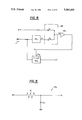
- FIG. 1 depicts a multiplication circuit according to one embodiment of the present invention.
- FIG. 2 is a diagram illustrating the characteristics of timers shown in FIG. 1.
- FIG. 3 shows a variation of the third timer of FIG. 1.
- FIG. 4 depicts a multiplication circuit according to another embodiment of the present invention.
- FIG. 5 shows another embodiment of a calculation circuit according to the present invention.
- FIG. 6 shows another embodiment of a calculation circuit according to the present invention.
- FIG. 7 is a diagram illustrating the characteristics of the embodiments shown in FIG. 4-6.
- FIG. 8 depicts an embodiment of an exponential calculation circuit according to the present invention.
- FIG. 9 shows the first RC circuit depicted in FIG.8.
- FIG. 10 shows a variation of the first RC circuit depicted in FIG. 8.
- FIG. 11 shows the second RC circuit depicted in FIG. 8.
- FIG. 12 shows a variation of the second RC circuit depicted in FIG. 8.
- FIG. 13 shows another variation of the second RC circuit depicted in FIG. 8.
- FIG. 14 shows another variation of the second RC circuit depicted in FIG. 8.
- FIG. 15 depicts another embodiment of an exponential circuit according to the present invention.
- FIG. 16 shows the first RC circuit depicted in FIG. 15.
- FIG. 17 shows a variation of the first RC circuit depicted in FIG. 15.
- FIG. 18 shows the second RC circuit depicted in FIG.15.
- FIG. 19 shows a variation of the second RC circuit depicted in FIG. 15.
- FIG. 20 shows another variation of the second RC circuit depicted in FIG. 15.
- FIG. 21 shows another variation of the second RC circuit depicted in FIG. 15.
- FIG. 22 depicts an embodiment of a subtraction circuit according to the present invention.
- FIG. 23 shows a variation of the third timer depicted in FIG. 22.
- FIG. 24 is a graph showing the relationship between time and the voltage at V 6 , V 3 and Z as seen in FIG. 22.
- the multiplication circuit comprises a first timer T 1 , a second timer T 2 and a third timer T 3 .
- Input voltage "X" and "Y” are input to timers T 1 and T 2 , respectively.
- Timer T 1 comprises capacitances C 1 and C 2 connected in series: the connection between capacitances C 1 and C 2 is grounded through a high resistance R 1 .
- a step voltage which acts as a starting trigger (ST) is input to the lead of capacitor C 1 which is not connected to capacitance C 2 .
- the input voltage "X” is connected through capacitance C 3 to capacitance C 2 .
- Inverter (INV 1 ) is connected between capacitances C 2 and C 3 .
- INV 1 outputs a maximum value when its input voltage is smaller than a threshold voltage, and it outputs 0V when its input voltage is above the threshold voltage.
- V st is the Maximal Voltage of the Starting Trigger ST
- Timer T 2 is constructed in a manner similar to timer T 1 .
- the construction elements are expressed using "'".
- the output of INV 1 is used as an input to capacitance C 1 '.
- the voltage between capacitance C 1 ' and capacitance C 2 ' begins to decrease and the output voltage of INV 1 ' becomes 0V when V 1 ' equals "Y".
- Timer T 3 comprises a pMOS ("Tr", hereafter) in which the output of INV 1 ' is used as the input to the gate of Tr.
- the starting trigger ST is input to the drain of Tr through capacitance C 4 and resistance R 2 .
- the source of Tr is grounded, Tr becomes conductive when the output voltage of INV 1 ' is above a threshold voltage.
- Tr When the gate voltage of Tr is 0V, a type of breaking occurs on Tr and the electrical charge of C 4 is maintained.
- timer T 3 is charged by starting trigger ST in period of time which is equal to the sum of the charging times for Timers T 1 and T 2 .
- the charging characteristic of timer T 3 can be expressed by the following equation: ##EQU2##
- t 3 is time
- V st is the Maximal Voltage of the Starting Trigger
- An RC circuit is very simple in structure as compared to digital multiplication circuits. Moreover, the voltage obtained according to the charging characteristic of an RC circuit is more precise than can be obtained by the use of general analog multiplication circuits.
- a multiplication circuit comprises timers T 1 , T 2 and T 3 .
- Input voltage "X” is input to timer T 1 and input voltage "Y” is input to timer T 2 .
- Timer T 1 comprises threshold element Th 1 which generates an output voltage when its input voltage is above a given threshold.
- Cp 1 which performs capacitive coupling of two inputs is connected to the input of Th 1 . If the voltage impressed upon capacitances C 1 and C 2 is V 1 and V 2 respectively, then the input voltage V 3 for Th 1 can be expressed by the following equation: ##EQU4##
- Th 1 comprises a pair of inverters INV 1 and INV 2 connected in series. When V 3 exceeds a threshold voltage, the output of INV 1 is 0V, and the output of INV 2 becomes high (i.e. the maximum voltage V m ).
- the first input voltage "X" is connected to capacitance C 1 , and a standard voltage pulse RP is connected to capacitance C 2 through resistance R 1 .
- Capacitance C 2 is grounded through capacitance "CC 1 ".
- FIG. 7 shows the change of V 1 and Vt 1 .
- Timer T 2 comprises threshold element Th 2 , capacitive coupling element Cp 2 , charging capacitance CC 2 and resistance R 2 .
- the construction of T 2 is similar to that of T 1 . Therefore, each element of T 2 corresponds to an element of T 1 : that is, Th 2 , Cp 2 , CC 2 and R 2 of T 2 corresponds to Th 1 , Cp 1 , CC 1 and R 1 of T 1 .
- the output of T 1 is the input to R 2 .
- Th 1 is at a maximal voltage V m
- capacitance CC 2 is charged and the input voltage V 4 to Cp 2 rises.
- Th 2 When V 5 exceeds the threshold voltage of Th 2 , Th 2 generates a maximum output voltage V m .
- Th 2 comprises three inverters INV 3 , INV 4 and INV 5 connected in series. The change in voltage at V 4 and Vt 2 is shown in FIG. 7. The period of time it takes Vt 2 to become 0V when Vt 1 becomes V m is labeled "ty". Therefore, the overall time it takes Vt 2 to reach 0V is tx+ty.
- T 3 comprises charging capacitance CC 3 .
- Voltage pulse RP is input to one terminal of capacitance CC 3 and the other lead is the output terminal Vt 3 .
- Vt 3 is grounded through resistance R 3 and an nMOS ("Th 3 ", hereafter)
- Vt 2 is input to the gate of Th 3 .
- CC 3 begins charging from the rise of voltage pulse RP and continues charging while Vt 2 is at the maximum voltage V m .
- Vt 2 becomes 0V at time tx+ty, a type of breaking occurs on Th 3 and the charging CC 3 is completed.
- Vt 3 can be expressed by the following formulas: ##EQU7##
- Vt 3 Vt 3
- X and Y can be obtained by the formula in (9).
- FIG. 5 shows a circuit of another embodiment of the present invention, in which timers T 4 and T 5 are used instead of timer T 3 in FIG. 4.
- Timer T 4 comprises nMOS Th 4 , charging capacitance CC 4 and resistance R 4 in the same way as was used in timer T 3 . ##EQU11##
- a predetermined value can be obtained by satisfying the relationship from the formula in (10).
- the output voltage Vt 4 can be expressed by the formula in (11). ##EQU12##
- the calculation in (11) is substantially the same as (XY) 1/2
- the calculation can be changed by changing the time constant.
- Timer T 5 has the same structure as timer T 4 , wherein only the time constant is changed. In this case the following formula is used:
- Vt 5 can then be expressed by the formula in (13) .
- timer T 6 is used instead of timer T 3 and timer T 6 comprises resistance R 6 , CMOS Th 6 and capacitance CC 6 in series. Furthermore, RP is connected to R 6 and CC 6 is grounded. The output terminal of timer T 6 is between Th 6 and CC 6 .
- the output Vt 6 of timer T 6 is described by the following formula: ##EQU14##
- Vt 6 can be expressed by the following formula: ##EQU15##
- the computation circuit comprises a first and second RC circuit to which a common standard voltage pulse RP is input.
- the capacitance of RC 1 and RC 2 is charged by RP in accordance with the time constant of the circuit.
- the output voltage V 1 of RC 1 is the input to one end of capacitance coupler CP and input voltage X is input to the another end of capacitance coupler CP.
- the output voltage V 2 of capacitance coupler CP can be expressed by the formula: ##EQU16##
- X and V 1 are linearly coupled. If capacitance C 1 is equal to capacitance C 2 , formula (16) can be expressed as: ##EQU17##
- the output voltage V 2 of capacitance coupler CP is input to threshold element Th 1 which outputs an output voltage "S" when V 2 reaches a predetermined voltage V th .
- RC 1 can be constructed as shown in FIG. 9 or in FIG. 10. In the structure shown in FIG. 9, one end of capacitance CC 1 is grounded and the other end is the output terminal to which RP is input through resistance R 1 . Expressing time as "t”, V 1 can be expressed as follows: ##EQU18## Thus, V 1 increases with time.
- FIG. 10 shows a structure similar to the structure in FIG. 9 with R 1 and CC 1 switched.
- Voltages V 1 and V 2 can be expressed by the formula: ##EQU20## Thus, both of these voltages decrease with time.
- threshold element Th 1 produces a corresponding output when the input is equal to or below a threshold voltage.
- RC 2 can be any of the structures shown in FIGS. 11-14. All of these comprise threshold element Th 2 , resistance R 2 and capacitance CC 2 .
- the circuit structures shown in FIG. 11 and 12 have the characteristic of increasing with time.
- Threshold element Th 2 performs a type of breaking between R 2 and CC 2 in FIG. 11, and between CC 2 and ground in FIG. 12.
- the output voltage Y of RC 2 depicted in FIG. 11 and 12 can be represented by the formula: ##EQU21##
- Threshold element Th 2 performs a type of breaking between R 2 and CC 2 in FIG. 13, and between CC 2 and ground in FIG. 14.
- the characteristic of these circuits can be expressed as: ##EQU22##
- Threshold element Th 1 generates an output when V 2 is equal to the threshold voltage V th , consequently, Th 2 performs a type of breaking and the voltage Y is preserved due to the fact that charging of capacitance CC 2 has stopped.
- the calculating circuit in this embodiment of the invention can perform exponential calculation on the input X with the exponent being equal to (R 1 CC 1 )/(R 2 CC 2 ).
- the characteristics of the circuit described by formulas (24) and (25) can be obtained from the relationship between RC 1 and RC 2 .
- the simple characteristics of the circuit described by formulas (26) and (27) can be obtained from the relationship between V th and RP.
- the computation circuit comprises a first and the second RC circuits RC 1 and RC 2 , respectively, to which a standard voltage pulse RP is input.
- the capacitance of RC 1 and RC 2 is charged by voltage pulse RP in accordance to its time constant.
- the output voltage V 1 of RC 1 is input to one terminal of capacitance coupler CP, input voltage X is input to another terminal of CP, and offset voltage V off is input to a third terminal of CP.
- the output voltage V 2 of CP is input to threshold element Th 1 which outputs an output voltage "S" when V 2 reaches the predetermined threshold voltage V th .
- RC 1 can have the construction as shown in FIG. 16 or in FIG. 17.
- one terminal of capacitance CC 1 is grounded and the other terminal is used as the output terminal to which voltage pulse RP is input through resistance R 1 .
- V 1 can be expressed by the following formula: ##EQU28##
- V 1 increases with time.
- formula (30) formula (29) can be rewritten as: ##EQU29## If the structure in FIG. 16 is used, threshold element Th 1 produces an output corresponding to the input when the input is over the threshold voltage.
- the circuit in FIG. 17 has the same type of structure used in FIG. 16 with only CC 1 and R 1 switched.
- V 1 and V 2 can be expressed by the formulas: ##EQU30## Thus, both of these voltages decrease with time. If the structure in FIG. 17 is used, threshold terminal Th 1 produces an output when the input is equal to or below the threshold voltage.
- RC 2 can be one of the structures shown in FIGS. 18-21, all of these embodiments comprise threshold element Th 2 resistance R 2 and capacitance CC 2 .
- the circuit structures shown in FIG. 18 and 19 have the characteristic of increasing with time.
- Threshold element Th 2 in FIG. 18 performs a type of breaking between R 2 and CC 2 .
- threshold element Th 2 performs a type of breaking between CC 2 and ground.
- the output voltage Y of RC 2 can be represented by the following formula, if the structures shown in FIG. 18 or 19 is used. ##EQU31##
- Threshold element Th 2 performs a type of breaking between R 2 and CC 2 .
- Th 2 performs a type of breaking between CC 2 and ground.
- the characteristic of these circuits can be expressed as in (35). ##EQU32##
- Th 1 generates an output when V 2 is equal to the threshold voltage V th , consequently, Th 2 performs a type of breaking and the voltage Y is preserved because the charging of CC 2 has stopped.
- the calculating circuit in this embodiment of the invention can perform exponential calculation on the input X with the exponent being (R 1 CC 1 )/(R 2 CC 2 ).
- the characteristics of the circuit expressed by formulas (36) and (37) can be obtained from the relationship between RC 1 and RC 2 .
- the characteristics of the circuit expressed by formulas (38) and (39) can be obtained from the relationship between V th and Rp.
- RP equals 3V th
- V off can be used in order to absorb any deviation in V th .
- a multiplication circuit comprises first, second and third times T 1 , T 2 and T 3 , respectively.
- Input voltage X is input to timer T 1
- input voltage Y is input to timer T 2 .
- Timer T 1 comprises threshold element Th 1 which generates an output voltage when its input voltage is over the threshold voltage.
- Capacity coupling Cp 1 is connected to the input of threshold element Th 1 .
- Capacity coupling Cp 1 comprises a pair of capacitances C 1 and C 2 connected in series.
- Threshold element Th 1 comprises a pair of inverters connected in series. When V 3 exceeds the threshold voltage, the output of INV 1 is 0V, and the output of INV 2 goes high (i.e. becomes its maximal voltage V m ).
- the first input voltage X is connected to C 1 .
- the standard voltage pulse RP is connected to C 2 through resistance R 1 .
- C 2 is grounded through charging capacitance C 3 . When RP goes high C 3 is charged and V 2 rises up to the same voltage level as RP.
- V 3 When RP rises up to a predetermined level and X is input to C 1 , C 3 is charged by a time constant which is determined by the value of C 3 xR 1 . Expressing time as "t”, V 3 can be expressed by the formula: ##EQU37## As seen by the expression in (41), V 3 rises as time increases. When V 3 exceeds the threshold voltage V th1 of Th 1 , the output voltage V 7 of Th 1 becomes the maximal voltage V m . The period of time it takes V 3 to rise from 0V to the threshold voltage V th1 is "tx". V th1 can then be represented by the formula: ##EQU38##
- Timer T 2 comprises threshold element Th 2 , a two input capacity coupling Cp 2 , charging capacitance C 6 and resistance R 2 . They are connected in a similar manner as its corresponding components in timer T 1 .
- Capacity coupling Cp 2 comprises a couple of capacitances C 4 and C 5 connected in series.
- Th 2 comprises a pair of inverters connected in series.
- V 6 exceeds the threshold voltage
- the output of INV 3 is 0V
- the output of INV 4 goes high (i.e. becomes the maximal voltage V m ).
- the second input voltage Y is connected to capacitance C 4 .
- the standard voltage pulse RP is connected to capacitance C 5 through resistance R 2 .
- Capacitance C 5 is grounded through charging capacitance C 6 .
- RP goes high, C 6 is charged and V 5 rises up to the same voltage level as RP.
- V 6 When RP rises up to the predetermined level and Y is input to capacitance C 4 , capacitance C 6 is charged by a time constant determined by the value of C 6 xR 2 . Expressing time as "t”, V 6 can be represented by the following formula: ##EQU40## As seen by formula (44), V 6 rises as time increases. When V 6 exceeds the threshold voltage V th2 of threshold element Th 2 , the output voltage V 8 of Th 2 becomes the maximal voltage V m . The time period it takes V 6 to rise from 0V to the threshold voltage V th2 is expressed by "ty", V th2 can then be represented by the following formula: ##EQU41##
- T 3 comprises charging capacitances C 7 .
- V 7 is input to one terminal of T 3 and the output voltage Z is measured at the other terminal.
- the output side of capacitance C 7 is grounded through resistance R 3 , and an nMOS ("Th 3 ", hereafter) V 8 is input to the gate of Th 3 .
- Capacitance C 7 is charged from the point that V 7 is V m , and it is completed at the point that V 8 is V m by the breaking of Th 3 . That is, capacitance C 7 is charged during the time period (ty-tx).
- FIG. 23 shows a timer T 4 comprising a resistance R 4 , a CMOS Th 4 and a capacitance C 8 in series instead of timer T 3 .
- Timer T 4 is connected to timer T 1 through resistance R 4 , C 8 is grounded, and timer T 2 is connected to the gate of the CMOS Th 4 .
- the output terminal of timer T 4 is located between Th 4 and C 8 .
- FIG. 24 is a set of graphs showing the voltages at V 3 , V 6 , and Z for the embodiment depicted in FIG. 22.
Landscapes
- Physics & Mathematics (AREA)
- Engineering & Computer Science (AREA)
- Mathematical Physics (AREA)
- Theoretical Computer Science (AREA)
- Software Systems (AREA)
- Computer Hardware Design (AREA)
- General Physics & Mathematics (AREA)
- Measurement Of Unknown Time Intervals (AREA)
Abstract
Description
R.sub.5 CC.sub.5 =2R.sub.1 CC.sub.1 =2R.sub.2 CC.sub.2 (12)
1-Z=V.sub.m (52)
Claims (26)
Applications Claiming Priority (10)
| Application Number | Priority Date | Filing Date | Title |
|---|---|---|---|
| JP4-280792 | 1992-09-25 | ||
| JP4280792A JP2985993B2 (en) | 1992-09-25 | 1992-09-25 | Multiplication circuit |
| JP4-292137 | 1992-10-06 | ||
| JP29213792A JP2850298B2 (en) | 1992-10-06 | 1992-10-06 | Multiplication circuit |
| JP4298110A JPH06119474A (en) | 1992-10-08 | 1992-10-08 | Arithmetic circuit |
| JP4-298110 | 1992-10-08 | ||
| JP4-298044 | 1992-10-09 | ||
| JP4298044A JP2972826B2 (en) | 1992-10-09 | 1992-10-09 | Arithmetic circuit |
| JP4304944A JP2845695B2 (en) | 1992-10-16 | 1992-10-16 | Division circuit |
| JP4-304944 | 1992-10-16 |
Publications (1)
| Publication Number | Publication Date |
|---|---|
| US5343419A true US5343419A (en) | 1994-08-30 |
Family
ID=27530680
Family Applications (1)
| Application Number | Title | Priority Date | Filing Date |
|---|---|---|---|
| US07/964,157 Expired - Fee Related US5343419A (en) | 1992-09-25 | 1992-10-21 | Analog calculation circuit using timers |
Country Status (1)
| Country | Link |
|---|---|
| US (1) | US5343419A (en) |
Cited By (2)
| Publication number | Priority date | Publication date | Assignee | Title |
|---|---|---|---|---|
| US5864495A (en) * | 1995-01-30 | 1999-01-26 | Canon Kabushiki Kaisha | Arithmetic processing apparatus and arithmetic processing circuit |
| US6134569A (en) * | 1997-01-30 | 2000-10-17 | Sharp Laboratories Of America, Inc. | Polyphase interpolator/decimator using continuous-valued, discrete-time signal processing |
Citations (2)
| Publication number | Priority date | Publication date | Assignee | Title |
|---|---|---|---|---|
| US3676661A (en) * | 1970-05-05 | 1972-07-11 | James A Sprowl | Voltage-time-voltage computation circuit using r-c exponential decay circuits to perform multiplication, division, root-finding and logarithmic conversion |
| US3831014A (en) * | 1973-02-02 | 1974-08-20 | Bailey Meter Co | Analog computer circuit for performing multiplication, division and square root |
-
1992
- 1992-10-21 US US07/964,157 patent/US5343419A/en not_active Expired - Fee Related
Patent Citations (2)
| Publication number | Priority date | Publication date | Assignee | Title |
|---|---|---|---|---|
| US3676661A (en) * | 1970-05-05 | 1972-07-11 | James A Sprowl | Voltage-time-voltage computation circuit using r-c exponential decay circuits to perform multiplication, division, root-finding and logarithmic conversion |
| US3831014A (en) * | 1973-02-02 | 1974-08-20 | Bailey Meter Co | Analog computer circuit for performing multiplication, division and square root |
Cited By (2)
| Publication number | Priority date | Publication date | Assignee | Title |
|---|---|---|---|---|
| US5864495A (en) * | 1995-01-30 | 1999-01-26 | Canon Kabushiki Kaisha | Arithmetic processing apparatus and arithmetic processing circuit |
| US6134569A (en) * | 1997-01-30 | 2000-10-17 | Sharp Laboratories Of America, Inc. | Polyphase interpolator/decimator using continuous-valued, discrete-time signal processing |
Similar Documents
| Publication | Publication Date | Title |
|---|---|---|
| US5490099A (en) | Method of multiplying an analog value by a digital value | |
| US6335654B1 (en) | Inrush current control circuit | |
| US5467039A (en) | Chip initialization signal generating circuit | |
| US20170205470A1 (en) | Brown out detector having sequential control function | |
| EP0858161B1 (en) | Delay circuit using pulse shaping | |
| JPH09180445A5 (en) | ||
| JP3005169B2 (en) | Reset circuit | |
| CA2172096A1 (en) | Adiabatic logic | |
| US5343419A (en) | Analog calculation circuit using timers | |
| GB2213668A (en) | A dual-slope waveform generation circuit | |
| JP2933112B2 (en) | Multiplication circuit | |
| KR20010024289A (en) | Zero power power-on-reset circuit | |
| WO1981001779A1 (en) | Switched-capacitor elliptic filter | |
| JPH0123003B2 (en) | ||
| US5929686A (en) | Semiconductor device with boot-strap output circuit and clamping circuit | |
| KR960039644A (en) | Evaluation method of signal propagation delay time of logic integrated circuit | |
| US3939413A (en) | Low cutoff digital pulse filter especially useful in electronic energy consumption meters | |
| US5196739A (en) | High voltage charge pump | |
| US5650752A (en) | Amplifier circuit with parallel connected amplifiers | |
| JPS584848B2 (en) | A/D conversion circuit | |
| JPS5842317A (en) | Analog-to-digital conversion circuit | |
| KR950007461B1 (en) | Pulse generator circuit for a certain period after power on | |
| JPH0426249B2 (en) | ||
| EP0772299A1 (en) | An interface circuit for controlling electronic switches with boosted voltage signals | |
| JPH0410807A (en) | Clock signal generating circuit |
Legal Events
| Date | Code | Title | Description |
|---|---|---|---|
| AS | Assignment |
Owner name: SHARP CORPORATION, JAPAN Free format text: ASSIGNMENT OF ASSIGNORS INTEREST;ASSIGNOR:YOZAN, INC.;REEL/FRAME:007430/0645 Effective date: 19950403 |
|
| FEPP | Fee payment procedure |
Free format text: PAYOR NUMBER ASSIGNED (ORIGINAL EVENT CODE: ASPN); ENTITY STATUS OF PATENT OWNER: LARGE ENTITY |
|
| FPAY | Fee payment |
Year of fee payment: 4 |
|
| FPAY | Fee payment |
Year of fee payment: 8 |
|
| AS | Assignment |
Owner name: YOZAN INC., JAPAN Free format text: ASSIGNMENT OF ASSIGNORS INTEREST;ASSIGNOR:YOZAN, INC. BY CHANGE OF NAME:TAKATORI EDUCATIONAL SOCIETY,INC.;REEL/FRAME:013552/0457 Effective date: 20021125 |
|
| REMI | Maintenance fee reminder mailed | ||
| LAPS | Lapse for failure to pay maintenance fees | ||
| STCH | Information on status: patent discontinuation |
Free format text: PATENT EXPIRED DUE TO NONPAYMENT OF MAINTENANCE FEES UNDER 37 CFR 1.362 |
|
| FP | Lapsed due to failure to pay maintenance fee |
Effective date: 20060830 |