US5250936A - Method for driving an independent sustain and address plasma display panel to prevent errant pixel erasures - Google Patents
Method for driving an independent sustain and address plasma display panel to prevent errant pixel erasures Download PDFInfo
- Publication number
- US5250936A US5250936A US07/512,880 US51288090A US5250936A US 5250936 A US5250936 A US 5250936A US 51288090 A US51288090 A US 51288090A US 5250936 A US5250936 A US 5250936A
- Authority
- US
- United States
- Prior art keywords
- sustain
- cell
- address
- lines
- cells
- Prior art date
- Legal status (The legal status is an assumption and is not a legal conclusion. Google has not performed a legal analysis and makes no representation as to the accuracy of the status listed.)
- Expired - Fee Related
Links
Images


Classifications
-
- G—PHYSICS
- G09—EDUCATION; CRYPTOGRAPHY; DISPLAY; ADVERTISING; SEALS
- G09G—ARRANGEMENTS OR CIRCUITS FOR CONTROL OF INDICATING DEVICES USING STATIC MEANS TO PRESENT VARIABLE INFORMATION
- G09G3/00—Control arrangements or circuits, of interest only in connection with visual indicators other than cathode-ray tubes
- G09G3/20—Control arrangements or circuits, of interest only in connection with visual indicators other than cathode-ray tubes for presentation of an assembly of a number of characters, e.g. a page, by composing the assembly by combination of individual elements arranged in a matrix no fixed position being assigned to or needed to be assigned to the individual characters or partial characters
- G09G3/22—Control arrangements or circuits, of interest only in connection with visual indicators other than cathode-ray tubes for presentation of an assembly of a number of characters, e.g. a page, by composing the assembly by combination of individual elements arranged in a matrix no fixed position being assigned to or needed to be assigned to the individual characters or partial characters using controlled light sources
- G09G3/28—Control arrangements or circuits, of interest only in connection with visual indicators other than cathode-ray tubes for presentation of an assembly of a number of characters, e.g. a page, by composing the assembly by combination of individual elements arranged in a matrix no fixed position being assigned to or needed to be assigned to the individual characters or partial characters using controlled light sources using luminous gas-discharge panels, e.g. plasma panels
- G09G3/288—Control arrangements or circuits, of interest only in connection with visual indicators other than cathode-ray tubes for presentation of an assembly of a number of characters, e.g. a page, by composing the assembly by combination of individual elements arranged in a matrix no fixed position being assigned to or needed to be assigned to the individual characters or partial characters using controlled light sources using luminous gas-discharge panels, e.g. plasma panels using AC panels
- G09G3/291—Control arrangements or circuits, of interest only in connection with visual indicators other than cathode-ray tubes for presentation of an assembly of a number of characters, e.g. a page, by composing the assembly by combination of individual elements arranged in a matrix no fixed position being assigned to or needed to be assigned to the individual characters or partial characters using controlled light sources using luminous gas-discharge panels, e.g. plasma panels using AC panels controlling the gas discharge to control a cell condition, e.g. by means of specific pulse shapes
- G09G3/292—Control arrangements or circuits, of interest only in connection with visual indicators other than cathode-ray tubes for presentation of an assembly of a number of characters, e.g. a page, by composing the assembly by combination of individual elements arranged in a matrix no fixed position being assigned to or needed to be assigned to the individual characters or partial characters using controlled light sources using luminous gas-discharge panels, e.g. plasma panels using AC panels controlling the gas discharge to control a cell condition, e.g. by means of specific pulse shapes for reset discharge, priming discharge or erase discharge occurring in a phase other than addressing
- G09G3/2927—Details of initialising
-
- G—PHYSICS
- G09—EDUCATION; CRYPTOGRAPHY; DISPLAY; ADVERTISING; SEALS
- G09G—ARRANGEMENTS OR CIRCUITS FOR CONTROL OF INDICATING DEVICES USING STATIC MEANS TO PRESENT VARIABLE INFORMATION
- G09G3/00—Control arrangements or circuits, of interest only in connection with visual indicators other than cathode-ray tubes
- G09G3/20—Control arrangements or circuits, of interest only in connection with visual indicators other than cathode-ray tubes for presentation of an assembly of a number of characters, e.g. a page, by composing the assembly by combination of individual elements arranged in a matrix no fixed position being assigned to or needed to be assigned to the individual characters or partial characters
- G09G3/22—Control arrangements or circuits, of interest only in connection with visual indicators other than cathode-ray tubes for presentation of an assembly of a number of characters, e.g. a page, by composing the assembly by combination of individual elements arranged in a matrix no fixed position being assigned to or needed to be assigned to the individual characters or partial characters using controlled light sources
- G09G3/28—Control arrangements or circuits, of interest only in connection with visual indicators other than cathode-ray tubes for presentation of an assembly of a number of characters, e.g. a page, by composing the assembly by combination of individual elements arranged in a matrix no fixed position being assigned to or needed to be assigned to the individual characters or partial characters using controlled light sources using luminous gas-discharge panels, e.g. plasma panels
- G09G3/288—Control arrangements or circuits, of interest only in connection with visual indicators other than cathode-ray tubes for presentation of an assembly of a number of characters, e.g. a page, by composing the assembly by combination of individual elements arranged in a matrix no fixed position being assigned to or needed to be assigned to the individual characters or partial characters using controlled light sources using luminous gas-discharge panels, e.g. plasma panels using AC panels
- G09G3/291—Control arrangements or circuits, of interest only in connection with visual indicators other than cathode-ray tubes for presentation of an assembly of a number of characters, e.g. a page, by composing the assembly by combination of individual elements arranged in a matrix no fixed position being assigned to or needed to be assigned to the individual characters or partial characters using controlled light sources using luminous gas-discharge panels, e.g. plasma panels using AC panels controlling the gas discharge to control a cell condition, e.g. by means of specific pulse shapes
- G09G3/293—Control arrangements or circuits, of interest only in connection with visual indicators other than cathode-ray tubes for presentation of an assembly of a number of characters, e.g. a page, by composing the assembly by combination of individual elements arranged in a matrix no fixed position being assigned to or needed to be assigned to the individual characters or partial characters using controlled light sources using luminous gas-discharge panels, e.g. plasma panels using AC panels controlling the gas discharge to control a cell condition, e.g. by means of specific pulse shapes for address discharge
-
- G—PHYSICS
- G09—EDUCATION; CRYPTOGRAPHY; DISPLAY; ADVERTISING; SEALS
- G09G—ARRANGEMENTS OR CIRCUITS FOR CONTROL OF INDICATING DEVICES USING STATIC MEANS TO PRESENT VARIABLE INFORMATION
- G09G3/00—Control arrangements or circuits, of interest only in connection with visual indicators other than cathode-ray tubes
- G09G3/20—Control arrangements or circuits, of interest only in connection with visual indicators other than cathode-ray tubes for presentation of an assembly of a number of characters, e.g. a page, by composing the assembly by combination of individual elements arranged in a matrix no fixed position being assigned to or needed to be assigned to the individual characters or partial characters
- G09G3/22—Control arrangements or circuits, of interest only in connection with visual indicators other than cathode-ray tubes for presentation of an assembly of a number of characters, e.g. a page, by composing the assembly by combination of individual elements arranged in a matrix no fixed position being assigned to or needed to be assigned to the individual characters or partial characters using controlled light sources
- G09G3/28—Control arrangements or circuits, of interest only in connection with visual indicators other than cathode-ray tubes for presentation of an assembly of a number of characters, e.g. a page, by composing the assembly by combination of individual elements arranged in a matrix no fixed position being assigned to or needed to be assigned to the individual characters or partial characters using controlled light sources using luminous gas-discharge panels, e.g. plasma panels
- G09G3/288—Control arrangements or circuits, of interest only in connection with visual indicators other than cathode-ray tubes for presentation of an assembly of a number of characters, e.g. a page, by composing the assembly by combination of individual elements arranged in a matrix no fixed position being assigned to or needed to be assigned to the individual characters or partial characters using controlled light sources using luminous gas-discharge panels, e.g. plasma panels using AC panels
- G09G3/291—Control arrangements or circuits, of interest only in connection with visual indicators other than cathode-ray tubes for presentation of an assembly of a number of characters, e.g. a page, by composing the assembly by combination of individual elements arranged in a matrix no fixed position being assigned to or needed to be assigned to the individual characters or partial characters using controlled light sources using luminous gas-discharge panels, e.g. plasma panels using AC panels controlling the gas discharge to control a cell condition, e.g. by means of specific pulse shapes
- G09G3/294—Control arrangements or circuits, of interest only in connection with visual indicators other than cathode-ray tubes for presentation of an assembly of a number of characters, e.g. a page, by composing the assembly by combination of individual elements arranged in a matrix no fixed position being assigned to or needed to be assigned to the individual characters or partial characters using controlled light sources using luminous gas-discharge panels, e.g. plasma panels using AC panels controlling the gas discharge to control a cell condition, e.g. by means of specific pulse shapes for lighting or sustain discharge
-
- G—PHYSICS
- G09—EDUCATION; CRYPTOGRAPHY; DISPLAY; ADVERTISING; SEALS
- G09G—ARRANGEMENTS OR CIRCUITS FOR CONTROL OF INDICATING DEVICES USING STATIC MEANS TO PRESENT VARIABLE INFORMATION
- G09G3/00—Control arrangements or circuits, of interest only in connection with visual indicators other than cathode-ray tubes
- G09G3/20—Control arrangements or circuits, of interest only in connection with visual indicators other than cathode-ray tubes for presentation of an assembly of a number of characters, e.g. a page, by composing the assembly by combination of individual elements arranged in a matrix no fixed position being assigned to or needed to be assigned to the individual characters or partial characters
- G09G3/22—Control arrangements or circuits, of interest only in connection with visual indicators other than cathode-ray tubes for presentation of an assembly of a number of characters, e.g. a page, by composing the assembly by combination of individual elements arranged in a matrix no fixed position being assigned to or needed to be assigned to the individual characters or partial characters using controlled light sources
- G09G3/28—Control arrangements or circuits, of interest only in connection with visual indicators other than cathode-ray tubes for presentation of an assembly of a number of characters, e.g. a page, by composing the assembly by combination of individual elements arranged in a matrix no fixed position being assigned to or needed to be assigned to the individual characters or partial characters using controlled light sources using luminous gas-discharge panels, e.g. plasma panels
- G09G3/288—Control arrangements or circuits, of interest only in connection with visual indicators other than cathode-ray tubes for presentation of an assembly of a number of characters, e.g. a page, by composing the assembly by combination of individual elements arranged in a matrix no fixed position being assigned to or needed to be assigned to the individual characters or partial characters using controlled light sources using luminous gas-discharge panels, e.g. plasma panels using AC panels
- G09G3/297—Control arrangements or circuits, of interest only in connection with visual indicators other than cathode-ray tubes for presentation of an assembly of a number of characters, e.g. a page, by composing the assembly by combination of individual elements arranged in a matrix no fixed position being assigned to or needed to be assigned to the individual characters or partial characters using controlled light sources using luminous gas-discharge panels, e.g. plasma panels using AC panels using opposed discharge type panels
-
- G—PHYSICS
- G09—EDUCATION; CRYPTOGRAPHY; DISPLAY; ADVERTISING; SEALS
- G09G—ARRANGEMENTS OR CIRCUITS FOR CONTROL OF INDICATING DEVICES USING STATIC MEANS TO PRESENT VARIABLE INFORMATION
- G09G3/00—Control arrangements or circuits, of interest only in connection with visual indicators other than cathode-ray tubes
- G09G3/20—Control arrangements or circuits, of interest only in connection with visual indicators other than cathode-ray tubes for presentation of an assembly of a number of characters, e.g. a page, by composing the assembly by combination of individual elements arranged in a matrix no fixed position being assigned to or needed to be assigned to the individual characters or partial characters
- G09G3/22—Control arrangements or circuits, of interest only in connection with visual indicators other than cathode-ray tubes for presentation of an assembly of a number of characters, e.g. a page, by composing the assembly by combination of individual elements arranged in a matrix no fixed position being assigned to or needed to be assigned to the individual characters or partial characters using controlled light sources
- G09G3/28—Control arrangements or circuits, of interest only in connection with visual indicators other than cathode-ray tubes for presentation of an assembly of a number of characters, e.g. a page, by composing the assembly by combination of individual elements arranged in a matrix no fixed position being assigned to or needed to be assigned to the individual characters or partial characters using controlled light sources using luminous gas-discharge panels, e.g. plasma panels
- G09G3/288—Control arrangements or circuits, of interest only in connection with visual indicators other than cathode-ray tubes for presentation of an assembly of a number of characters, e.g. a page, by composing the assembly by combination of individual elements arranged in a matrix no fixed position being assigned to or needed to be assigned to the individual characters or partial characters using controlled light sources using luminous gas-discharge panels, e.g. plasma panels using AC panels
- G09G3/298—Control arrangements or circuits, of interest only in connection with visual indicators other than cathode-ray tubes for presentation of an assembly of a number of characters, e.g. a page, by composing the assembly by combination of individual elements arranged in a matrix no fixed position being assigned to or needed to be assigned to the individual characters or partial characters using controlled light sources using luminous gas-discharge panels, e.g. plasma panels using AC panels using surface discharge panels
- G09G3/299—Control arrangements or circuits, of interest only in connection with visual indicators other than cathode-ray tubes for presentation of an assembly of a number of characters, e.g. a page, by composing the assembly by combination of individual elements arranged in a matrix no fixed position being assigned to or needed to be assigned to the individual characters or partial characters using controlled light sources using luminous gas-discharge panels, e.g. plasma panels using AC panels using surface discharge panels using alternate lighting of surface-type panels
-
- G—PHYSICS
- G09—EDUCATION; CRYPTOGRAPHY; DISPLAY; ADVERTISING; SEALS
- G09G—ARRANGEMENTS OR CIRCUITS FOR CONTROL OF INDICATING DEVICES USING STATIC MEANS TO PRESENT VARIABLE INFORMATION
- G09G3/00—Control arrangements or circuits, of interest only in connection with visual indicators other than cathode-ray tubes
- G09G3/20—Control arrangements or circuits, of interest only in connection with visual indicators other than cathode-ray tubes for presentation of an assembly of a number of characters, e.g. a page, by composing the assembly by combination of individual elements arranged in a matrix no fixed position being assigned to or needed to be assigned to the individual characters or partial characters
- G09G3/22—Control arrangements or circuits, of interest only in connection with visual indicators other than cathode-ray tubes for presentation of an assembly of a number of characters, e.g. a page, by composing the assembly by combination of individual elements arranged in a matrix no fixed position being assigned to or needed to be assigned to the individual characters or partial characters using controlled light sources
- G09G3/28—Control arrangements or circuits, of interest only in connection with visual indicators other than cathode-ray tubes for presentation of an assembly of a number of characters, e.g. a page, by composing the assembly by combination of individual elements arranged in a matrix no fixed position being assigned to or needed to be assigned to the individual characters or partial characters using controlled light sources using luminous gas-discharge panels, e.g. plasma panels
- G09G3/288—Control arrangements or circuits, of interest only in connection with visual indicators other than cathode-ray tubes for presentation of an assembly of a number of characters, e.g. a page, by composing the assembly by combination of individual elements arranged in a matrix no fixed position being assigned to or needed to be assigned to the individual characters or partial characters using controlled light sources using luminous gas-discharge panels, e.g. plasma panels using AC panels
- G09G3/298—Control arrangements or circuits, of interest only in connection with visual indicators other than cathode-ray tubes for presentation of an assembly of a number of characters, e.g. a page, by composing the assembly by combination of individual elements arranged in a matrix no fixed position being assigned to or needed to be assigned to the individual characters or partial characters using controlled light sources using luminous gas-discharge panels, e.g. plasma panels using AC panels using surface discharge panels
- G09G3/2983—Control arrangements or circuits, of interest only in connection with visual indicators other than cathode-ray tubes for presentation of an assembly of a number of characters, e.g. a page, by composing the assembly by combination of individual elements arranged in a matrix no fixed position being assigned to or needed to be assigned to the individual characters or partial characters using controlled light sources using luminous gas-discharge panels, e.g. plasma panels using AC panels using surface discharge panels using non-standard pixel electrode arrangements
- G09G3/2986—Control arrangements or circuits, of interest only in connection with visual indicators other than cathode-ray tubes for presentation of an assembly of a number of characters, e.g. a page, by composing the assembly by combination of individual elements arranged in a matrix no fixed position being assigned to or needed to be assigned to the individual characters or partial characters using controlled light sources using luminous gas-discharge panels, e.g. plasma panels using AC panels using surface discharge panels using non-standard pixel electrode arrangements with more than 3 electrodes involved in the operation
Definitions
- This invention relates to independent sustain and address AC plasma display panels, and more particularly to a method for preventing unwanted pixel erasures in such panels.
- A. C. Plasma display panels are well known in the art and, in general, comprise a pair of transparent substrates respectively supporting column and row electrodes, each coated with a dielectric layer and disposed in parallel spaced relation to define a gap therebetween in which an ionizable gas is sealed.
- the substrates are arranged such that the electrodes are disposed in orthogonal relation to one another thereby defining points of intersection which in turn define discharge cells at which selective discharges may be established to provide a desired storage or display function. It is also known to operate such panels with AC voltages and particularly to provide a write voltage which exceeds the firing voltage at a given discharge point, as defined by a selected column and row electrode, thereby to produce a discharge at a selected cell.
- the discharge at the selected cell can be continuously "sustained” by applying an alternating sustain voltage (which, by itself is insufficient to initiate a discharge).
- This technique relies upon the wall charges which are generated ON the dielectric layers of the substrates which, in conjunction with the sustain voltage, operate to maintain discharges.
- FIG. 1 an 8 ⁇ 8 pixel, independent sustain and address (hereinafter called "ISA") plasma panel schematic is shown.
- FIG. 2 shows an expanded view of the area in circle 10 in FIG. 1.
- the expanded view in FIG. 2 shows a basic nine cell group that is the repetitive unit in the ISA geometry.
- Each of the nine cells is defined in accordance with the types of electrodes that intersect to define a cell.
- all cells on the panel were electrically identical and, in fact, were all display pixels.
- P1, P2, P3, and P4 are display pixels i.e. P1, P2, P3, and P4.
- each cell group has four corresponding pixel cell types.
- each corresponding cell type e.g., P1, P2, etc.
- each cell group is subjected to identical sustain potentials during the operation of a panel, but its response to such potentials is controlled by potentials imposed on address lines which intersect each cell group.
- the cell group In addition to the four pixel cell types, there are five other cells in a cell group. At the center of the cell group is an address cell A which occurs at the intersection of two address electrodes XA and YA. There are also four coupling cells: C1, C2, C3, and C4 which occur at the intersections of a sustain electrode and an address electrode. The coupling cells are divided into two categories depending upon their position relative to the address cell. The C1 and C4 cells are called vertical coupling cells and the C2 and C3 cells are called horizontal coupling cells. It should be understood, that the terms vertical and horizontal are used merely to designate orthogonal orientations of conductors and cells and for easy reference purposes. No particular global orientation is to be implied therefrom.
- all horizontal electrodes of the ISA panel reside on one substrate of a panel and are referred to as the Y electrodes. All vertical electrodes reside on an opposite substrate and are termed X electrodes. As is well known, between the substrates, an ionizable gas is positioned and provides the selected cell illumination.
- the X address electrodes comprise electrodes 12, 14, 16 and 18 whereas the Y electrodes comprise 20, 22, 24, and 26. Each X electrode can be selectively addressed by a column address driver circuit 28 and each Y address line can be addressed by a row address driver circuit 30.
- X sustain signals are provided by two, phased, sustain generators 32 and 34, with each of the aforementioned sustain generators coupled to a connected pair of parallel sustain lines (e.g. 36, 38).
- Each pair of sustain lines, e.g. 36, 38, is shorted together by shorting bars at either end, thus forming a sustain electrode pair.
- Alternating sustain electrode pairs ON a given substrate are bussed together by a sustain bus and are connected to one of the two sustain drivers
- Row sustain drivers 40 and 42 are similarly connected to interspersed row sustain pairs.
- FIG. 3 waveforms are shown which describe a basic cycle for an ISA plasma panel as described in the aforementioned U.S. Pat. No. 4,772,884.
- two rows of pixel cells are initially turned ON.
- an erase cycle is performed to selectively turn off pixels which the image data indicate should be in the off state.
- the waveforms of FIG. 3 assume that a "write two rows" cycle has already occurred.
- the selective erase of certain desired ON pixels encompasses two steps. The first step causes a discharge to occur in selected address cells along a selected YA address electrode (see FIG. 2). This results in the migration of wall charges into vertical coupling cells C1 and C4.
- a reset pulse is applied to an address line to reset the wall voltages in vertical coupling cells C1 and C4 and address cell A.
- the simultaneous application of sustain voltages to XSa, XSb and YSa, YSb sustain lines with the reset pulses will cause small discharges to occur in the coupling cells which serve to adjust their wall voltages.
- Step 1 commences Step 1 of the selective erase procedure and its effect is shown in FIG. 4.
- the erase address waveforms are polarized so that the XA and YA electrodes are the anode and cathode respectively. Since the XA electrode is the anode, the plasma discharge 54, which occurs at address cell A, spreads predominantly towards vertical coupling cells C1 and C4. The voltage across the gaps in each of coupling cells C1 and C4 is such that the spreading plasma deposits significant negative charge into these cells.
- FIG. 5 a sectional illustration taken along line 5--5 in FIG. 4 (Step 1) is shown and illustrates the plasma spreading activity during Step 1 and the charges on the inner walls that are present at coupling cells C1 and C4 and address cell A.
- Step 2 of the selective erase address performs two degrees of selection. It commences at the fall of erase address pulses 50 and 52 and the rise of certain selection potentials on the sustain electrodes. As shown in FIG. 5, Step 1 deposited equal amounts of wall charge into coupling cells C1 and C4 when address cell A was discharged. By raising only the Y sustain line associated with a selected vertical coupling cell, the unselected vertical coupling cell, defined by the non-raised Y sustain line, will not discharge.
- Step 2 the selected YS and XA electrodes are the anode and cathode respectively. This polarization enables the plasma generated by the discharge of a coupling cell to spread horizontally away from the cell and into neighboring pixel cells. Sectional views taken along line 6--6 in FIG. 4 (Step 2) are shown in FIGS. 6a-6d and further aid in understanding the operation of the selective erase. In FIG. 3, the waveforms impressed on the X and Y sustain lines during Step 2 enable the selection of which of the pixel cells is to be erased.
- Step 1 it is assumed that Step 1 has already occurred; that coupling cell C1 has substantial wall charges which are polarized to provide a more positive voltage under the YSa electrode; and that both pixel cells P1 and P2 are in the ON state.
- 100 volt potentials are applied to the XSa and YSa electrodes respectively, and zero volts are placed on the XA and XSb electrodes.
- the stored wall charges in coupling cell C1 add to the applied potential on the YSa electrode to cause a discharge in cell C1.
- FIG. 6c a different set of initial conditions are assumed.
- cell P2 is in the off state and cell P1 is to be erased without affecting the state of cell P2. Since the dielectric immediately beneath the YSa electrode in cell P1 has a positive wall charge, the electrons resulting from a subsequent discharge of coupling cell C1 preferentially migrate thereto and neutralize the preexisting wall charge. Preexisting negative wall charges in pixel cell P2 tend to repel the electrons resulting from the discharge in coupling cell C1 and cell P2 remains unaffected.
- the sustain line that is raised during Step 2 of the selective erase determines the type of pixel cell that will be erased. Therefore, to erase a selected type of pixel cell, the two sustain electrodes that define the selected pixel cell type should rise simultaneously, following the fall of the XA address pulse.
- FIGS. 7a and 7b illustrate the problem in a non-addressed pixel group (i.e., any pixel group whose YA and XA address lines are not simultaneously pulsed), and show what happens during a Step 2 selective erase cycle in pixel cells that are of the same type as those in an addressed cell group.
- the problem is initiated by the sustain discharge that occurs (during a pixel P1 erase cycle) in unselected, but ON, pixel P2 during Step 2 of the erase cycle.
- the discharge of coupling cell Cl (caused by the application of a sustain pulse to the YSa electrode) causes electrons to spread along the YSa sustain line.
- pixel cell P2 is in the ON state, the spread of charge thereinto has no effect. It is to be remembered, however, that each cell group in the panel has like sustain pulses applied to like cell types, notwithstanding the non-addressed states of the cell groups in which those pixel types reside.
- FIG. 7a a non-addressed cell group is illustrated with both pixel cells P1 and P2 being in the ON state (wall voltages existing therein from a prior discharge).
- the indicated wall charges in coupling cell C1 indicate that the cell group was not selected during Step 1 of the erase cycle. Nevertheless, the wall charges within coupling cell C1 evidence the deposition of electrons (and resulting negative charges).
- sustain pulses are still applied to sustain lines XSa and YSa during the Step 2 erase cycle. Since these sustain potentials are applied throughout the panel to both addressed and non-addressed cells, their effects on non-addressed cells must be such as to not affect their cell states. This has been found not to be the case.
- a method for erasing pixel cells in an ISA AC plasma display panel comprises a plurality of cell groups aligned along horizontal and vertical dimensions, each cell group including an address cell, two vertical coupling cells, two horizontal coupling cells, and four pixel cells.
- Horizontal and vertical address lines are provided and intersect each address cell, and sustain lines are positioned on either side of the address lines and intersect adjacent series of pixel cells and coupling cells in each cell group. Intersections between sustain lines define pixel cells by type, with each cell group having identical first through fourth types at corresponding sustain line intersections.
- the method comprises: energizing the address and sustain lines line to turn ON at least a selected first type pixel cell in an addressed cell group, the first type pixel cell and a second type pixel cell defined by intersections between a horizontal sustain line and first and second vertical sustain lines; applying sustain signal pulses to all the sustain lines, with at least one less sustain signal pulse being applied to vertical sustain lines which define the second type pixel cell in all cell groups; and subsequently applying to the sustain lines, a sustain potential to cause erasure of the selected first type pixels in the addressed cell groups.
- FIG. 1 is an exemplary circuit diagram of a prior art ISA AC plasma panel.
- FIG. 2 is an expanded view of a cell group from FIG. 1.
- FIG. 3 shows a set of waveforms used to erase selected pixels in the AC plasma panel of FIG. 1.
- FIG. 4 illustrates the plasma spreading effects which occur during Step 1 and Step 2 of a selective erase cycle.
- FIG. 5 is a section taken along line 5--5 in FIG. 4 (Step 1).
- FIGS. 6a and 6b are sections taken along line 6--6 in FIG. 4 (Step 2), showing the operation of a Step 2 discharge to erase a P1 pixel cell while a P2 pixel cell is in the "ON" state.
- FIGS. 6c and 6d are sections taken along line 6--6 in FIG. 4 (Step 2), showing the operation of a Step 2 discharge to erase a P1 pixel cell while a P2 pixel cell is in the "off" state.
- FIGS. 7a and 7b are sections taken along the YSa sustain line in a non-addressed cell group, showing an errant erasure of pixel cell P1 which results from the discharge of pixel cell P2.
- FIG. 8 is a waveform diagram showing a set of waveforms which prevents the errant erasure shown in FIG. 7b.
- FIGS. 9a and 9b illustrate the application of the waveforms of FIG. 8 to an addressed cell group.
- FIG. 10 illustrates the effect of the waveforms of FIG. 8 upon a non-addressed cell group during the Step 2 erase procedure.
- FIG. 11 is a set of waveforms illustrating the waveforms required to restore a panel's brightness after a Step 2 erase cycle.
- FIG. 12 is a waveform diagram illustrating an alternative technique for restoring brightness to a panel after a Step 2 erase cycle.
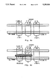
- FIG. 8 illustrates the potentials supplied to the X dimension address line XA; to Y dimension address line YA; and to sustain pair lines XSa, XSb, YSa, and YSb.
- Those waveforms illustrate a basic cycle which accomplishes the selective erase portion of pixel addressing in the panel. That erase cycle comprises two segments, i.e., Step 1 wherein a cell group is addressed and a coupling cell therein is caused to accumulate wall charges, and Step 2 wherein the wall charges within the coupling cell are caused to migrate into a selected pixel cell to cause erasure thereof.
- the selective erase commences with the application of erase address pulses 10 and 12 to the XA and YA lines respectively, to enable the addressing of an address cell in a selected cell group.
- a special sustain cycle occurs where a sustain pulse 14 is applied to the YSa and YSb sustain lines and is followed by a sustain pulse 16 applied to only one of the X dimension sustain lines.
- the non-pulsed X sustain line is the one that intersects the unselected pixel during the upcoming selective erase cycle. In other words, if the P1 pixel cell is to be erased, then no sustain pulse will be applied to the X dimension sustain line which intersects the P2 pixel cell.
- FIG. 9a From the charge states on coupling cell C1, it can be seen that it is prepared to be discharged during the up-coming application of a sustain pulse to the YSa electrode.
- the sustain pulse 16 (e.g., 100 volts) is applied to the XSa sustain line. That pulse causes pixel cell P1 to discharge and to reverse its wall charge state to that shown in FIG. 9a.
- the sustain pulse 16 e.g. 100 volts
- That pulse causes pixel cell P1 to discharge and to reverse its wall charge state to that shown in FIG. 9a.
- no sustain pulse is applied to the XSb sustain line at time A, and the wall charge state in P2 remains unchanged (as shown).
- the polarity of wall charges in the P2 pixel cell are exactly opposite those in the P1 pixel cell after time A. This is the condition which exists at the termination of sustain pulse 16 in FIG. 8.
- the subsequent application of address pulses 10 and 12 causes wall charges to be deposited in coupling cell C1, (FIG. 9a), thereby preparing the cell group for the Step 2 erase. That erase is accomplished by selectively applying a sustain pulse to the X and Y sustain lines which intersect the pixel to be erased. In this case, 100 volt pulses are applied to the XSa and YSa sustain lines. The sustain pulse on the YSa line causes coupling cell C1 to discharge. The electrons created by the C1 discharge migrate into pixel cell P1 and negate the positive wall charge state therein, thereby erasing the pixel. However, due to the fact that pixel cell P2 has an opposite polarity wall charge state to the sustain pulse on the YSa electrode, no discharge occurs therein.
- FIG. 10 cells (corresponding to those shown in FIGS. 9a and 9b) are illustrated for a non-addressed cell group.
- Coupling cell C1 has approximately equal charge states on both of its electrodes because no charge migration from an address cell has occurred.
- the wall charge states in pixel cells P1 and P2 exhibit opposite polarities. Since the wall charge polarity of P2 opposes the subsequently to-be-applied sustain pulse during Step 2, on YSa, a discharge is prevented within pixel cell P2 and no transfer of charge therefrom into P1 is possible.
- the XS sustain line that intersects the unselected pixel is not pulsed immediately preceding the selective erase cycle. That assures that the unselected pixel (and all identical type pixel cells elsewhere in the panel) will not discharge at Step 2 of the selective erase and cause errant erasures of unselected pixels of the same type as the pixel being erased in the addressed cell group.
- FIG. 11 A first preferred method for restoring the brightness is shown in FIG. 11 which, is in most respects identical to the waveform diagram of FIG. 8.
- an additional sustain pulse 20 is applied to the XS sustain line that intersects the unselected pixel.
- pulse 20 is applied to the XSb sustain line to discharge pixel cell P2 and cause its wall charge polarity to revert to that of pixel cell P1. (Note, Pixel cell P4 discharge at this time also.)
- FIG. 12 Another preferred method for restoring the brightness of the panel is shown in FIG. 12.
- Each erasure cycle is identical to that shown in FIG. 8.
- there needs to be two "sustain only" cycles each of which includes a pair of sustain pulses to cause the ON pixel cells in the panel to discharge, thereby restoring its brightness.
- this operation causes the reorientation of the wall charge polarity states in the unselected pixels automatically and without requiring any special extra pulse.
- a sustain pulse is not applied to pixel cells P2 during the P1 erase cycle.
- the special sustain cycle eliminates a sustain pulse from being applied to the P1 pixel cells.
- ON pixel cells P2 are caused to discharge and thus "catch up" with previously discharged ON P1 pixel cells, so that their wall charge polarities now match.
- Pulses 22 and 24 can be approximately one microsecond in length during Step 2 of the selective erase procedure. This reduction in time required to update the state of a pixel is of significant value and enables high image update requirements to be met. Thus, not only does this improve the driving method to remove a failure mode from the operation of an ISA plasma display panel, but it also provides the panel with an ability to perform faster image update procedures (useful when presenting grey scales and for panels with large numbers of pixels).
Landscapes
- Engineering & Computer Science (AREA)
- Physics & Mathematics (AREA)
- Power Engineering (AREA)
- Plasma & Fusion (AREA)
- Computer Hardware Design (AREA)
- General Physics & Mathematics (AREA)
- Theoretical Computer Science (AREA)
- Control Of Indicators Other Than Cathode Ray Tubes (AREA)
- Control Of Gas Discharge Display Tubes (AREA)
Abstract
Description
Claims (17)
Priority Applications (2)
| Application Number | Priority Date | Filing Date | Title |
|---|---|---|---|
| US07/512,880 US5250936A (en) | 1990-04-23 | 1990-04-23 | Method for driving an independent sustain and address plasma display panel to prevent errant pixel erasures |
| PCT/US1991/000695 WO1991016702A1 (en) | 1990-04-23 | 1991-02-01 | Method for driving an independent sustain and address plasma display panel to prevent errant pixel erasures |
Applications Claiming Priority (1)
| Application Number | Priority Date | Filing Date | Title |
|---|---|---|---|
| US07/512,880 US5250936A (en) | 1990-04-23 | 1990-04-23 | Method for driving an independent sustain and address plasma display panel to prevent errant pixel erasures |
Publications (1)
| Publication Number | Publication Date |
|---|---|
| US5250936A true US5250936A (en) | 1993-10-05 |
Family
ID=24040999
Family Applications (1)
| Application Number | Title | Priority Date | Filing Date |
|---|---|---|---|
| US07/512,880 Expired - Fee Related US5250936A (en) | 1990-04-23 | 1990-04-23 | Method for driving an independent sustain and address plasma display panel to prevent errant pixel erasures |
Country Status (2)
| Country | Link |
|---|---|
| US (1) | US5250936A (en) |
| WO (1) | WO1991016702A1 (en) |
Cited By (9)
| Publication number | Priority date | Publication date | Assignee | Title |
|---|---|---|---|---|
| US5663741A (en) * | 1993-04-30 | 1997-09-02 | Fujitsu Limited | Controller of plasma display panel and method of controlling the same |
| US5739798A (en) * | 1993-12-02 | 1998-04-14 | Central Research Laboratories Limited | Analogue greyscale addressing in a ferroelectric liquid crystal display with sub-electrode structure |
| US5739799A (en) * | 1995-07-05 | 1998-04-14 | Oki Electric Industry Co., Ltd. | Method of memory-driving a DC gaseous discharge panel and circuitry therefor |
| US5854540A (en) * | 1996-06-18 | 1998-12-29 | Mitsubishi Denki Kabushiki Kaisha | Plasma display panel driving method and plasma display panel device therefor |
| US20020011800A1 (en) * | 1999-08-17 | 2002-01-31 | Schermerhorn Jerry D. | Flat plasma display panel with independent trigger and controlled sustaining electrodes |
| US6400342B2 (en) * | 1997-12-05 | 2002-06-04 | Fujitsu Limited | Method of driving a plasma display panel before erase addressing |
| US6633269B2 (en) * | 2000-11-10 | 2003-10-14 | Au Optronics Corp. | Driving method for plasma display panels |
| US20060113921A1 (en) * | 1998-06-18 | 2006-06-01 | Noriaki Setoguchi | Method for driving plasma display panel |
| US7589697B1 (en) * | 1999-04-26 | 2009-09-15 | Imaging Systems Technology | Addressing of AC plasma display |
Families Citing this family (1)
| Publication number | Priority date | Publication date | Assignee | Title |
|---|---|---|---|---|
| AU2006200045B2 (en) * | 2000-09-14 | 2008-07-10 | Px Biosolutions Pty Ltd | Composition comprising immunogenic microparticles |
Citations (5)
| Publication number | Priority date | Publication date | Assignee | Title |
|---|---|---|---|---|
| US3559190A (en) * | 1966-01-18 | 1971-01-26 | Univ Illinois | Gaseous display and memory apparatus |
| US3906451A (en) * | 1974-04-15 | 1975-09-16 | Control Data Corp | Plasma panel erase apparatus |
| US4097780A (en) * | 1976-08-17 | 1978-06-27 | Bell Telephone Laboratories, Incorporated | Method and apparatus for energizing the cells of a plasma display panel to selected brightness levels |
| US4591847A (en) * | 1969-12-15 | 1986-05-27 | International Business Machines Corporation | Method and apparatus for gas display panel |
| US4772884A (en) * | 1985-10-15 | 1988-09-20 | University Patents, Inc. | Independent sustain and address plasma display panel |
-
1990
- 1990-04-23 US US07/512,880 patent/US5250936A/en not_active Expired - Fee Related
-
1991
- 1991-02-01 WO PCT/US1991/000695 patent/WO1991016702A1/en unknown
Patent Citations (5)
| Publication number | Priority date | Publication date | Assignee | Title |
|---|---|---|---|---|
| US3559190A (en) * | 1966-01-18 | 1971-01-26 | Univ Illinois | Gaseous display and memory apparatus |
| US4591847A (en) * | 1969-12-15 | 1986-05-27 | International Business Machines Corporation | Method and apparatus for gas display panel |
| US3906451A (en) * | 1974-04-15 | 1975-09-16 | Control Data Corp | Plasma panel erase apparatus |
| US4097780A (en) * | 1976-08-17 | 1978-06-27 | Bell Telephone Laboratories, Incorporated | Method and apparatus for energizing the cells of a plasma display panel to selected brightness levels |
| US4772884A (en) * | 1985-10-15 | 1988-09-20 | University Patents, Inc. | Independent sustain and address plasma display panel |
Cited By (11)
| Publication number | Priority date | Publication date | Assignee | Title |
|---|---|---|---|---|
| US5663741A (en) * | 1993-04-30 | 1997-09-02 | Fujitsu Limited | Controller of plasma display panel and method of controlling the same |
| US5739798A (en) * | 1993-12-02 | 1998-04-14 | Central Research Laboratories Limited | Analogue greyscale addressing in a ferroelectric liquid crystal display with sub-electrode structure |
| US5739799A (en) * | 1995-07-05 | 1998-04-14 | Oki Electric Industry Co., Ltd. | Method of memory-driving a DC gaseous discharge panel and circuitry therefor |
| US5854540A (en) * | 1996-06-18 | 1998-12-29 | Mitsubishi Denki Kabushiki Kaisha | Plasma display panel driving method and plasma display panel device therefor |
| US6400342B2 (en) * | 1997-12-05 | 2002-06-04 | Fujitsu Limited | Method of driving a plasma display panel before erase addressing |
| US20060113921A1 (en) * | 1998-06-18 | 2006-06-01 | Noriaki Setoguchi | Method for driving plasma display panel |
| US7825875B2 (en) * | 1998-06-18 | 2010-11-02 | Hitachi Plasma Patent Licensing Co., Ltd. | Method for driving plasma display panel |
| US7589697B1 (en) * | 1999-04-26 | 2009-09-15 | Imaging Systems Technology | Addressing of AC plasma display |
| US20020011800A1 (en) * | 1999-08-17 | 2002-01-31 | Schermerhorn Jerry D. | Flat plasma display panel with independent trigger and controlled sustaining electrodes |
| US6825606B2 (en) | 1999-08-17 | 2004-11-30 | Lg Electronics Inc. | Flat plasma display panel with independent trigger and controlled sustaining electrodes |
| US6633269B2 (en) * | 2000-11-10 | 2003-10-14 | Au Optronics Corp. | Driving method for plasma display panels |
Also Published As
| Publication number | Publication date |
|---|---|
| WO1991016702A1 (en) | 1991-10-31 |
Similar Documents
| Publication | Publication Date | Title |
|---|---|---|
| US6160529A (en) | Method of driving plasma display panel, and display apparatus using the same | |
| US4737687A (en) | Method for driving a gas discharge panel | |
| DE69629106T2 (en) | Method and device for controlling a plasma display device | |
| KR100263247B1 (en) | Plasma display panel and its driving method | |
| KR100751000B1 (en) | Method for driving a gas discharge panel | |
| US6294875B1 (en) | Method of driving AC plasma display panel | |
| US6608609B1 (en) | Method for driving plasma display panel | |
| JPH06314078A (en) | Device and method for driving display | |
| EP0160455B1 (en) | Driving a gas discharge display device | |
| US4683470A (en) | Video mode plasma panel display | |
| US6489939B1 (en) | Method for driving plasma display panel and apparatus for driving the same | |
| US5250936A (en) | Method for driving an independent sustain and address plasma display panel to prevent errant pixel erasures | |
| US5430458A (en) | System and method for eliminating flicker in displays addressed at low frame rates | |
| JP2001222956A (en) | Ac plasma display, its driver and driving method | |
| US5247288A (en) | High speed addressing method and apparatus for independent sustain and address plasma display panel | |
| JP3787713B2 (en) | Plasma display device | |
| US6356261B1 (en) | Method for addressing plasma display panel | |
| KR100331970B1 (en) | Display panel having microgrooves and method of operation | |
| JP3697338B2 (en) | Driving method of AC type plasma display panel | |
| JP2895397B2 (en) | Driving method of gas discharge type display device | |
| KR20060126104A (en) | Plasma display device and driving method thereof | |
| US20020067321A1 (en) | Plasma display panel and method of driving the same capable of providing high definition and high aperture ratio | |
| US6661395B2 (en) | Method and device to drive a plasma display | |
| KR100297700B1 (en) | Method for driving plasma display panel | |
| JP3013475B2 (en) | Driving method of plasma display panel |
Legal Events
| Date | Code | Title | Description |
|---|---|---|---|
| AS | Assignment |
Owner name: BOARD OF TRUSTEES OF THE UNIVERSITY OF ILLINOIS, I Free format text: ASSIGNMENT OF ASSIGNORS INTEREST.;ASSIGNOR:WEBER, LARRY F.;REEL/FRAME:005340/0264 Effective date: 19900420 Owner name: BOARD OF TRUSTEES OF THE UNIVERSITY OF ILLINOIS, I Free format text: ASSIGNMENT OF ASSIGNORS INTEREST.;ASSIGNORS:WARREN, KEVIN W.;WEBER, LARRY F.;REEL/FRAME:005340/0260 Effective date: 19900420 |
|
| CC | Certificate of correction | ||
| FEPP | Fee payment procedure |
Free format text: PAT HOLDER CLAIMS SMALL ENTITY STATUS - SMALL BUSINESS (ORIGINAL EVENT CODE: SM02); ENTITY STATUS OF PATENT OWNER: SMALL ENTITY |
|
| REMI | Maintenance fee reminder mailed | ||
| FPAY | Fee payment |
Year of fee payment: 4 |
|
| SULP | Surcharge for late payment | ||
| FP | Lapsed due to failure to pay maintenance fee |
Effective date: 19971008 |
|
| REMI | Maintenance fee reminder mailed | ||
| LAPS | Lapse for failure to pay maintenance fees | ||
| STCH | Information on status: patent discontinuation |
Free format text: PATENT EXPIRED DUE TO NONPAYMENT OF MAINTENANCE FEES UNDER 37 CFR 1.362 |
|
| FP | Lapsed due to failure to pay maintenance fee |
Effective date: 20011005 |