US5233309A - Programmable gain amplifier - Google Patents
Programmable gain amplifier Download PDFInfo
- Publication number
- US5233309A US5233309A US07/819,376 US81937692A US5233309A US 5233309 A US5233309 A US 5233309A US 81937692 A US81937692 A US 81937692A US 5233309 A US5233309 A US 5233309A
- Authority
- US
- United States
- Prior art keywords
- gain element
- gain
- output
- input
- receiving
- Prior art date
- Legal status (The legal status is an assumption and is not a legal conclusion. Google has not performed a legal analysis and makes no representation as to the accuracy of the status listed.)
- Expired - Lifetime
Links
Images

Classifications
-
- H—ELECTRICITY
- H03—ELECTRONIC CIRCUITRY
- H03G—CONTROL OF AMPLIFICATION
- H03G3/00—Gain control in amplifiers or frequency changers without distortion of the input signal
- H03G3/001—Digital control of analog signals
-
- H—ELECTRICITY
- H03—ELECTRONIC CIRCUITRY
- H03G—CONTROL OF AMPLIFICATION
- H03G1/00—Details of arrangements for controlling amplification
- H03G1/0005—Circuits characterised by the type of controlling devices operated by a controlling current or voltage signal
- H03G1/0088—Circuits characterised by the type of controlling devices operated by a controlling current or voltage signal using discontinuously variable devices, e.g. switch-operated
Definitions
- the present invention concerns programmable gain amplifiers. More particularly, the invention concerns programmable gain amplifiers having impedance selection networks allowing programmability.
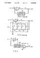
- FIG. 1 A conventional programmable gain amplifier (PGA) configuration is shown in FIG. 1.
- an amplifier 10 receives an input signal at an input 11 and provides an output signal, determined by the gain of the amplifier, at its output 12.
- the gain of amplifier 10 is determined by the impedance in the feedback path to the feedback input 13 is determined by an impedance selector 14 located in the feedback path between the output 12 and the feedback 13.
- the impedance selector may be, for instance, a variable resistor, or, as is often used in integrated circuits, a switch and resistor network.
- FIG. 2 A conventional programmable gain amplifier using a switch and resistor network as the impedance selector 14 is shown in FIG. 2.
- switches S 1 -S 4
- the input bias current flowing through the switches causes voltage variations due to a changing switch resistance with respect to the common-mode voltage. This non linear resistance variation results in non linear voltages biasing the input.
- CMOS complementary metal-oxide semiconductor
- a second switch may be used to offset variation in voltage caused by the first switch. This solution, however, increases both the noise caused by the switch and the die area of the integrated circuit.
- a programmable gain amplifier in accordance with the present invention includes first and second gain elements wherein the programmability of the gain of the amplifier is distributed over both gain elements.
- One embodiment of the present invention includes a first gain element having a first input, an output and at least one input for receiving a feedback signal, and a second gain element having at least one input and an output.
- An impedance having two leads, is connected in series between the feedback signal input and the input of the second gain element.
- a switch having two states, is connected in series with the output of the first gain element. In one state, the switch connects one lead of the impedance to the output of the first gain element. In the other state, the switch connects the other lead of the impedance to the output of the first gain element.
- Another embodiment of the present invention includes a first gain element having a first input, an output, and at least one input for receiving a feedback signal, and a feedback path for feeding back a signal from the output to the feedback signal input.
- a second gain element has at least one input and an output.
- At least one switch is connected in series with the output of the first gain element and has a first state wherein an impedance is placed in the feedback path, and a second state wherein an impedance is placed in series between the output of the first gain element and the input of the second gain element.
- Another embodiment in accordance with the invention includes a first gain element having a first input, an output, and at least one input for receiving a feedback signal, and a second gain element having at least a first input and an output.
- a plurality of series connected impedances, each having a first lead and a second lead are connected in series between the feedback signal input and the input of the second gain element.
- at least one corresponding switch is connected to receive the output of the first gain element and has a state for providing the received output to the first lead of the corresponding impedance.
- a first gain element having at least a first input, an output, and at least one input for receiving a feedback signal, and a feedback path for feeding back a signal from the output to the feedback signal input.
- a second gain element is provided and has at least a first input and an output.
- An impedance selection network is connected in series with the output of the first gain element and has at least two alternate states. In a first state, a first impedance is placed in the feedback path and a second impedance is placed in series between the output of the first gain element and the input of the second gain element. In a second state, a third impedance is placed in series between the output of the first gain element and the input of the second gain element and a fourth impedance is placed in the feedback path.
- a programmable gain amplifier according to the present invention may also be applied a differential (instrumentation amplifier) topology.
- Such an instrumentation amplifier is similar to a combination of two programmable gain amplifiers according to the invention which share a common second gain element which receives as its input the respective outputs of both of the first gain elements.
- Another advantage of the PGA in accordance with the invention is that the two separate gain elements permit the adjustment of two gains, and two bandwidths, which can be optimized for different applications. By placing most of the gain in the first element, noise performance may be optimized. By equalizing the gain between both stages, signal handling and bandwidth may be optimized.
- FIG. 1 is a block diagram of a conventional programmable gain amplifier
- FIG. 2 is a circuit diagram of an embodiment of a conventional programmable gain amplifier
- FIG. 3 is a block diagram of a programmable gain amplifier according to the present invention.
- FIG. 4 is a circuit diagram of an embodiment of a programmable gain amplifier in accordance with the present invention.
- FIG. 5 is a circuit diagram of a programmable gain instrumentation amplifier in accordance with the present invention.
- FIG. 3 A block diagram of a circuit embodying the present invention is shown in FIG. 3. It includes a first gain element 10 and second gain element 15 interconnected by an impedance selector 14B. In contrast to the conventional programmable gain amplifier, the impedance selector 14B is connected in series between the output 12 of the first gain element and the input 17 of a second gain element and allows variation of the gain of both elements.
- the impedance selector 14 includes a plurality of switches (S 1 -S n ) and corresponding impedances (R 1 -R n ).
- the switches are commonly connected to receive the output 12 of the first gain element.
- impedances R 1 -R n are shown as resistors for illustrative purposes. Other components providing an impedance may also be used and/or combined, such as capacitors.
- the PGA also includes, for the second gain element 15, a feedback resistor R c2 . Another resistor Rc 1 is provided between ground and the input of gain element 10. Resistor R c1 affects the gain of gain element 10.
- the invention is applicable to many other amplifier configurations and is not limited to those shown.
- the gain of the programmable gain amplifier in FIG. 4 depends on which switch is, or switches are, closed. For example, when switch S1 is closed, the gain of the amplifier is equal to -R c2 /(R1+R2+R3+Rn). If the sum of the impedances R1 through Rn is equal to R c2 , then the lowest gain is unity. If switch S2 is closed, the gain of the amplifier is (1+R1/R c1 ) * -R c2 /(R2+R3+Rn). The highest gain is obtained when switch Sn is closed. In this embodiment, that gain is (1+(R1+R2+R3)/R c1 ) * R c2 Rn. Given an arbitrary number N of switches S and corresponding resistors R, the gain G of the programmable amplifier of FIG. 2 when a single switch I is closed is equal to ##EQU1##
- the gain of the amplifier is distributed between the first and second stages.
- the first part of the product is the gain of the first stage.
- the second part of the product is the gain of the second stage. If the gain is equally divided between both stages, optimum bandwidth may be obtained. When most of the gain is obtained in the first stage, optimum noise performance may be obtained.
- all of the gain equations for the different states of the circuit are determined. These equations are solved as a simultaneous set to satisfy the desired conditions. For example, the circuit of FIG.
- R 4 may have most of the gain in the first stage by making R c1 have a low impedance compared to R 1 , R 2 , R 3 and (and their sums) and R c2 have a low impedance compared to R 1 , R 2 , R 3 , R N , and their sums.
- An effect of placing the impedance selector 14 in series between the output of the first gain element 10, and of dividing the programmability of gain over two gain elements is that the switches are not located in the signal path. That is, the switch noise is not fed back to the input 13 of the first gain element 10, but is attenuated by the open loop gain of the first gain element. The switch noise is not fed back because the effective output of the first gain element 10, which is received by the input of the second gain element 15, is the output of the switch S. Therefore, the switch is not in the feedback path of the first gain element 10.
- Another result of this configuration is that there is at least one resistor in the impedance selector which plays a dual role, i.e., it is part of the feedback path of first gain element 10 in one state; it is part of the input path of the second gain element 15 in another state.
- the present invention may also be applied to a differential (instrumentation amplifier) topology as shown in FIG. 3.
- the structure of the instrumentation amplifier is similar to the amplifier of FIG. 2 but also includes a third gain element 18 connected to the second gain element 15 via an impedance selector 19 in a manner similar to the connection of gain element 10 to gain element 15.
- the gain equations of this structure are generally the same as those described above.
- the programmable gain amplifier of the present invention is applicable to circuits having at least two cascaded gain elements.
- each gain element has a gain which is programmable by an impedance selector.
- a PGA in accordance with the present invention may be implemented using discrete components, such as on a printed circuit board, or in an integrated circuit, or even with vacuum tubes. It may also be implemented as a BiMOS integrated circuit in which the amplifiers are bipolar and the switches are CMOS.
Abstract
Description
Claims (14)
Priority Applications (6)
| Application Number | Priority Date | Filing Date | Title |
|---|---|---|---|
| US07/819,376 US5233309A (en) | 1992-01-09 | 1992-01-09 | Programmable gain amplifier |
| PCT/US1993/000162 WO1993014564A1 (en) | 1992-01-09 | 1993-01-08 | Programmable gain amplifier |
| JP05512591A JP3036843B2 (en) | 1992-01-09 | 1993-01-08 | Programmable gain amplifier |
| DE69306753T DE69306753T2 (en) | 1992-01-09 | 1993-01-08 | Programmable gain amplifier |
| EP93903033A EP0620955B1 (en) | 1992-01-09 | 1993-01-08 | Programmable gain amplifier |
| US08/011,106 US5486791A (en) | 1992-01-09 | 1993-01-29 | Programmable gain amplifier |
Applications Claiming Priority (1)
| Application Number | Priority Date | Filing Date | Title |
|---|---|---|---|
| US07/819,376 US5233309A (en) | 1992-01-09 | 1992-01-09 | Programmable gain amplifier |
Related Child Applications (1)
| Application Number | Title | Priority Date | Filing Date |
|---|---|---|---|
| US08/011,106 Continuation US5486791A (en) | 1992-01-09 | 1993-01-29 | Programmable gain amplifier |
Publications (1)
| Publication Number | Publication Date |
|---|---|
| US5233309A true US5233309A (en) | 1993-08-03 |
Family
ID=25227983
Family Applications (2)
| Application Number | Title | Priority Date | Filing Date |
|---|---|---|---|
| US07/819,376 Expired - Lifetime US5233309A (en) | 1992-01-09 | 1992-01-09 | Programmable gain amplifier |
| US08/011,106 Expired - Lifetime US5486791A (en) | 1992-01-09 | 1993-01-29 | Programmable gain amplifier |
Family Applications After (1)
| Application Number | Title | Priority Date | Filing Date |
|---|---|---|---|
| US08/011,106 Expired - Lifetime US5486791A (en) | 1992-01-09 | 1993-01-29 | Programmable gain amplifier |
Country Status (5)
| Country | Link |
|---|---|
| US (2) | US5233309A (en) |
| EP (1) | EP0620955B1 (en) |
| JP (1) | JP3036843B2 (en) |
| DE (1) | DE69306753T2 (en) |
| WO (1) | WO1993014564A1 (en) |
Cited By (43)
| Publication number | Priority date | Publication date | Assignee | Title |
|---|---|---|---|---|
| US5325071A (en) * | 1993-01-15 | 1994-06-28 | Texas Instruments Incorporated | Operational amplifier with digitally programmable gain circuitry on the same chip |
| US5523712A (en) * | 1994-03-09 | 1996-06-04 | Nippon Precision Circuits Inc. | Resistor array circuit device and variable gain device utilizing same |
| US5528181A (en) * | 1994-11-02 | 1996-06-18 | Advanced Micro Devices, Inc. | Hazard-free divider circuit |
| US5589830A (en) * | 1994-11-02 | 1996-12-31 | Advanced Micro Devices, Inc. | Stereo audio codec |
| US5675808A (en) * | 1994-11-02 | 1997-10-07 | Advanced Micro Devices, Inc. | Power control of circuit modules within an integrated circuit |
| US5794021A (en) * | 1994-11-02 | 1998-08-11 | Advanced Micro Devices, Inc. | Variable frequency clock generation circuit using aperiodic patterns |
| US5809466A (en) * | 1994-11-02 | 1998-09-15 | Advanced Micro Devices, Inc. | Audio processing chip with external serial port |
| US5923164A (en) * | 1996-10-15 | 1999-07-13 | Balluff, Inc. | Apparatus and method for automatically tuning the gain of an amplifier |
| US5946608A (en) * | 1996-09-30 | 1999-08-31 | Yamaha Corporation | Mixer circuit |
| US5999056A (en) * | 1998-06-30 | 1999-12-07 | Philips Electronics North Amercia Corporation | Variable gain amplifier using impedance network |
| US6104245A (en) * | 1996-03-28 | 2000-08-15 | Stichting Voor De Technische Wetenschappen | Measuring amplifier |
| US6272465B1 (en) | 1994-11-02 | 2001-08-07 | Legerity, Inc. | Monolithic PC audio circuit |
| US6288664B1 (en) | 1999-10-22 | 2001-09-11 | Eric J. Swanson | Autoranging analog to digital conversion circuitry |
| US6310518B1 (en) * | 1999-10-22 | 2001-10-30 | Eric J. Swanson | Programmable gain preamplifier |
| US20020082725A1 (en) * | 2000-07-25 | 2002-06-27 | Dute John C. | System, device and method for comprehensive input/output interface between process or machine transducers and controlling device or system |
| US6414619B1 (en) | 1999-10-22 | 2002-07-02 | Eric J. Swanson | Autoranging analog to digital conversion circuitry |
| US6448856B2 (en) * | 2000-02-04 | 2002-09-10 | Yamaha Corporation | Electronic volume circuit |
| US20030044027A1 (en) * | 2001-06-22 | 2003-03-06 | Yamaha Corporation | Volume circuit using resistive ladder circuits |
| US6538507B2 (en) * | 2001-02-28 | 2003-03-25 | Intersil Americas, Inc. | Automatic gain control circuit with high linearity and monotonically correlated offset voltage |
| WO2003049282A1 (en) * | 2001-11-29 | 2003-06-12 | Infineon Technologies Ag | Fully-differentiated differential amplifier with high input impedance |
| US6590517B1 (en) | 1999-10-22 | 2003-07-08 | Eric J. Swanson | Analog to digital conversion circuitry including backup conversion circuitry |
| US6646509B2 (en) * | 2002-01-23 | 2003-11-11 | Broadcom Corporation | Layout technique for matched resistors on an integrated circuit substrate |
| US6680652B2 (en) * | 2001-08-06 | 2004-01-20 | Rf Micro Devices, Inc. | Load switching for transmissions with different peak-to-average power ratios |
| US6693491B1 (en) * | 2000-04-17 | 2004-02-17 | Tripath Technology, Inc. | Method and apparatus for controlling an audio signal level |
| US20040121735A1 (en) * | 2002-12-23 | 2004-06-24 | James Tseng | Programmable gain amplifier with self-adjusting offset correction |
| US20040217815A1 (en) * | 2003-04-30 | 2004-11-04 | Canon Kabushiki Kaisha | Variable gain amplifier circuit using variable impedance circuit |
| US20040240918A1 (en) * | 2003-05-29 | 2004-12-02 | Manoj Soman | Gain or input volume controller and method utilizing a modified R2R ladder network |
| US20050035891A1 (en) * | 2003-08-14 | 2005-02-17 | Tripath Technology, Inc. | Digital-to-analog converter with level control |
| WO2005036733A2 (en) * | 2003-09-26 | 2005-04-21 | Austriamicrosystems Ag | Differential amplifier arrangement |
| GB2415844A (en) * | 2004-06-30 | 2006-01-04 | Renesas Tech Corp | Programmable gain amplifier with reduced gain switching transients |
| US20060038615A1 (en) * | 2004-08-17 | 2006-02-23 | National Instruments Corporation | Differential structure programmable gain instrumentation amplifier |
| US20060038614A1 (en) * | 2004-08-17 | 2006-02-23 | National Instruments Corporation | Programmable gain instrumentation amplifier with improved gain multiplexers |
| US20060119424A1 (en) * | 2004-12-03 | 2006-06-08 | Samsung Electro-Mechanics Co., Ltd. | Offset compensation circuit for a monitoring photodiode |
| US20080061873A1 (en) * | 2006-09-07 | 2008-03-13 | National Semiconductor Corporation | Gain Adjustment for Programmable Gain Amplifiers |
| US20090251215A1 (en) * | 2008-04-07 | 2009-10-08 | National Semiconductor Corporation | Amplifier output stage with extended operating range and reduced quiescent current |
| US20110068863A1 (en) * | 2009-08-14 | 2011-03-24 | That Corporation | Area Efficient, Programmable-Gain Amplifier |
| US20110163803A1 (en) * | 2010-01-06 | 2011-07-07 | Huimin Guo | Programmable Gain Amplifier and Embedded Filter |
| US8324969B2 (en) | 2011-03-11 | 2012-12-04 | Dialog Semiconductor Gmbh | Delta-sigma modulator approach to increased amplifier gain resolution |
| US20150084693A1 (en) * | 2013-09-20 | 2015-03-26 | Honeywell International Inc. | Programmable-gain instrumentation amplifier |
| US9143105B2 (en) | 2011-11-14 | 2015-09-22 | Dialog Semiconductor Gmbh | Sigma-delta modulator approach to increased volume resolution in audio output stages |
| US9692378B2 (en) | 2015-11-20 | 2017-06-27 | Texas Instruments Incorporated | Programmable gain amplifier with analog gain trim using interpolation |
| US10270407B2 (en) * | 2017-08-31 | 2019-04-23 | Core Chip Technology (Nanjing) Co., Ltd. | Programmable gain amplifier |
| US10419014B2 (en) * | 2018-02-06 | 2019-09-17 | Analog Devices, Inc. | Differential output PGIA architecture |
Families Citing this family (22)
| Publication number | Priority date | Publication date | Assignee | Title |
|---|---|---|---|---|
| US5621359A (en) * | 1995-07-27 | 1997-04-15 | Lucent Technologies Inc. | Gain selection technique |
| US5744944A (en) * | 1995-12-13 | 1998-04-28 | Sgs-Thomson Microelectronics, Inc. | Programmable bandwidth voltage regulator |
| US6259957B1 (en) * | 1997-04-04 | 2001-07-10 | Cirrus Logic, Inc. | Circuits and methods for implementing audio Codecs and systems using the same |
| US5987615A (en) * | 1997-12-22 | 1999-11-16 | Stmicroelectronics, Inc. | Programmable load transient compensator for reducing the transient response time to a load capable of operating at multiple power consumption levels |
| JP3653171B2 (en) * | 1998-03-09 | 2005-05-25 | 株式会社リコー | Variable gain amplifier |
| WO1999053613A1 (en) * | 1998-04-15 | 1999-10-21 | Ess Technology, Inc. | Attenuating volume control |
| US6486711B1 (en) | 1998-07-15 | 2002-11-26 | Texas Instruments Incorporated | Capacitor-based exponential programmable gain amplifier |
| US6239655B1 (en) * | 1999-04-08 | 2001-05-29 | Peavey Electronics Corporation | Microphone amplifier with digital gain control |
| US6541996B1 (en) * | 1999-12-21 | 2003-04-01 | Ati International Srl | Dynamic impedance compensation circuit and method |
| DE60107363T2 (en) * | 2000-02-14 | 2005-12-22 | Koninklijke Philips Electronics N.V. | CURRENT VOLTAGE TRANSFORMER WITH CONTROLLABLE GAIN AND SIGNAL PROCESSING CIRCUIT WITH SUCH A CONVERTER |
| US6833759B2 (en) * | 2002-01-23 | 2004-12-21 | Broadcom Corporation | System and method for a programmable gain amplifier |
| US6946910B2 (en) * | 2002-08-29 | 2005-09-20 | Agilent Technologies, Inc. | Configurable feedback path in an amplitude control system |
| TWI230503B (en) * | 2003-05-20 | 2005-04-01 | Mediatek Inc | Amplifier with fixed input impedance operated in various gain modes |
| US7391829B2 (en) * | 2003-07-02 | 2008-06-24 | Intel Corporation | Apparatus, system and method for receiver equalization |
| US7183855B2 (en) * | 2003-10-10 | 2007-02-27 | Siemens Aktiengesellschaft | Circuit arrangement for the switchable amplification of variable electrical signals |
| DE102004044741B4 (en) * | 2003-10-10 | 2007-04-19 | Siemens Ag | Circuit arrangement for switchable amplification of variable electrical signals |
| KR100783495B1 (en) | 2004-08-12 | 2007-12-11 | 인티그런트 테크놀로지즈(주) | Programmable Gain Control Amplifier |
| JP4335184B2 (en) * | 2004-08-12 | 2009-09-30 | インテグラント テクノロジーズ インコーポレーテッド | Highly linear programmable gain amplifier using switches |
| US8862253B2 (en) * | 2007-04-30 | 2014-10-14 | Sigmatel, Inc. | Gain control module and applications thereof |
| JP5089536B2 (en) * | 2008-09-10 | 2012-12-05 | 株式会社リコー | CURRENT LIMIT CIRCUIT AND CURRENT LIMIT CIRCUIT DRIVING METHOD |
| US9590579B2 (en) | 2014-10-07 | 2017-03-07 | Analog Devices, Inc. | Wide range transimpedance amplifier |
| US9966913B2 (en) | 2016-08-24 | 2018-05-08 | Hong Kong Applied Science and Technology Research Institute Company, Limited | Linear-in-dB, low-voltage, programmable/variable gain amplifier (PGA) using recursive current division |
Citations (3)
| Publication number | Priority date | Publication date | Assignee | Title |
|---|---|---|---|---|
| US3355670A (en) * | 1964-03-10 | 1967-11-28 | James J Pastoriza | High-speed switching apparatus |
| US4354159A (en) * | 1981-02-02 | 1982-10-12 | Rockwell International Corporation | Prescription attenuator having cascaded L-pad sections |
| US4396890A (en) * | 1979-05-09 | 1983-08-02 | Hitachi, Ltd. | Variable gain amplifier |
Family Cites Families (9)
| Publication number | Priority date | Publication date | Assignee | Title |
|---|---|---|---|---|
| US3579138A (en) * | 1969-08-25 | 1971-05-18 | American Optical Corp | Automatic gain presetting circuit |
| US4091333A (en) * | 1977-07-25 | 1978-05-23 | Valhalla Scientific Incorporated | Transconductance amplifier circuit |
| US4132957A (en) * | 1977-10-26 | 1979-01-02 | Hekimian Laboratories, Inc. | Programmable amplifier |
| DE3050495C1 (en) * | 1980-08-26 | 1984-04-12 | Mart Val'terovič Min | Step converter of electrical signals |
| US4523155A (en) * | 1983-05-04 | 1985-06-11 | Motorola, Inc. | Temperature compensated automatic output control circuitry for RF signal power amplifiers with wide dynamic range |
| DE3478730D1 (en) * | 1983-12-15 | 1989-07-20 | Matsushita Graphic Communic | Logarithmically linearly controlled variable gain amplifier |
| US4599574A (en) * | 1985-01-14 | 1986-07-08 | Neff Instrument Corporation | Selectable gain instrumentation amplifier |
| DE3731643A1 (en) * | 1987-09-19 | 1989-03-30 | Thomson Brandt Gmbh | CIRCUIT FOR THE LEVEL ADJUSTMENT OF AUDIO SIGNALS |
| GB8801750D0 (en) * | 1988-01-27 | 1988-02-24 | Gen Electric Co Plc | Gain control circuit |
-
1992
- 1992-01-09 US US07/819,376 patent/US5233309A/en not_active Expired - Lifetime
-
1993
- 1993-01-08 DE DE69306753T patent/DE69306753T2/en not_active Expired - Lifetime
- 1993-01-08 EP EP93903033A patent/EP0620955B1/en not_active Expired - Lifetime
- 1993-01-08 JP JP05512591A patent/JP3036843B2/en not_active Expired - Lifetime
- 1993-01-08 WO PCT/US1993/000162 patent/WO1993014564A1/en active IP Right Grant
- 1993-01-29 US US08/011,106 patent/US5486791A/en not_active Expired - Lifetime
Patent Citations (3)
| Publication number | Priority date | Publication date | Assignee | Title |
|---|---|---|---|---|
| US3355670A (en) * | 1964-03-10 | 1967-11-28 | James J Pastoriza | High-speed switching apparatus |
| US4396890A (en) * | 1979-05-09 | 1983-08-02 | Hitachi, Ltd. | Variable gain amplifier |
| US4354159A (en) * | 1981-02-02 | 1982-10-12 | Rockwell International Corporation | Prescription attenuator having cascaded L-pad sections |
Cited By (76)
| Publication number | Priority date | Publication date | Assignee | Title |
|---|---|---|---|---|
| US5325071A (en) * | 1993-01-15 | 1994-06-28 | Texas Instruments Incorporated | Operational amplifier with digitally programmable gain circuitry on the same chip |
| US5523712A (en) * | 1994-03-09 | 1996-06-04 | Nippon Precision Circuits Inc. | Resistor array circuit device and variable gain device utilizing same |
| US5794021A (en) * | 1994-11-02 | 1998-08-11 | Advanced Micro Devices, Inc. | Variable frequency clock generation circuit using aperiodic patterns |
| US5589830A (en) * | 1994-11-02 | 1996-12-31 | Advanced Micro Devices, Inc. | Stereo audio codec |
| US5648778A (en) * | 1994-11-02 | 1997-07-15 | Advanced Micro Devices, Inc. | Stereo audio CODEC |
| US5675808A (en) * | 1994-11-02 | 1997-10-07 | Advanced Micro Devices, Inc. | Power control of circuit modules within an integrated circuit |
| US5528181A (en) * | 1994-11-02 | 1996-06-18 | Advanced Micro Devices, Inc. | Hazard-free divider circuit |
| US5809466A (en) * | 1994-11-02 | 1998-09-15 | Advanced Micro Devices, Inc. | Audio processing chip with external serial port |
| US6272465B1 (en) | 1994-11-02 | 2001-08-07 | Legerity, Inc. | Monolithic PC audio circuit |
| US6104245A (en) * | 1996-03-28 | 2000-08-15 | Stichting Voor De Technische Wetenschappen | Measuring amplifier |
| US5946608A (en) * | 1996-09-30 | 1999-08-31 | Yamaha Corporation | Mixer circuit |
| US5923164A (en) * | 1996-10-15 | 1999-07-13 | Balluff, Inc. | Apparatus and method for automatically tuning the gain of an amplifier |
| US5999056A (en) * | 1998-06-30 | 1999-12-07 | Philips Electronics North Amercia Corporation | Variable gain amplifier using impedance network |
| US6310518B1 (en) * | 1999-10-22 | 2001-10-30 | Eric J. Swanson | Programmable gain preamplifier |
| US6590517B1 (en) | 1999-10-22 | 2003-07-08 | Eric J. Swanson | Analog to digital conversion circuitry including backup conversion circuitry |
| US6369740B1 (en) | 1999-10-22 | 2002-04-09 | Eric J. Swanson | Programmable gain preamplifier coupled to an analog to digital converter |
| US6288664B1 (en) | 1999-10-22 | 2001-09-11 | Eric J. Swanson | Autoranging analog to digital conversion circuitry |
| US6414619B1 (en) | 1999-10-22 | 2002-07-02 | Eric J. Swanson | Autoranging analog to digital conversion circuitry |
| US6452519B1 (en) * | 1999-10-22 | 2002-09-17 | Silicon Laboratories, Inc. | Analog to digital converter utilizing a highly stable resistor string |
| US6448856B2 (en) * | 2000-02-04 | 2002-09-10 | Yamaha Corporation | Electronic volume circuit |
| US6693491B1 (en) * | 2000-04-17 | 2004-02-17 | Tripath Technology, Inc. | Method and apparatus for controlling an audio signal level |
| US20020082725A1 (en) * | 2000-07-25 | 2002-06-27 | Dute John C. | System, device and method for comprehensive input/output interface between process or machine transducers and controlling device or system |
| US7912562B2 (en) | 2000-07-25 | 2011-03-22 | Electronic Solutions, Inc. | System, device and method for comprehensive input/output interface between process or machine transducers and controlling device or system |
| US7028105B2 (en) | 2000-07-25 | 2006-04-11 | Electronic Solutions, Inc. | Apparatus, method and signal set for monoline serial interface |
| US6538507B2 (en) * | 2001-02-28 | 2003-03-25 | Intersil Americas, Inc. | Automatic gain control circuit with high linearity and monotonically correlated offset voltage |
| US20030044027A1 (en) * | 2001-06-22 | 2003-03-06 | Yamaha Corporation | Volume circuit using resistive ladder circuits |
| US7298855B2 (en) * | 2001-06-22 | 2007-11-20 | Yamaha Corporation | Volume circuit using resistive ladder circuits |
| US6680652B2 (en) * | 2001-08-06 | 2004-01-20 | Rf Micro Devices, Inc. | Load switching for transmissions with different peak-to-average power ratios |
| WO2003049282A1 (en) * | 2001-11-29 | 2003-06-12 | Infineon Technologies Ag | Fully-differentiated differential amplifier with high input impedance |
| US6646509B2 (en) * | 2002-01-23 | 2003-11-11 | Broadcom Corporation | Layout technique for matched resistors on an integrated circuit substrate |
| USRE43776E1 (en) * | 2002-01-23 | 2012-10-30 | Broadcom Corporation | Layout technique for matched resistors on an integrated circuit substrate |
| US7157973B2 (en) | 2002-01-23 | 2007-01-02 | Broadcom Corporation | Layout technique for matched resistors on an integrated circuit substrate |
| US20040078771A1 (en) * | 2002-01-23 | 2004-04-22 | Sobel David A. | Layout technique for matched resistors on an integrated circuit substrate |
| US20050179497A1 (en) * | 2002-01-23 | 2005-08-18 | Broadcom Corporation | Layout technique for matched resistors on an integrated circuit substrate |
| US6958654B2 (en) | 2002-01-23 | 2005-10-25 | Broadcom Corporation | Layout technique for matched resistors on an integrated circuit substrate |
| US20040121735A1 (en) * | 2002-12-23 | 2004-06-24 | James Tseng | Programmable gain amplifier with self-adjusting offset correction |
| US7302246B2 (en) * | 2002-12-23 | 2007-11-27 | Intel Corporation | Programmable gain amplifier with self-adjusting offset correction |
| US20040217815A1 (en) * | 2003-04-30 | 2004-11-04 | Canon Kabushiki Kaisha | Variable gain amplifier circuit using variable impedance circuit |
| US6958655B2 (en) * | 2003-04-30 | 2005-10-25 | Canon Kabushiki Kaisha | Variable gain amplifier circuit using variable impedance circuit |
| US7162029B2 (en) | 2003-05-29 | 2007-01-09 | Cirrus Logic, Inc. | Gain or input volume controller and method utilizing a modified R2R ladder network |
| US20040240918A1 (en) * | 2003-05-29 | 2004-12-02 | Manoj Soman | Gain or input volume controller and method utilizing a modified R2R ladder network |
| US20050035891A1 (en) * | 2003-08-14 | 2005-02-17 | Tripath Technology, Inc. | Digital-to-analog converter with level control |
| WO2005036733A2 (en) * | 2003-09-26 | 2005-04-21 | Austriamicrosystems Ag | Differential amplifier arrangement |
| WO2005036733A3 (en) * | 2003-09-26 | 2009-03-05 | Austriamicrosystems Ag | Differential amplifier arrangement |
| US7327190B2 (en) | 2003-09-26 | 2008-02-05 | Austriamicrosystems Ag | Differential amplifier arrangement |
| US20070115047A1 (en) * | 2003-09-26 | 2007-05-24 | D Abramo Paolo | Differential amplifier arrangement |
| GB2415844B (en) * | 2004-06-30 | 2006-05-03 | Renesas Tech Corp | Wireless communication receiver |
| US20060128334A1 (en) * | 2004-06-30 | 2006-06-15 | Isao Ikuta | Wireless communication receiver |
| GB2415844A (en) * | 2004-06-30 | 2006-01-04 | Renesas Tech Corp | Programmable gain amplifier with reduced gain switching transients |
| US20060038615A1 (en) * | 2004-08-17 | 2006-02-23 | National Instruments Corporation | Differential structure programmable gain instrumentation amplifier |
| US7215197B2 (en) | 2004-08-17 | 2007-05-08 | National Instruments Corporation | Programmable gain instrumentation amplifier with improved gain multiplexers |
| US7327189B2 (en) | 2004-08-17 | 2008-02-05 | National Instruments Corporation | Differential structure programmable gain instrumentation amplifier |
| US20060038614A1 (en) * | 2004-08-17 | 2006-02-23 | National Instruments Corporation | Programmable gain instrumentation amplifier with improved gain multiplexers |
| US7209001B2 (en) * | 2004-12-03 | 2007-04-24 | Samsung Electro-Mechanics Co., Ltd. | Offset compensation circuit for a monitoring photodiode |
| CN100419445C (en) * | 2004-12-03 | 2008-09-17 | 三星电机株式会社 | Offset compensation circuit for a monitoring photodiode |
| US20060119424A1 (en) * | 2004-12-03 | 2006-06-08 | Samsung Electro-Mechanics Co., Ltd. | Offset compensation circuit for a monitoring photodiode |
| US20080061872A1 (en) * | 2006-09-07 | 2008-03-13 | National Semiconductor Corporation | Gain Adjustment for Programmable Gain Amplifiers |
| US7545209B2 (en) * | 2006-09-07 | 2009-06-09 | National Semiconductor Corporation | Gain adjustment for programmable gain amplifiers |
| US7545210B2 (en) * | 2006-09-07 | 2009-06-09 | National Semiconductor Corporation | Gain adjustment for programmable gain amplifiers |
| US7605659B2 (en) | 2006-09-07 | 2009-10-20 | National Semiconductor Corporation | Gain adjustment for programmable gain amplifiers |
| US20080252378A1 (en) * | 2006-09-07 | 2008-10-16 | National Semiconductor Corporation | Gain Adjustment for Programmable Gain Amplifiers |
| US20080061873A1 (en) * | 2006-09-07 | 2008-03-13 | National Semiconductor Corporation | Gain Adjustment for Programmable Gain Amplifiers |
| US20090251215A1 (en) * | 2008-04-07 | 2009-10-08 | National Semiconductor Corporation | Amplifier output stage with extended operating range and reduced quiescent current |
| US7920026B2 (en) | 2008-04-07 | 2011-04-05 | National Semiconductor Corporation | Amplifier output stage with extended operating range and reduced quiescent current |
| US20110068863A1 (en) * | 2009-08-14 | 2011-03-24 | That Corporation | Area Efficient, Programmable-Gain Amplifier |
| US8680920B2 (en) * | 2009-08-14 | 2014-03-25 | That Corporation | Area efficient, programmable-gain amplifier |
| TWI509987B (en) * | 2009-08-14 | 2015-11-21 | That Corp | Area efficient, programmable-gain amplifier |
| US8013672B2 (en) | 2010-01-06 | 2011-09-06 | Hong Kong Applied Science and Technology Research Institute Company Limited | Programmable gain amplifier and embedded filter |
| US20110163803A1 (en) * | 2010-01-06 | 2011-07-07 | Huimin Guo | Programmable Gain Amplifier and Embedded Filter |
| US8324969B2 (en) | 2011-03-11 | 2012-12-04 | Dialog Semiconductor Gmbh | Delta-sigma modulator approach to increased amplifier gain resolution |
| US9143105B2 (en) | 2011-11-14 | 2015-09-22 | Dialog Semiconductor Gmbh | Sigma-delta modulator approach to increased volume resolution in audio output stages |
| US20150084693A1 (en) * | 2013-09-20 | 2015-03-26 | Honeywell International Inc. | Programmable-gain instrumentation amplifier |
| US9065400B2 (en) * | 2013-09-20 | 2015-06-23 | Honeywell International Inc. | Programmable-gain instrumentation amplifier |
| US9692378B2 (en) | 2015-11-20 | 2017-06-27 | Texas Instruments Incorporated | Programmable gain amplifier with analog gain trim using interpolation |
| US10270407B2 (en) * | 2017-08-31 | 2019-04-23 | Core Chip Technology (Nanjing) Co., Ltd. | Programmable gain amplifier |
| US10419014B2 (en) * | 2018-02-06 | 2019-09-17 | Analog Devices, Inc. | Differential output PGIA architecture |
Also Published As
| Publication number | Publication date |
|---|---|
| JP3036843B2 (en) | 2000-04-24 |
| WO1993014564A1 (en) | 1993-07-22 |
| DE69306753T2 (en) | 1997-04-10 |
| US5486791A (en) | 1996-01-23 |
| JPH07508620A (en) | 1995-09-21 |
| EP0620955A1 (en) | 1994-10-26 |
| DE69306753D1 (en) | 1997-01-30 |
| EP0620955B1 (en) | 1996-12-18 |
Similar Documents
| Publication | Publication Date | Title |
|---|---|---|
| US5233309A (en) | Programmable gain amplifier | |
| US4855685A (en) | Precision switchable gain circuit | |
| US5523712A (en) | Resistor array circuit device and variable gain device utilizing same | |
| US6373337B1 (en) | Differential amplifier | |
| JP2532212B2 (en) | Variable attenuator | |
| CA1100201A (en) | Programmable attenuator apparatus employing active fet switching | |
| EP0474337A1 (en) | Switched low-loss attenuator | |
| US3684974A (en) | Automatic gain control rf-if amplifier | |
| US4467296A (en) | Integrated electronic controlled diode filter microwave networks | |
| US5708391A (en) | High frequency differential filter with CMOS control | |
| KR0151397B1 (en) | Ic filter and filter cell | |
| US4122417A (en) | Variable equalizer | |
| US6407627B1 (en) | Tunable sallen-key filter circuit assembly and method | |
| EP0834986B1 (en) | Gain control circuit and method | |
| EP0732807B1 (en) | Controllable filter arrangement | |
| EP0410295B1 (en) | Single-ended chopper stabilized operational amplifier | |
| US6876843B2 (en) | Radio frequency amplifier with improved intermodulation performance | |
| US4716321A (en) | Low noise, high thermal stability attenuator of the integratable type | |
| US4920325A (en) | Integrated active electronic switched capacitor filter having extremely low sensitivity to variations of the components | |
| US4609887A (en) | Delay equalizer | |
| US4540896A (en) | Variable resistance circuit | |
| GB2232029A (en) | D.c. blocking amplifiers | |
| US3983504A (en) | Active filter | |
| EP0589676B1 (en) | Variable voltage to current conversion circuit | |
| US3447091A (en) | Variable gain wide band bandpass amplifier |
Legal Events
| Date | Code | Title | Description |
|---|---|---|---|
| AS | Assignment |
Owner name: ANALOG DEVICES, INC., MASSACHUSETTS Free format text: ASSIGNMENT OF ASSIGNORS INTEREST.;ASSIGNORS:SPITALNY, PAUL;MALLINSON, MARTIN;REEL/FRAME:006055/0467 Effective date: 19920305 |
|
| FEPP | Fee payment procedure |
Free format text: PAYOR NUMBER ASSIGNED (ORIGINAL EVENT CODE: ASPN); ENTITY STATUS OF PATENT OWNER: LARGE ENTITY |
|
| STCF | Information on status: patent grant |
Free format text: PATENTED CASE |
|
| REMI | Maintenance fee reminder mailed | ||
| FPAY | Fee payment |
Year of fee payment: 4 |
|
| SULP | Surcharge for late payment | ||
| FEPP | Fee payment procedure |
Free format text: PAYER NUMBER DE-ASSIGNED (ORIGINAL EVENT CODE: RMPN); ENTITY STATUS OF PATENT OWNER: LARGE ENTITY Free format text: PAYOR NUMBER ASSIGNED (ORIGINAL EVENT CODE: ASPN); ENTITY STATUS OF PATENT OWNER: LARGE ENTITY |
|
| FEPP | Fee payment procedure |
Free format text: PAYER NUMBER DE-ASSIGNED (ORIGINAL EVENT CODE: RMPN); ENTITY STATUS OF PATENT OWNER: LARGE ENTITY Free format text: PAYOR NUMBER ASSIGNED (ORIGINAL EVENT CODE: ASPN); ENTITY STATUS OF PATENT OWNER: LARGE ENTITY |
|
| FPAY | Fee payment |
Year of fee payment: 8 |
|
| FPAY | Fee payment |
Year of fee payment: 12 |