US5043794A - Integrated circuit package and compact assemblies thereof - Google Patents
Integrated circuit package and compact assemblies thereof Download PDFInfo
- Publication number
- US5043794A US5043794A US07/587,308 US58730890A US5043794A US 5043794 A US5043794 A US 5043794A US 58730890 A US58730890 A US 58730890A US 5043794 A US5043794 A US 5043794A
- Authority
- US
- United States
- Prior art keywords
- integrated circuit
- assembly
- packages
- contact
- assemblies
- Prior art date
- Legal status (The legal status is an assumption and is not a legal conclusion. Google has not performed a legal analysis and makes no representation as to the accuracy of the status listed.)
- Expired - Lifetime
Links
Images


Classifications
-
- H—ELECTRICITY
- H01—ELECTRIC ELEMENTS
- H01L—SEMICONDUCTOR DEVICES NOT COVERED BY CLASS H10
- H01L23/00—Details of semiconductor or other solid state devices
- H01L23/34—Arrangements for cooling, heating, ventilating or temperature compensation ; Temperature sensing arrangements
- H01L23/36—Selection of materials, or shaping, to facilitate cooling or heating, e.g. heatsinks
- H01L23/367—Cooling facilitated by shape of device
- H01L23/3672—Foil-like cooling fins or heat sinks
-
- H—ELECTRICITY
- H01—ELECTRIC ELEMENTS
- H01L—SEMICONDUCTOR DEVICES NOT COVERED BY CLASS H10
- H01L23/00—Details of semiconductor or other solid state devices
- H01L23/12—Mountings, e.g. non-detachable insulating substrates
- H01L23/13—Mountings, e.g. non-detachable insulating substrates characterised by the shape
-
- H—ELECTRICITY
- H01—ELECTRIC ELEMENTS
- H01L—SEMICONDUCTOR DEVICES NOT COVERED BY CLASS H10
- H01L25/00—Assemblies consisting of a plurality of individual semiconductor or other solid state devices ; Multistep manufacturing processes thereof
- H01L25/03—Assemblies consisting of a plurality of individual semiconductor or other solid state devices ; Multistep manufacturing processes thereof all the devices being of a type provided for in the same subgroup of groups H01L27/00 - H01L33/00, or in a single subclass of H10K, H10N, e.g. assemblies of rectifier diodes
- H01L25/10—Assemblies consisting of a plurality of individual semiconductor or other solid state devices ; Multistep manufacturing processes thereof all the devices being of a type provided for in the same subgroup of groups H01L27/00 - H01L33/00, or in a single subclass of H10K, H10N, e.g. assemblies of rectifier diodes the devices having separate containers
- H01L25/105—Assemblies consisting of a plurality of individual semiconductor or other solid state devices ; Multistep manufacturing processes thereof all the devices being of a type provided for in the same subgroup of groups H01L27/00 - H01L33/00, or in a single subclass of H10K, H10N, e.g. assemblies of rectifier diodes the devices having separate containers the devices being of a type provided for in group H01L27/00
-
- H—ELECTRICITY
- H01—ELECTRIC ELEMENTS
- H01L—SEMICONDUCTOR DEVICES NOT COVERED BY CLASS H10
- H01L2224/00—Indexing scheme for arrangements for connecting or disconnecting semiconductor or solid-state bodies and methods related thereto as covered by H01L24/00
- H01L2224/01—Means for bonding being attached to, or being formed on, the surface to be connected, e.g. chip-to-package, die-attach, "first-level" interconnects; Manufacturing methods related thereto
- H01L2224/42—Wire connectors; Manufacturing methods related thereto
- H01L2224/44—Structure, shape, material or disposition of the wire connectors prior to the connecting process
- H01L2224/45—Structure, shape, material or disposition of the wire connectors prior to the connecting process of an individual wire connector
- H01L2224/45001—Core members of the connector
- H01L2224/45099—Material
- H01L2224/451—Material with a principal constituent of the material being a metal or a metalloid, e.g. boron (B), silicon (Si), germanium (Ge), arsenic (As), antimony (Sb), tellurium (Te) and polonium (Po), and alloys thereof
- H01L2224/45138—Material with a principal constituent of the material being a metal or a metalloid, e.g. boron (B), silicon (Si), germanium (Ge), arsenic (As), antimony (Sb), tellurium (Te) and polonium (Po), and alloys thereof the principal constituent melting at a temperature of greater than or equal to 950°C and less than 1550°C
- H01L2224/45144—Gold (Au) as principal constituent
-
- H—ELECTRICITY
- H01—ELECTRIC ELEMENTS
- H01L—SEMICONDUCTOR DEVICES NOT COVERED BY CLASS H10
- H01L2224/00—Indexing scheme for arrangements for connecting or disconnecting semiconductor or solid-state bodies and methods related thereto as covered by H01L24/00
- H01L2224/01—Means for bonding being attached to, or being formed on, the surface to be connected, e.g. chip-to-package, die-attach, "first-level" interconnects; Manufacturing methods related thereto
- H01L2224/42—Wire connectors; Manufacturing methods related thereto
- H01L2224/47—Structure, shape, material or disposition of the wire connectors after the connecting process
- H01L2224/48—Structure, shape, material or disposition of the wire connectors after the connecting process of an individual wire connector
- H01L2224/4805—Shape
- H01L2224/4809—Loop shape
- H01L2224/48091—Arched
-
- H—ELECTRICITY
- H01—ELECTRIC ELEMENTS
- H01L—SEMICONDUCTOR DEVICES NOT COVERED BY CLASS H10
- H01L2224/00—Indexing scheme for arrangements for connecting or disconnecting semiconductor or solid-state bodies and methods related thereto as covered by H01L24/00
- H01L2224/01—Means for bonding being attached to, or being formed on, the surface to be connected, e.g. chip-to-package, die-attach, "first-level" interconnects; Manufacturing methods related thereto
- H01L2224/42—Wire connectors; Manufacturing methods related thereto
- H01L2224/47—Structure, shape, material or disposition of the wire connectors after the connecting process
- H01L2224/48—Structure, shape, material or disposition of the wire connectors after the connecting process of an individual wire connector
- H01L2224/481—Disposition
- H01L2224/48151—Connecting between a semiconductor or solid-state body and an item not being a semiconductor or solid-state body, e.g. chip-to-substrate, chip-to-passive
- H01L2224/48221—Connecting between a semiconductor or solid-state body and an item not being a semiconductor or solid-state body, e.g. chip-to-substrate, chip-to-passive the body and the item being stacked
- H01L2224/48225—Connecting between a semiconductor or solid-state body and an item not being a semiconductor or solid-state body, e.g. chip-to-substrate, chip-to-passive the body and the item being stacked the item being non-metallic, e.g. insulating substrate with or without metallisation
- H01L2224/48227—Connecting between a semiconductor or solid-state body and an item not being a semiconductor or solid-state body, e.g. chip-to-substrate, chip-to-passive the body and the item being stacked the item being non-metallic, e.g. insulating substrate with or without metallisation connecting the wire to a bond pad of the item
-
- H—ELECTRICITY
- H01—ELECTRIC ELEMENTS
- H01L—SEMICONDUCTOR DEVICES NOT COVERED BY CLASS H10
- H01L2224/00—Indexing scheme for arrangements for connecting or disconnecting semiconductor or solid-state bodies and methods related thereto as covered by H01L24/00
- H01L2224/01—Means for bonding being attached to, or being formed on, the surface to be connected, e.g. chip-to-package, die-attach, "first-level" interconnects; Manufacturing methods related thereto
- H01L2224/42—Wire connectors; Manufacturing methods related thereto
- H01L2224/47—Structure, shape, material or disposition of the wire connectors after the connecting process
- H01L2224/48—Structure, shape, material or disposition of the wire connectors after the connecting process of an individual wire connector
- H01L2224/484—Connecting portions
- H01L2224/48463—Connecting portions the connecting portion on the bonding area of the semiconductor or solid-state body being a ball bond
- H01L2224/48464—Connecting portions the connecting portion on the bonding area of the semiconductor or solid-state body being a ball bond the other connecting portion not on the bonding area also being a ball bond, i.e. ball-to-ball
-
- H—ELECTRICITY
- H01—ELECTRIC ELEMENTS
- H01L—SEMICONDUCTOR DEVICES NOT COVERED BY CLASS H10
- H01L2224/00—Indexing scheme for arrangements for connecting or disconnecting semiconductor or solid-state bodies and methods related thereto as covered by H01L24/00
- H01L2224/01—Means for bonding being attached to, or being formed on, the surface to be connected, e.g. chip-to-package, die-attach, "first-level" interconnects; Manufacturing methods related thereto
- H01L2224/42—Wire connectors; Manufacturing methods related thereto
- H01L2224/47—Structure, shape, material or disposition of the wire connectors after the connecting process
- H01L2224/49—Structure, shape, material or disposition of the wire connectors after the connecting process of a plurality of wire connectors
- H01L2224/491—Disposition
- H01L2224/49105—Connecting at different heights
- H01L2224/49109—Connecting at different heights outside the semiconductor or solid-state body
-
- H—ELECTRICITY
- H01—ELECTRIC ELEMENTS
- H01L—SEMICONDUCTOR DEVICES NOT COVERED BY CLASS H10
- H01L2225/00—Details relating to assemblies covered by the group H01L25/00 but not provided for in its subgroups
- H01L2225/03—All the devices being of a type provided for in the same subgroup of groups H01L27/00 - H01L33/648 and H10K99/00
- H01L2225/10—All the devices being of a type provided for in the same subgroup of groups H01L27/00 - H01L33/648 and H10K99/00 the devices having separate containers
- H01L2225/1005—All the devices being of a type provided for in the same subgroup of groups H01L27/00 - H01L33/648 and H10K99/00 the devices having separate containers the devices being of a type provided for in group H01L27/00
- H01L2225/1011—All the devices being of a type provided for in the same subgroup of groups H01L27/00 - H01L33/648 and H10K99/00 the devices having separate containers the devices being of a type provided for in group H01L27/00 the containers being in a stacked arrangement
- H01L2225/1017—All the devices being of a type provided for in the same subgroup of groups H01L27/00 - H01L33/648 and H10K99/00 the devices having separate containers the devices being of a type provided for in group H01L27/00 the containers being in a stacked arrangement the lowermost container comprising a device support
- H01L2225/1035—All the devices being of a type provided for in the same subgroup of groups H01L27/00 - H01L33/648 and H10K99/00 the devices having separate containers the devices being of a type provided for in group H01L27/00 the containers being in a stacked arrangement the lowermost container comprising a device support the device being entirely enclosed by the support, e.g. high-density interconnect [HDI]
-
- H—ELECTRICITY
- H01—ELECTRIC ELEMENTS
- H01L—SEMICONDUCTOR DEVICES NOT COVERED BY CLASS H10
- H01L2225/00—Details relating to assemblies covered by the group H01L25/00 but not provided for in its subgroups
- H01L2225/03—All the devices being of a type provided for in the same subgroup of groups H01L27/00 - H01L33/648 and H10K99/00
- H01L2225/10—All the devices being of a type provided for in the same subgroup of groups H01L27/00 - H01L33/648 and H10K99/00 the devices having separate containers
- H01L2225/1005—All the devices being of a type provided for in the same subgroup of groups H01L27/00 - H01L33/648 and H10K99/00 the devices having separate containers the devices being of a type provided for in group H01L27/00
- H01L2225/1011—All the devices being of a type provided for in the same subgroup of groups H01L27/00 - H01L33/648 and H10K99/00 the devices having separate containers the devices being of a type provided for in group H01L27/00 the containers being in a stacked arrangement
- H01L2225/1047—Details of electrical connections between containers
- H01L2225/1064—Electrical connections provided on a side surface of one or more of the containers
-
- H—ELECTRICITY
- H01—ELECTRIC ELEMENTS
- H01L—SEMICONDUCTOR DEVICES NOT COVERED BY CLASS H10
- H01L2225/00—Details relating to assemblies covered by the group H01L25/00 but not provided for in its subgroups
- H01L2225/03—All the devices being of a type provided for in the same subgroup of groups H01L27/00 - H01L33/648 and H10K99/00
- H01L2225/10—All the devices being of a type provided for in the same subgroup of groups H01L27/00 - H01L33/648 and H10K99/00 the devices having separate containers
- H01L2225/1005—All the devices being of a type provided for in the same subgroup of groups H01L27/00 - H01L33/648 and H10K99/00 the devices having separate containers the devices being of a type provided for in group H01L27/00
- H01L2225/1011—All the devices being of a type provided for in the same subgroup of groups H01L27/00 - H01L33/648 and H10K99/00 the devices having separate containers the devices being of a type provided for in group H01L27/00 the containers being in a stacked arrangement
- H01L2225/1094—Thermal management, e.g. cooling
-
- H—ELECTRICITY
- H01—ELECTRIC ELEMENTS
- H01L—SEMICONDUCTOR DEVICES NOT COVERED BY CLASS H10
- H01L24/00—Arrangements for connecting or disconnecting semiconductor or solid-state bodies; Methods or apparatus related thereto
- H01L24/01—Means for bonding being attached to, or being formed on, the surface to be connected, e.g. chip-to-package, die-attach, "first-level" interconnects; Manufacturing methods related thereto
- H01L24/42—Wire connectors; Manufacturing methods related thereto
- H01L24/44—Structure, shape, material or disposition of the wire connectors prior to the connecting process
- H01L24/45—Structure, shape, material or disposition of the wire connectors prior to the connecting process of an individual wire connector
-
- H—ELECTRICITY
- H01—ELECTRIC ELEMENTS
- H01L—SEMICONDUCTOR DEVICES NOT COVERED BY CLASS H10
- H01L24/00—Arrangements for connecting or disconnecting semiconductor or solid-state bodies; Methods or apparatus related thereto
- H01L24/01—Means for bonding being attached to, or being formed on, the surface to be connected, e.g. chip-to-package, die-attach, "first-level" interconnects; Manufacturing methods related thereto
- H01L24/42—Wire connectors; Manufacturing methods related thereto
- H01L24/47—Structure, shape, material or disposition of the wire connectors after the connecting process
- H01L24/48—Structure, shape, material or disposition of the wire connectors after the connecting process of an individual wire connector
-
- H—ELECTRICITY
- H01—ELECTRIC ELEMENTS
- H01L—SEMICONDUCTOR DEVICES NOT COVERED BY CLASS H10
- H01L24/00—Arrangements for connecting or disconnecting semiconductor or solid-state bodies; Methods or apparatus related thereto
- H01L24/01—Means for bonding being attached to, or being formed on, the surface to be connected, e.g. chip-to-package, die-attach, "first-level" interconnects; Manufacturing methods related thereto
- H01L24/42—Wire connectors; Manufacturing methods related thereto
- H01L24/47—Structure, shape, material or disposition of the wire connectors after the connecting process
- H01L24/49—Structure, shape, material or disposition of the wire connectors after the connecting process of a plurality of wire connectors
-
- H—ELECTRICITY
- H01—ELECTRIC ELEMENTS
- H01L—SEMICONDUCTOR DEVICES NOT COVERED BY CLASS H10
- H01L2924/00—Indexing scheme for arrangements or methods for connecting or disconnecting semiconductor or solid-state bodies as covered by H01L24/00
- H01L2924/0001—Technical content checked by a classifier
- H01L2924/00014—Technical content checked by a classifier the subject-matter covered by the group, the symbol of which is combined with the symbol of this group, being disclosed without further technical details
-
- H—ELECTRICITY
- H01—ELECTRIC ELEMENTS
- H01L—SEMICONDUCTOR DEVICES NOT COVERED BY CLASS H10
- H01L2924/00—Indexing scheme for arrangements or methods for connecting or disconnecting semiconductor or solid-state bodies as covered by H01L24/00
- H01L2924/01—Chemical elements
- H01L2924/01013—Aluminum [Al]
-
- H—ELECTRICITY
- H01—ELECTRIC ELEMENTS
- H01L—SEMICONDUCTOR DEVICES NOT COVERED BY CLASS H10
- H01L2924/00—Indexing scheme for arrangements or methods for connecting or disconnecting semiconductor or solid-state bodies as covered by H01L24/00
- H01L2924/01—Chemical elements
- H01L2924/01029—Copper [Cu]
-
- H—ELECTRICITY
- H01—ELECTRIC ELEMENTS
- H01L—SEMICONDUCTOR DEVICES NOT COVERED BY CLASS H10
- H01L2924/00—Indexing scheme for arrangements or methods for connecting or disconnecting semiconductor or solid-state bodies as covered by H01L24/00
- H01L2924/01—Chemical elements
- H01L2924/01066—Dysprosium [Dy]
-
- H—ELECTRICITY
- H01—ELECTRIC ELEMENTS
- H01L—SEMICONDUCTOR DEVICES NOT COVERED BY CLASS H10
- H01L2924/00—Indexing scheme for arrangements or methods for connecting or disconnecting semiconductor or solid-state bodies as covered by H01L24/00
- H01L2924/01—Chemical elements
- H01L2924/01079—Gold [Au]
-
- H—ELECTRICITY
- H01—ELECTRIC ELEMENTS
- H01L—SEMICONDUCTOR DEVICES NOT COVERED BY CLASS H10
- H01L2924/00—Indexing scheme for arrangements or methods for connecting or disconnecting semiconductor or solid-state bodies as covered by H01L24/00
- H01L2924/095—Indexing scheme for arrangements or methods for connecting or disconnecting semiconductor or solid-state bodies as covered by H01L24/00 with a principal constituent of the material being a combination of two or more materials provided in the groups H01L2924/013 - H01L2924/0715
- H01L2924/097—Glass-ceramics, e.g. devitrified glass
- H01L2924/09701—Low temperature co-fired ceramic [LTCC]
-
- H—ELECTRICITY
- H01—ELECTRIC ELEMENTS
- H01L—SEMICONDUCTOR DEVICES NOT COVERED BY CLASS H10
- H01L2924/00—Indexing scheme for arrangements or methods for connecting or disconnecting semiconductor or solid-state bodies as covered by H01L24/00
- H01L2924/10—Details of semiconductor or other solid state devices to be connected
- H01L2924/11—Device type
- H01L2924/12—Passive devices, e.g. 2 terminal devices
- H01L2924/1203—Rectifying Diode
- H01L2924/12033—Gunn diode
-
- H—ELECTRICITY
- H01—ELECTRIC ELEMENTS
- H01L—SEMICONDUCTOR DEVICES NOT COVERED BY CLASS H10
- H01L2924/00—Indexing scheme for arrangements or methods for connecting or disconnecting semiconductor or solid-state bodies as covered by H01L24/00
- H01L2924/10—Details of semiconductor or other solid state devices to be connected
- H01L2924/11—Device type
- H01L2924/14—Integrated circuits
-
- H—ELECTRICITY
- H01—ELECTRIC ELEMENTS
- H01L—SEMICONDUCTOR DEVICES NOT COVERED BY CLASS H10
- H01L2924/00—Indexing scheme for arrangements or methods for connecting or disconnecting semiconductor or solid-state bodies as covered by H01L24/00
- H01L2924/15—Details of package parts other than the semiconductor or other solid state devices to be connected
- H01L2924/151—Die mounting substrate
- H01L2924/1515—Shape
- H01L2924/15153—Shape the die mounting substrate comprising a recess for hosting the device
- H01L2924/15155—Shape the die mounting substrate comprising a recess for hosting the device the shape of the recess being other than a cuboid
- H01L2924/15156—Side view
-
- H—ELECTRICITY
- H01—ELECTRIC ELEMENTS
- H01L—SEMICONDUCTOR DEVICES NOT COVERED BY CLASS H10
- H01L2924/00—Indexing scheme for arrangements or methods for connecting or disconnecting semiconductor or solid-state bodies as covered by H01L24/00
- H01L2924/15—Details of package parts other than the semiconductor or other solid state devices to be connected
- H01L2924/151—Die mounting substrate
- H01L2924/153—Connection portion
- H01L2924/1532—Connection portion the connection portion being formed on the die mounting surface of the substrate
-
- H—ELECTRICITY
- H01—ELECTRIC ELEMENTS
- H01L—SEMICONDUCTOR DEVICES NOT COVERED BY CLASS H10
- H01L2924/00—Indexing scheme for arrangements or methods for connecting or disconnecting semiconductor or solid-state bodies as covered by H01L24/00
- H01L2924/15—Details of package parts other than the semiconductor or other solid state devices to be connected
- H01L2924/161—Cap
- H01L2924/162—Disposition
- H01L2924/1627—Disposition stacked type assemblies, e.g. stacked multi-cavities
Definitions
- This invention relates to packaging for integrated circuits and, in particular, to an integrated circuit package particularly adapted for use in compact assemblies and clusters requiring a high degree of interconnection.
- an integrated circuit package comprises a thermally conductive plate for receiving an integrated circuit and an open rectangular structure of conductor and insulator for surrounding the sides of the circuit and presenting one or more linear arrays of conductive connectors extending laterally through the rectangular structure.
- the rectangular structure also includes transverse contacts.
- the plate includes extensions beyond the rectangular structure for acting as cooling fins on opposing sides of the rectangular structure.
- the integrated circuit package of the invention permits the aggregation of packages into assemblies and into clusters of assemblies rich in interconnections.
- Vertically stacked packages form a rectangular parallelepiped having a plurality of parallel planar cooling fins projecting from two opposing surfaces and another pair of planar surfaces providing rectangular arrays of contacts to the enclosed integrated circuits.
- transverse contacts permit electrical interconnection of the stacked packages.
- Linear clusters can be aggregated as a linear array of such assemblies with their contact surfaces interconnected either directly by an anisotropically conducting plane or indirectly by an intervening transformation plane.
- successive assemblies are rotated by 90° with respect to the axis of the array.
- each package in the rotated assembly contacts each package in the neighboring assemblies.
- elimination of the cooling fins permits even higher levels of interconnection such as rectangular clusters of assemblies.
- FIG. 1 is a schematic illustration of a preferred embodiment of an integrated circuit package in accordance with the invention.
- FIG. 2 shows the package of FIG. 1 with an integrated circuit in place.
- FIG. 3 is a schematic cross section of the structure of FIG. 2 useful in showing the interconnections which can be provided by the invention.
- FIG. 4 is an enlarged, exploded view of components used in making an integrated circuit package in accordance with the invention.
- FIG. 5 is a schematic illustration of a stacked assembly of integrated circuits packaged in accordance with the invention.
- FIG. 6 is a schematic illustration of a linear cluster comprising a linear array of stacked assemblies of the type shown in FIG. 5.
- FIG. 7 illustrates a particularly advantageous embodiment of a linear cluster.
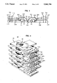
- FIG. 8 illustrates a rectangular cluster of stacked assemblies.
- FIG. 1 shows a preferred embodiment of an integrated circuit package 10 in accordance with the invention comprising a thermally conductive plate 11 and an open rectangular structure 20, comprising layers of conductor and insulator and presenting one or more linear arrays of electrically conductive bonding pads.
- side 20A provides a lower linear array of bonding pads (B 11 , B 12 , . . . , B 1n ) and an upper linear array (B 21 , B 22 , . . . , B 2n ).
- Opposing side 20B provides lower array (B 31 , B 32 , . . . , B 3n ) (not shown) and upper array (B 41 , B 42 , . . .
- each bonding pad B ij is provided with lateral conductive connecting portion extending laterally from the bonding pad on the inside edge of the rectangular structure 20, through the structure to a respective lateral contact L ij on the transverse outside edge of 20.
- each bonding pad B ij is also conductively connected through the rectangular structure 20 to a respective transverse contact T ij on a lateral edge of 20.
- the transverse contacts can extend completely through structure 20 to provide contact points T ij on both the upper lateral surface of 20 and the lower lateral surface (not shown in FIG. 1).
- plate 11 includes fin regions 12 extending beyond the external edges of rectangular structure 20 for acting as cooling fins.
- the linear arrays B ij and the cooling fins 12 are on different pairs of opposing parallel sides of 20.
- Advantageously rectangular structure 20 is provided with alignment means such as a plurality of openings 25, one in each corner, for use in aligning a plurality of such structures in an assembly.
- alignment means such as a plurality of openings 25, one in each corner, for use in aligning a plurality of such structures in an assembly.
- the central opening in rectangular structure 20 is chosen so that the structure 20 can receive and laterally surround an integrated circuit 200 mounted on plate 11.
- the circuit 200 comprises a set of contacts C 1 , C 2 , . . . , C n to which interconnection is desired, and these contacts C i are electrically connected to the set of bonding pads B ij preferably by gold wire bonds 210 in accordance with techniques well known in the art.
- FIG. 3 is a schematic cross section of the structure of FIG. 2 useful in showing the interconnections provided by the invention.
- contact C 1 on integrated circuit can be connected by wire 210 to bonding pad B 14 which, in turn, is connected to lateral contact point L 14 and transverse contact T 14 .
- C 2 is connected to bonding pad B 24 and thence to L 24 and T 24 .
- FIG. 4 is an exploded view showing the principal components used in making a preferred rectangular structure 20.
- the structure 20 is built of a plurality of layers L 1 through L 6 of unsintered ceramic tape having an array of registered drilled apertures (D 11 , D 12 , D 13 , D 14 , D 21 . . . , D m4 ) in which transverse conductive connectors T ij can be formed. And upon the layers are printed conductive segments forming the lateral conductive connectors L ij .
- the interior transverse surface of the rectangular structure presents two linear arrays of bonding pads B ij and one pair of bonding pads from each array is mapped into a single column of conductively filled apertures D ij .
- pads B 15 and B 16 of the lower array and pads B 25 and B 26 of the upper array are connected by conductively filled apertures to transverse contacts T 16 , T 15 , T 25 and T 26 .
- the lateral connections can effect crossovers by going up a level or down a level as is done in connecting B 16 to L 16 and B 26 to L 26 .
- the ceramic layers L 1 -L 6 are comprised of 0.04 inch thick green ceramic tape--a mixture of aluminum oxide ceramic powder and organic binder--such as Coors ceramic tape available from Coors Ceramic Corporation, Boulder, Colo.
- the apertures D ij can be 141/2 mils in diameter, and both the transverse and lateral connectors can be metallized with a screen printable ink containing tungsten metal particles such as Tungsten Ink marketed by Cernonics, Inc., Matawan, N.J.
- the conductive plate 11 can be a tungsten-copper alloy, such as Elkinite, having a coefficient of thermal expansion compatible with the ceramic.
- the layers L 1 -L 6 are assembled in proper order and registration, pressed together at a pressure of 500 pounds per square inch and heated to a temperature of 70° C. for about 1 min to soften the binder and cause the individual layers to bond together.
- Final consolidation of the structure is effected by co-sintering the ceramic and the tungsten, as by sintering at 1625° ⁇ 25° C. for 2 to 8 hours in a wet (dew point 70° C.) 80% N 2 by volume, 20% H 2 furnace atmosphere.
- the exposed metallized areas of the structure can then be electroplated with a pure nickel film about 0.0005 inch thick.
- Conductive plate 11 is then brazed to the lower lateral surface, and the metallized areas of the structure and the conductive plate can be electroplated with a gold film about 0.0002 inch thick.
- the result is an integral structure 20 with internal transverse and lateral connectors.
- an integrated circuit package in accordance with the invention comprises (1) a thermally conductive plate for supporting an integrated circuit and (2) an open rectangular structure having a central opening, exterior and interior transverse surfaces with respect to the central opening and parallel lateral surfaces.
- the rectangular structure is mounted on the conductive plate with the interior transverse surfaces positioned for extending around the periphery of the integrated circuit.
- At least one of the interior transverse surfaces of the rectangular structure presents at least one linear array of contact means (bonding pads) for interconnection with contacts on the integrated circuit.
- Each of the contact means is provided with an electrical connection laterally through the rectangular structure to the exterior transverse surface, and each of the contact means is provided with an electrical connection transversely through the rectangular structure to the overlying lateral surface.
- each one of a pair of opposing interior transverse surfaces of the open rectangular structure presents two linear arrays of contact means (bonding pads) for interconnection with contacts on the integrated circuit.
- the thermally conductive plate has portions extending beyond the exterior transverse surfaces of the other (remaining) pair of opposing surfaces for acting as cooling fins.
- the rectangular structure is provided with alignment means for aligning a bottom lateral surface of the package upon a top lateral surface of another such package.
- This alignment means can be a set of drilled openings in each of the four corner regions extending transversely through the rectangular structure.
- FIG. 5 is a schematic illustration of a stacked assembly 400 of integrated circuit packages in accordance with the invention.
- a plurality of m similarly oriented packages 10 are stacked one on top of the other to form a rectangular parallelpiped having a plurality of parallel planar cooling fins 12 projecting from a first pair of aligned transverse surfaces 410A and 410B and a second pair of aligned transverse surfaces 420A and 420B providing planar rectangular arrays 430 of lateral contact points to the enclosed integrated circuits.
- the surface area of each contact point (L ij of FIGS. 1-4) can be enhanced by depositing an array of gold pads onto the contact points.
- This planar array 430 defines a contact plane which can be used in interconnecting assemblies.
- Interconnection between the transverse contacts T ij of the respective stacked packages can be facilitated by disposing between the packages thin sheets of anisotropic conductive material (not shown) such as the 25 mil EPCI material marketed by AT&T Microelectronics, Allentown, Pa. This material, comprising conductive particles in a silicone binding, selectively conducts in regions of compression between overlying contact points.
- anisotropic conductive material such as the 25 mil EPCI material marketed by AT&T Microelectronics, Allentown, Pa.
- This material comprising conductive particles in a silicone binding, selectively conducts in regions of compression between overlying contact points.
- a thin insulating layer such as mylar can be interposed.
- the stacked assembly is bolted together by threaded vertical rods 440, through respective corresponding apertures 25 in each corner of each package 10.
- an assembly of integrated circuit packages in accordance with the invention comprises a plurality of integrated circuit packages, as described above, stacked one above the other with their respective exterior transverse surfaces aligned in a contact plane.
- the respective cooling fin portions are oriented in the same direction, the transverse openings in the corner regions are in alignment, and the plurality of packages is secured together in alignment by a rigid bolt through the aligned openings.
- larger scale interconnections can comprise a linear cluster 500 of plural assemblies 400A, 400B and 400C.
- the stacked assemblies are preferably oriented with their respective contact surfaces (not shown) parallel and adjacent.
- the arrangement is designed so that desired interconnections between one assembly, e.g., 400A, and the adjacent assembly, e.g. 400B, are effected by contact between a contact plane 430 of 400A (not shown) and a contact plane 430 of 400B.
- Such contact can be facilitated by interposing a sheet 550 of EPCI material between the planar arrays.
- the contacts of 400A, i.e. the set P ij would contact respective contacts P' ij of 400B.
- a transformation plane 560 can be disposed between 400A and 400B, to provide by suitable insulated interconnections, any desired mapping of contacts P ij into contacts P' ij .
- FIG. 7 shows a particularly advantageous embodiment of the invention comprising a linear cluster 500 of plural assemblies 400A, 400B, and 400C similar to the cluster shown in FIG. 6 except that the middle assembly 400B is rotated 90° about the axis of the array.
- the contact planar arrays 430 of assembly 400B preferably each provide a square m ⁇ m matrix of contact points P ij where m is the number of packages in assembly 400B.
- assemblies 400A and 400C each comprise m packages and preferably each provide a contact planar array comprising a m ⁇ m matrix of contact points.
- each package in assembly 400B is provided contact with each of the m packages in assembly 400C on the right and with each of the m packages in assembly 400A on the left.
- each integrated circuit in assembly 400B can be provided contact with each integrated circuit in the entire cluster.
- this linear cluster could be lengthened, as by adding an additional assembly 400D (not shown) rotated by 90° so that 400D is oriented similar to 400B. 400D would provide each of its packages contact with each of the m packages in neighboring assembly 400C.
- a linear cluster of assemblies of integrated circuit packages in accordance with the invention comprises a plurality of integrated circuit assemblies, as described above, disposed in a linear array with a contact plane of each respective assembly opposing and contacting a contact plane of at least one other assembly.
- the cluster comprises at least three integrated circuit assemblies each having square contact matrices, and the middle assembly of the linear array is rotated by 90° about the axis of the array so that each integrated circuit package of the middle assembly has at least one contact with every integrated circuit package of each neighboring assembly.
- each package 400A-400I has been modified by the elimination of fins on one or both sides and interconnections through the packages are provided on the sides where the fins have been removed. Stacked assemblies are then disposed in a rectangular array with each assembly electrically interconnected to one or more of its neighbors as described above. It is thus seen that the integrated circuit package of the invention provides a wide variety of highly compact assemblies and clusters rich in interconnections among the enclosed circuits.
Landscapes
- Engineering & Computer Science (AREA)
- Microelectronics & Electronic Packaging (AREA)
- Power Engineering (AREA)
- Physics & Mathematics (AREA)
- Condensed Matter Physics & Semiconductors (AREA)
- General Physics & Mathematics (AREA)
- Computer Hardware Design (AREA)
- Chemical & Material Sciences (AREA)
- Materials Engineering (AREA)
- Cooling Or The Like Of Semiconductors Or Solid State Devices (AREA)
- Cooling Or The Like Of Electrical Apparatus (AREA)
Abstract
Description
Claims (7)
Priority Applications (4)
| Application Number | Priority Date | Filing Date | Title |
|---|---|---|---|
| US07/587,308 US5043794A (en) | 1990-09-24 | 1990-09-24 | Integrated circuit package and compact assemblies thereof |
| CA002046253A CA2046253C (en) | 1990-09-24 | 1991-07-04 | Integrated circuit package and compact assemblies thereof |
| EP19910308391 EP0478188A3 (en) | 1990-09-24 | 1991-09-13 | Integrated circuit package and compact assemblies thereof |
| JP3265518A JPH0821644B2 (en) | 1990-09-24 | 1991-09-18 | Integrated circuit package and its assembly and cluster |
Applications Claiming Priority (1)
| Application Number | Priority Date | Filing Date | Title |
|---|---|---|---|
| US07/587,308 US5043794A (en) | 1990-09-24 | 1990-09-24 | Integrated circuit package and compact assemblies thereof |
Publications (1)
| Publication Number | Publication Date |
|---|---|
| US5043794A true US5043794A (en) | 1991-08-27 |
Family
ID=24349283
Family Applications (1)
| Application Number | Title | Priority Date | Filing Date |
|---|---|---|---|
| US07/587,308 Expired - Lifetime US5043794A (en) | 1990-09-24 | 1990-09-24 | Integrated circuit package and compact assemblies thereof |
Country Status (4)
| Country | Link |
|---|---|
| US (1) | US5043794A (en) |
| EP (1) | EP0478188A3 (en) |
| JP (1) | JPH0821644B2 (en) |
| CA (1) | CA2046253C (en) |
Cited By (46)
| Publication number | Priority date | Publication date | Assignee | Title |
|---|---|---|---|---|
| US5142352A (en) * | 1989-07-11 | 1992-08-25 | Oxley Developments Company Limited | Ceramic package component having one quarter wavelength spaced conductive grounding vias |
| US5157480A (en) * | 1991-02-06 | 1992-10-20 | Motorola, Inc. | Semiconductor device having dual electrical contact sites |
| US5225709A (en) * | 1990-06-15 | 1993-07-06 | Hitachi, Ltd. | Package having a structure for stabilizing and/or impedance-matching a semiconductor IC device accommodated therein |
| WO1993018549A1 (en) * | 1992-03-13 | 1993-09-16 | Thomson-Csf | Process and device for three-dimensional interconnection of housings for electronic components |
| US5343075A (en) * | 1991-06-29 | 1994-08-30 | Sony Corporation | Composite stacked semiconductor device with contact plates |
| WO1995000972A1 (en) * | 1993-06-28 | 1995-01-05 | Harris Corporation | Multilayer ltcc tub architecture for hermetically sealing semiconductor die, external electrical access for which is provided by way of sidewall recesses |
| EP0658937A1 (en) * | 1993-12-08 | 1995-06-21 | Hughes Aircraft Company | Vertical IC chip stack with discrete chip carriers formed from dielectric tape |
| US5434745A (en) * | 1994-07-26 | 1995-07-18 | White Microelectronics Div. Of Bowmar Instrument Corp. | Stacked silicon die carrier assembly |
| EP0669653A1 (en) * | 1994-02-21 | 1995-08-30 | ABB Management AG | Power semiconductor module and circuit arrangement with at least two semiconductor modules |
| US5497031A (en) * | 1993-09-24 | 1996-03-05 | Kabushiki Kaisha Toshiba | Semiconductor device having semiconductor chip with backside electrode |
| US5500555A (en) * | 1994-04-11 | 1996-03-19 | Lsi Logic Corporation | Multi-layer semiconductor package substrate with thermally-conductive prepeg layer |
| US5514907A (en) * | 1995-03-21 | 1996-05-07 | Simple Technology Incorporated | Apparatus for stacking semiconductor chips |
| US5633530A (en) * | 1995-10-24 | 1997-05-27 | United Microelectronics Corporation | Multichip module having a multi-level configuration |
| US5633783A (en) * | 1994-09-29 | 1997-05-27 | Fujitsu Limited | Multi-chip ceramic module for mounting electric parts on both substrate and cap connected through interconnecting pins |
| EP0807369A1 (en) * | 1995-01-23 | 1997-11-19 | Irvine Sensors Corporation | Stackable modules and multimodular assemblies |
| US5838060A (en) * | 1995-12-12 | 1998-11-17 | Comer; Alan E. | Stacked assemblies of semiconductor packages containing programmable interconnect |
| US5847448A (en) * | 1990-12-11 | 1998-12-08 | Thomson-Csf | Method and device for interconnecting integrated circuits in three dimensions |
| US5977623A (en) * | 1996-10-04 | 1999-11-02 | Lg Semicon Co., Ltd. | Semiconductor package and socket thereof and methods of fabricating same |
| US6023098A (en) * | 1995-06-29 | 2000-02-08 | Fujitsu Limited | Semiconductor device having terminals for heat radiation |
| US6031284A (en) * | 1997-03-14 | 2000-02-29 | Lg Semicon Co., Ltd. | Package body and semiconductor chip package using same |
| US6137163A (en) * | 1997-09-12 | 2000-10-24 | Hyundai Electronics Industries Co., Ltd. | Semiconductor substrate and stackable semiconductor package and fabrication method thereof |
| US6172423B1 (en) * | 1997-11-15 | 2001-01-09 | Hyundai Electronics Industries Co., Ltd. | Layer-type ball grid array semiconductor package and fabrication method thereof |
| US6235554B1 (en) * | 1995-11-27 | 2001-05-22 | Micron Technology, Inc. | Method for fabricating stackable chip scale semiconductor package |
| US6376769B1 (en) | 1999-05-18 | 2002-04-23 | Amerasia International Technology, Inc. | High-density electronic package, and method for making same |
| US6462408B1 (en) | 2001-03-27 | 2002-10-08 | Staktek Group, L.P. | Contact member stacking system and method |
| US6580031B2 (en) | 2000-03-14 | 2003-06-17 | Amerasia International Technology, Inc. | Method for making a flexible circuit interposer having high-aspect ratio conductors |
| US6608763B1 (en) | 2000-09-15 | 2003-08-19 | Staktek Group L.P. | Stacking system and method |
| US20040159462A1 (en) * | 1999-06-01 | 2004-08-19 | Chung Kevin Kwong-Tai | Flexible dielectric electronic substrate and method for making same |
| US20050221633A1 (en) * | 2004-03-30 | 2005-10-06 | Wildes Douglas G | High-density connection between multiple circuit boards |
| US7066741B2 (en) | 1999-09-24 | 2006-06-27 | Staktek Group L.P. | Flexible circuit connector for stacked chip module |
| US20060162957A1 (en) * | 2005-01-24 | 2006-07-27 | Jorg Kindermann | Printed circuit board, printed circuit module and method for producing a printed circuit board |
| DE19963264B4 (en) * | 1999-12-17 | 2007-05-31 | Optotransmitter-Umweltschutz-Technologie E.V. | Carrier material for high-performance electronic components in SMD design and a high-performance electronic component produced therewith |
| US20080023853A1 (en) * | 1995-12-19 | 2008-01-31 | Micron Technology, Inc. | Flip chip adaptor package for bare die |
| US20080224298A1 (en) * | 2007-03-12 | 2008-09-18 | Micron Technology, Inc. | Apparatus for packaging semiconductor devices, packaged semiconductor components, methods of manufacturing apparatus for packaging semiconductor devices, and methods of manufacturing semiconductor components |
| US20080291637A1 (en) * | 2007-05-21 | 2008-11-27 | Universal Scientific Industrial Co., Ltd. | Small-sized communication module package |
| US20090097214A1 (en) * | 2007-10-15 | 2009-04-16 | Samsung Techwin Co., Ltd | Electronic chip embedded circuit board and method of manufacturing the same |
| US7714426B1 (en) * | 2007-07-07 | 2010-05-11 | Keith Gann | Ball grid array package format layers and structure |
| US20110037164A1 (en) * | 2005-12-29 | 2011-02-17 | Wavenics, Inc. | Three-dimensional package module, method of fabricating the same, and method of fabricating passive device applied to the three-dimensional package module |
| USRE43112E1 (en) | 1998-05-04 | 2012-01-17 | Round Rock Research, Llc | Stackable ball grid array package |
| USRE43536E1 (en) | 2002-02-07 | 2012-07-24 | Aprolase Development Co., Llc | Stackable layer containing ball grid array package |
| CN103311214A (en) * | 2013-05-14 | 2013-09-18 | 中国科学院微电子研究所 | Substrate for laminated packaging |
| US20140097533A1 (en) * | 2011-12-21 | 2014-04-10 | Huawei Technologies Co., Ltd. | Pop Package Structure |
| US20160299361A1 (en) * | 2015-04-07 | 2016-10-13 | Lumentum Operations Llc | High bandwidth rf or microwave interconnects for optical modulators |
| CN106098632B (en) * | 2016-06-20 | 2018-12-25 | 浦江正裕文化传播有限公司 | A kind of structure improved integrated antenna package |
| US20190157197A1 (en) * | 2017-11-22 | 2019-05-23 | Advanced Semiconductor Engineering, Inc. | Semiconductor device package |
| US10420218B2 (en) * | 2015-09-15 | 2019-09-17 | Safran Electronics & Defense | Compact electronic system and device comprising such a system |
Families Citing this family (7)
| Publication number | Priority date | Publication date | Assignee | Title |
|---|---|---|---|---|
| FR2696871B1 (en) * | 1992-10-13 | 1994-11-18 | Thomson Csf | Method of 3D interconnection of housings of electronic components, and 3D components resulting therefrom. |
| US6320257B1 (en) * | 1994-09-27 | 2001-11-20 | Foster-Miller, Inc. | Chip packaging technique |
| JP2944449B2 (en) * | 1995-02-24 | 1999-09-06 | 日本電気株式会社 | Semiconductor package and manufacturing method thereof |
| US5572405A (en) * | 1995-06-07 | 1996-11-05 | International Business Machines Corporation (Ibm) | Thermally enhanced ball grid array package |
| US6627980B2 (en) | 2001-04-12 | 2003-09-30 | Formfactor, Inc. | Stacked semiconductor device assembly with microelectronic spring contacts |
| FR2845821B1 (en) * | 2002-10-11 | 2005-12-02 | Thales Sa | ELECTRONIC SUBSTRATE OF A THREE-DIMENSIONAL ELECTRONIC MODULE HAVING A HIGH THERMAL DISSIPATION POWER AND ELECTRONIC MODULE |
| CN106098635B (en) * | 2016-08-22 | 2018-07-27 | 东莞立德电子有限公司 | A kind of integrated antenna package of structure optimization |
Citations (8)
| Publication number | Priority date | Publication date | Assignee | Title |
|---|---|---|---|---|
| US4631572A (en) * | 1983-09-27 | 1986-12-23 | Trw Inc. | Multiple path signal distribution to large scale integration chips |
| US4638348A (en) * | 1982-08-10 | 1987-01-20 | Brown David F | Semiconductor chip carrier |
| US4654694A (en) * | 1983-07-29 | 1987-03-31 | Compagnie D'informatique Militaire Spatiale Et Aeronautique | Electronic component box supplied with a capacitor |
| US4879588A (en) * | 1987-01-19 | 1989-11-07 | Sumitomo Electric Industries, Ltd. | Integrated circuit package |
| US4890153A (en) * | 1986-04-04 | 1989-12-26 | Fairchild Semiconductor Corporation | Single bonding shelf, multi-row wire-bond finger layout for integrated circuit package |
| US4894706A (en) * | 1985-02-14 | 1990-01-16 | Nippon Telegraph And Telephone Corporation | Three-dimensional packaging of semiconductor device chips |
| US4953005A (en) * | 1987-04-17 | 1990-08-28 | Xoc Devices, Inc. | Packaging system for stacking integrated circuits |
| US4956694A (en) * | 1988-11-04 | 1990-09-11 | Dense-Pac Microsystems, Inc. | Integrated circuit chip stacking |
Family Cites Families (7)
| Publication number | Priority date | Publication date | Assignee | Title |
|---|---|---|---|---|
| US4551746A (en) | 1982-10-05 | 1985-11-05 | Mayo Foundation | Leadless chip carrier apparatus providing an improved transmission line environment and improved heat dissipation |
| JPH0797616B2 (en) * | 1986-08-19 | 1995-10-18 | 新光電気工業株式会社 | Method for manufacturing semiconductor device |
| JPS6362364A (en) * | 1986-09-03 | 1988-03-18 | Nec Corp | Package of semiconductor integrated circuit |
| US4868712A (en) | 1987-02-04 | 1989-09-19 | Woodman John K | Three dimensional integrated circuit package |
| JPS63258046A (en) * | 1987-04-15 | 1988-10-25 | Toshiba Corp | Semiconductor integrated circuit device |
| US4858072A (en) | 1987-11-06 | 1989-08-15 | Ford Aerospace & Communications Corporation | Interconnection system for integrated circuit chips |
| JP2810130B2 (en) * | 1989-07-26 | 1998-10-15 | 松下電工株式会社 | Semiconductor package |
-
1990
- 1990-09-24 US US07/587,308 patent/US5043794A/en not_active Expired - Lifetime
-
1991
- 1991-07-04 CA CA002046253A patent/CA2046253C/en not_active Expired - Fee Related
- 1991-09-13 EP EP19910308391 patent/EP0478188A3/en not_active Ceased
- 1991-09-18 JP JP3265518A patent/JPH0821644B2/en not_active Expired - Lifetime
Patent Citations (8)
| Publication number | Priority date | Publication date | Assignee | Title |
|---|---|---|---|---|
| US4638348A (en) * | 1982-08-10 | 1987-01-20 | Brown David F | Semiconductor chip carrier |
| US4654694A (en) * | 1983-07-29 | 1987-03-31 | Compagnie D'informatique Militaire Spatiale Et Aeronautique | Electronic component box supplied with a capacitor |
| US4631572A (en) * | 1983-09-27 | 1986-12-23 | Trw Inc. | Multiple path signal distribution to large scale integration chips |
| US4894706A (en) * | 1985-02-14 | 1990-01-16 | Nippon Telegraph And Telephone Corporation | Three-dimensional packaging of semiconductor device chips |
| US4890153A (en) * | 1986-04-04 | 1989-12-26 | Fairchild Semiconductor Corporation | Single bonding shelf, multi-row wire-bond finger layout for integrated circuit package |
| US4879588A (en) * | 1987-01-19 | 1989-11-07 | Sumitomo Electric Industries, Ltd. | Integrated circuit package |
| US4953005A (en) * | 1987-04-17 | 1990-08-28 | Xoc Devices, Inc. | Packaging system for stacking integrated circuits |
| US4956694A (en) * | 1988-11-04 | 1990-09-11 | Dense-Pac Microsystems, Inc. | Integrated circuit chip stacking |
Cited By (79)
| Publication number | Priority date | Publication date | Assignee | Title |
|---|---|---|---|---|
| US5142352A (en) * | 1989-07-11 | 1992-08-25 | Oxley Developments Company Limited | Ceramic package component having one quarter wavelength spaced conductive grounding vias |
| US5225709A (en) * | 1990-06-15 | 1993-07-06 | Hitachi, Ltd. | Package having a structure for stabilizing and/or impedance-matching a semiconductor IC device accommodated therein |
| US5847448A (en) * | 1990-12-11 | 1998-12-08 | Thomson-Csf | Method and device for interconnecting integrated circuits in three dimensions |
| US5157480A (en) * | 1991-02-06 | 1992-10-20 | Motorola, Inc. | Semiconductor device having dual electrical contact sites |
| US5343075A (en) * | 1991-06-29 | 1994-08-30 | Sony Corporation | Composite stacked semiconductor device with contact plates |
| WO1993018549A1 (en) * | 1992-03-13 | 1993-09-16 | Thomson-Csf | Process and device for three-dimensional interconnection of housings for electronic components |
| FR2688630A1 (en) * | 1992-03-13 | 1993-09-17 | Thomson Csf | METHOD AND DEVICE FOR THREE-DIMENSIONAL INTERCONNECTION OF ELECTRONIC COMPONENT PACKAGES. |
| US5885850A (en) * | 1992-03-13 | 1999-03-23 | Thomson-Csf | Method for the 3D interconnection of packages of electronic components, and device obtained by this method |
| WO1995000972A1 (en) * | 1993-06-28 | 1995-01-05 | Harris Corporation | Multilayer ltcc tub architecture for hermetically sealing semiconductor die, external electrical access for which is provided by way of sidewall recesses |
| US5455385A (en) * | 1993-06-28 | 1995-10-03 | Harris Corporation | Multilayer LTCC tub architecture for hermetically sealing semiconductor die, external electrical access for which is provided by way of sidewall recesses |
| US5497031A (en) * | 1993-09-24 | 1996-03-05 | Kabushiki Kaisha Toshiba | Semiconductor device having semiconductor chip with backside electrode |
| EP0658937A1 (en) * | 1993-12-08 | 1995-06-21 | Hughes Aircraft Company | Vertical IC chip stack with discrete chip carriers formed from dielectric tape |
| US5600541A (en) * | 1993-12-08 | 1997-02-04 | Hughes Aircraft Company | Vertical IC chip stack with discrete chip carriers formed from dielectric tape |
| EP0669653A1 (en) * | 1994-02-21 | 1995-08-30 | ABB Management AG | Power semiconductor module and circuit arrangement with at least two semiconductor modules |
| US5500555A (en) * | 1994-04-11 | 1996-03-19 | Lsi Logic Corporation | Multi-layer semiconductor package substrate with thermally-conductive prepeg layer |
| US5434745A (en) * | 1994-07-26 | 1995-07-18 | White Microelectronics Div. Of Bowmar Instrument Corp. | Stacked silicon die carrier assembly |
| US5633783A (en) * | 1994-09-29 | 1997-05-27 | Fujitsu Limited | Multi-chip ceramic module for mounting electric parts on both substrate and cap connected through interconnecting pins |
| EP0807369A1 (en) * | 1995-01-23 | 1997-11-19 | Irvine Sensors Corporation | Stackable modules and multimodular assemblies |
| US5701233A (en) * | 1995-01-23 | 1997-12-23 | Irvine Sensors Corporation | Stackable modules and multimodular assemblies |
| EP0807369A4 (en) * | 1995-01-23 | 1999-11-17 | Irvine Sensors Corp | Stackable modules and multimodular assemblies |
| US5514907A (en) * | 1995-03-21 | 1996-05-07 | Simple Technology Incorporated | Apparatus for stacking semiconductor chips |
| USRE36916E (en) * | 1995-03-21 | 2000-10-17 | Simple Technology Incorporated | Apparatus for stacking semiconductor chips |
| US6023098A (en) * | 1995-06-29 | 2000-02-08 | Fujitsu Limited | Semiconductor device having terminals for heat radiation |
| US5633530A (en) * | 1995-10-24 | 1997-05-27 | United Microelectronics Corporation | Multichip module having a multi-level configuration |
| US6235554B1 (en) * | 1995-11-27 | 2001-05-22 | Micron Technology, Inc. | Method for fabricating stackable chip scale semiconductor package |
| US5838060A (en) * | 1995-12-12 | 1998-11-17 | Comer; Alan E. | Stacked assemblies of semiconductor packages containing programmable interconnect |
| US8164175B2 (en) | 1995-12-19 | 2012-04-24 | Round Rock Research, Llc | Stackable semiconductor device assemblies |
| US8049317B2 (en) | 1995-12-19 | 2011-11-01 | Round Rock Research, Llc | Grid array packages |
| US7329945B2 (en) | 1995-12-19 | 2008-02-12 | Micron Technology, Inc. | Flip-chip adaptor package for bare die |
| US20080023853A1 (en) * | 1995-12-19 | 2008-01-31 | Micron Technology, Inc. | Flip chip adaptor package for bare die |
| US20100148352A1 (en) * | 1995-12-19 | 2010-06-17 | Micron Technology, Inc. | Grid array packages and assemblies including the same |
| US8299598B2 (en) | 1995-12-19 | 2012-10-30 | Round Rock Research, Llc | Grid array packages and assemblies including the same |
| US8198138B2 (en) | 1995-12-19 | 2012-06-12 | Round Rock Research, Llc | Methods for providing and using grid array packages |
| US7381591B2 (en) | 1995-12-19 | 2008-06-03 | Micron Technology, Inc. | Flip-chip adaptor package for bare die |
| US20100155966A1 (en) * | 1995-12-19 | 2010-06-24 | Micron Technology, Inc. | Grid array packages |
| US20100155930A1 (en) * | 1995-12-19 | 2010-06-24 | Micron Technology, Inc. | Stackable semiconductor device assemblies |
| US5977623A (en) * | 1996-10-04 | 1999-11-02 | Lg Semicon Co., Ltd. | Semiconductor package and socket thereof and methods of fabricating same |
| US6031284A (en) * | 1997-03-14 | 2000-02-29 | Lg Semicon Co., Ltd. | Package body and semiconductor chip package using same |
| DE19802347B4 (en) * | 1997-09-12 | 2005-10-06 | LG Semicon Co., Ltd., Cheongju | A stackable semiconductor substrate and stackable semiconductor device, and manufacturing methods thereof, and a semiconductor stackable module module manufacturing method |
| US6137163A (en) * | 1997-09-12 | 2000-10-24 | Hyundai Electronics Industries Co., Ltd. | Semiconductor substrate and stackable semiconductor package and fabrication method thereof |
| US6172423B1 (en) * | 1997-11-15 | 2001-01-09 | Hyundai Electronics Industries Co., Ltd. | Layer-type ball grid array semiconductor package and fabrication method thereof |
| USRE43112E1 (en) | 1998-05-04 | 2012-01-17 | Round Rock Research, Llc | Stackable ball grid array package |
| US6376769B1 (en) | 1999-05-18 | 2002-04-23 | Amerasia International Technology, Inc. | High-density electronic package, and method for making same |
| US20040159462A1 (en) * | 1999-06-01 | 2004-08-19 | Chung Kevin Kwong-Tai | Flexible dielectric electronic substrate and method for making same |
| US7154046B2 (en) | 1999-06-01 | 2006-12-26 | Amerasia International Technology, Inc. | Flexible dielectric electronic substrate and method for making same |
| US7066741B2 (en) | 1999-09-24 | 2006-06-27 | Staktek Group L.P. | Flexible circuit connector for stacked chip module |
| DE19963264B4 (en) * | 1999-12-17 | 2007-05-31 | Optotransmitter-Umweltschutz-Technologie E.V. | Carrier material for high-performance electronic components in SMD design and a high-performance electronic component produced therewith |
| US6580031B2 (en) | 2000-03-14 | 2003-06-17 | Amerasia International Technology, Inc. | Method for making a flexible circuit interposer having high-aspect ratio conductors |
| US6608763B1 (en) | 2000-09-15 | 2003-08-19 | Staktek Group L.P. | Stacking system and method |
| US6462408B1 (en) | 2001-03-27 | 2002-10-08 | Staktek Group, L.P. | Contact member stacking system and method |
| US6806120B2 (en) | 2001-03-27 | 2004-10-19 | Staktek Group, L.P. | Contact member stacking system and method |
| USRE43536E1 (en) | 2002-02-07 | 2012-07-24 | Aprolase Development Co., Llc | Stackable layer containing ball grid array package |
| US6974333B2 (en) * | 2004-03-30 | 2005-12-13 | General Electric Company | High-density connection between multiple circuit boards |
| US20050221633A1 (en) * | 2004-03-30 | 2005-10-06 | Wildes Douglas G | High-density connection between multiple circuit boards |
| US20060162957A1 (en) * | 2005-01-24 | 2006-07-27 | Jorg Kindermann | Printed circuit board, printed circuit module and method for producing a printed circuit board |
| US20110037164A1 (en) * | 2005-12-29 | 2011-02-17 | Wavenics, Inc. | Three-dimensional package module, method of fabricating the same, and method of fabricating passive device applied to the three-dimensional package module |
| US8034664B2 (en) * | 2005-12-29 | 2011-10-11 | Wavenics Inc. | Method of fabricating passive device applied to the three-dimensional package module |
| WO2008112643A3 (en) * | 2007-03-12 | 2008-12-18 | Micron Technology Inc | Apparatus for packaging semiconductor devices, packaged semiconductor components, methods of manufacturing apparatus for packaging semiconductor devices, and methods of manufacturing semiconductor components |
| US20080224298A1 (en) * | 2007-03-12 | 2008-09-18 | Micron Technology, Inc. | Apparatus for packaging semiconductor devices, packaged semiconductor components, methods of manufacturing apparatus for packaging semiconductor devices, and methods of manufacturing semiconductor components |
| US7759785B2 (en) | 2007-03-12 | 2010-07-20 | Micron Technology, Inc. | Apparatus for packaging semiconductor devices, packaged semiconductor components, methods of manufacturing apparatus for packaging semiconductor devices, and methods of manufacturing semiconductor components |
| KR101407773B1 (en) | 2007-03-12 | 2014-07-02 | 마이크론 테크놀로지, 인크 | Apparatus for packaging semiconductor devices, packaged semiconductor components, methods of manufacturing apparatus for packaging semiconductor devices, and methods of manufacturing semiconductor components |
| US20100279466A1 (en) * | 2007-03-12 | 2010-11-04 | Micron Technology, Inc. | Apparatus for packaging semiconductor devices, packaged semiconductor components, methods of manufacturing apparatus for packaging semiconductor devices, and methods of manufacturing semiconductor components |
| WO2008112643A2 (en) | 2007-03-12 | 2008-09-18 | Micron Technology, Inc. | Apparatus for packaging semiconductor devices, packaged semiconductor components, methods of manufacturing apparatus for packaging semiconductor devices, and methods of manufacturing semiconductor components |
| US8138021B2 (en) | 2007-03-12 | 2012-03-20 | Micron Technology, Inc. | Apparatus for packaging semiconductor devices, packaged semiconductor components, methods of manufacturing apparatus for packaging semiconductor devices, and methods of manufacturing semiconductor components |
| US20080291637A1 (en) * | 2007-05-21 | 2008-11-27 | Universal Scientific Industrial Co., Ltd. | Small-sized communication module package |
| US7982300B2 (en) | 2007-07-07 | 2011-07-19 | Aprolase Development Co., Llc | Stackable layer containing ball grid array package |
| US20100181662A1 (en) * | 2007-07-07 | 2010-07-22 | Keith Gann | Stackable layer containing ball grid array package |
| US7714426B1 (en) * | 2007-07-07 | 2010-05-11 | Keith Gann | Ball grid array package format layers and structure |
| US8835218B2 (en) | 2007-07-07 | 2014-09-16 | Aprolase Development Co., Llc | Stackable layer containing ball grid array package |
| US20090097214A1 (en) * | 2007-10-15 | 2009-04-16 | Samsung Techwin Co., Ltd | Electronic chip embedded circuit board and method of manufacturing the same |
| US9318407B2 (en) * | 2011-12-21 | 2016-04-19 | Huawei Technologies Co., Ltd. | Pop package structure |
| US20140097533A1 (en) * | 2011-12-21 | 2014-04-10 | Huawei Technologies Co., Ltd. | Pop Package Structure |
| CN103311214A (en) * | 2013-05-14 | 2013-09-18 | 中国科学院微电子研究所 | Substrate for laminated packaging |
| US20160299361A1 (en) * | 2015-04-07 | 2016-10-13 | Lumentum Operations Llc | High bandwidth rf or microwave interconnects for optical modulators |
| US10502987B2 (en) * | 2015-04-07 | 2019-12-10 | Lumentum Operations Llc | High bandwidth RF or microwave interconnects for optical modulators |
| US10420218B2 (en) * | 2015-09-15 | 2019-09-17 | Safran Electronics & Defense | Compact electronic system and device comprising such a system |
| CN106098632B (en) * | 2016-06-20 | 2018-12-25 | 浦江正裕文化传播有限公司 | A kind of structure improved integrated antenna package |
| US20190157197A1 (en) * | 2017-11-22 | 2019-05-23 | Advanced Semiconductor Engineering, Inc. | Semiconductor device package |
| US10672696B2 (en) * | 2017-11-22 | 2020-06-02 | Advanced Semiconductor Engineering, Inc. | Semiconductor device package |
Also Published As
| Publication number | Publication date |
|---|---|
| CA2046253C (en) | 1995-09-05 |
| CA2046253A1 (en) | 1992-03-25 |
| EP0478188A2 (en) | 1992-04-01 |
| JPH04234199A (en) | 1992-08-21 |
| EP0478188A3 (en) | 1992-07-08 |
| JPH0821644B2 (en) | 1996-03-04 |
Similar Documents
| Publication | Publication Date | Title |
|---|---|---|
| US5043794A (en) | Integrated circuit package and compact assemblies thereof | |
| US4763188A (en) | Packaging system for multiple semiconductor devices | |
| US5600541A (en) | Vertical IC chip stack with discrete chip carriers formed from dielectric tape | |
| US5943213A (en) | Three-dimensional electronic module | |
| JP2960276B2 (en) | Multilayer wiring board, semiconductor device using this substrate, and method of manufacturing multilayer wiring board | |
| US5016138A (en) | Three dimensional integrated circuit package | |
| US5241456A (en) | Compact high density interconnect structure | |
| US4245273A (en) | Package for mounting and interconnecting a plurality of large scale integrated semiconductor devices | |
| US4731701A (en) | Integrated circuit package with thermal path layers incorporating staggered thermal vias | |
| US5424920A (en) | Non-conductive end layer for integrated stack of IC chips | |
| US6048752A (en) | Density improvement for planar hybrid wafer scale integration | |
| EP0236493A1 (en) | Microelectronic package. | |
| US5227583A (en) | Ceramic package and method for making same | |
| JPS6348172B2 (en) | ||
| JPH05502337A (en) | Multilayer package with recessed cavity for semiconductor chips | |
| JPH08213543A (en) | Multidie package device | |
| EP2700098A1 (en) | Multiple die face-down stacking for two or more die | |
| JPS6314463A (en) | High density super-miniature electronic module | |
| US4016463A (en) | High density multilayer printed circuit card assembly and method | |
| US5561593A (en) | Z-interface-board | |
| CA1165465A (en) | Over/under dual in-line chip package | |
| JP3084209B2 (en) | Electronic component and manufacturing method thereof | |
| US5177668A (en) | Arrangement of an integrated circuit on a circuit board | |
| JP4459421B2 (en) | Semiconductor device | |
| JP2564297B2 (en) | Circuit board |
Legal Events
| Date | Code | Title | Description |
|---|---|---|---|
| AS | Assignment |
Owner name: AMERICAN TELEPHONE AND TELEGRAPH COMPANY, NEW YORK Free format text: ASSIGNMENT OF ASSIGNORS INTEREST.;ASSIGNORS:TAI, KING L.;THOMASON, JOHN JR.;REEL/FRAME:005460/0537 Effective date: 19900924 |
|
| STCF | Information on status: patent grant |
Free format text: PATENTED CASE |
|
| FEPP | Fee payment procedure |
Free format text: PAYOR NUMBER ASSIGNED (ORIGINAL EVENT CODE: ASPN); ENTITY STATUS OF PATENT OWNER: LARGE ENTITY |
|
| FPAY | Fee payment |
Year of fee payment: 4 |
|
| FEPP | Fee payment procedure |
Free format text: PAYER NUMBER DE-ASSIGNED (ORIGINAL EVENT CODE: RMPN); ENTITY STATUS OF PATENT OWNER: LARGE ENTITY Free format text: PAYOR NUMBER ASSIGNED (ORIGINAL EVENT CODE: ASPN); ENTITY STATUS OF PATENT OWNER: LARGE ENTITY |
|
| FPAY | Fee payment |
Year of fee payment: 8 |
|
| AS | Assignment |
Owner name: SILICON VALLEY BANK, CALIFORNIA Free format text: SECURITY AGREEMENT;ASSIGNOR:SYCHIP, INC.;REEL/FRAME:013305/0798 Effective date: 20020920 |
|
| FEPP | Fee payment procedure |
Free format text: PAYER NUMBER DE-ASSIGNED (ORIGINAL EVENT CODE: RMPN); ENTITY STATUS OF PATENT OWNER: LARGE ENTITY Free format text: PAYOR NUMBER ASSIGNED (ORIGINAL EVENT CODE: ASPN); ENTITY STATUS OF PATENT OWNER: LARGE ENTITY |
|
| FPAY | Fee payment |
Year of fee payment: 12 |
|
| REMI | Maintenance fee reminder mailed | ||
| AS | Assignment |
Owner name: SYCHIP, INC., TEXAS Free format text: RELEASE BY SECURED PARTY;ASSIGNOR:SILICON VALLEY BANK;REEL/FRAME:016547/0870 Effective date: 20050415 |
|
| AS | Assignment |
Owner name: LUCENT TECHNOLOGIES INC., NEW JERSEY Free format text: ASSIGNMENT OF ASSIGNORS INTEREST;ASSIGNOR:AT&T CORP.;REEL/FRAME:017811/0368 Effective date: 19960329 Owner name: AGERE SYSTEMS INC., PENNSYLVANIA Free format text: ASSIGNMENT OF ASSIGNORS INTEREST;ASSIGNOR:LUCENT TECHNOLOGIES INC.;REEL/FRAME:017811/0383 Effective date: 20010130 |