US4988198A - Method and apparatus for measuring microlevel difference - Google Patents
Method and apparatus for measuring microlevel difference Download PDFInfo
- Publication number
- US4988198A US4988198A US07/210,033 US21003388A US4988198A US 4988198 A US4988198 A US 4988198A US 21003388 A US21003388 A US 21003388A US 4988198 A US4988198 A US 4988198A
- Authority
- US
- United States
- Prior art keywords
- light
- reflected
- sample
- trench
- component
- Prior art date
- Legal status (The legal status is an assumption and is not a legal conclusion. Google has not performed a legal analysis and makes no representation as to the accuracy of the status listed.)
- Expired - Fee Related
Links
Images


Classifications
-
- G—PHYSICS
- G01—MEASURING; TESTING
- G01B—MEASURING LENGTH, THICKNESS OR SIMILAR LINEAR DIMENSIONS; MEASURING ANGLES; MEASURING AREAS; MEASURING IRREGULARITIES OF SURFACES OR CONTOURS
- G01B11/00—Measuring arrangements characterised by the use of optical techniques
- G01B11/02—Measuring arrangements characterised by the use of optical techniques for measuring length, width or thickness
- G01B11/06—Measuring arrangements characterised by the use of optical techniques for measuring length, width or thickness for measuring thickness ; e.g. of sheet material
- G01B11/0616—Measuring arrangements characterised by the use of optical techniques for measuring length, width or thickness for measuring thickness ; e.g. of sheet material of coating
- G01B11/0625—Measuring arrangements characterised by the use of optical techniques for measuring length, width or thickness for measuring thickness ; e.g. of sheet material of coating with measurement of absorption or reflection
-
- G—PHYSICS
- G01—MEASURING; TESTING
- G01B—MEASURING LENGTH, THICKNESS OR SIMILAR LINEAR DIMENSIONS; MEASURING ANGLES; MEASURING AREAS; MEASURING IRREGULARITIES OF SURFACES OR CONTOURS
- G01B11/00—Measuring arrangements characterised by the use of optical techniques
- G01B11/22—Measuring arrangements characterised by the use of optical techniques for measuring depth
Definitions
- the present invention relates generally to a method of and an apparatus for measuring minute distances or dimensions and, more specifically, it relates to a method of and an apparatus for measuring the distance between two surfaces of a semiconductor wafer. Measurement is performed in a non-destructive and non-contact manner.
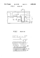
- FIG. 1 is a cross sectional view showing one memory cell of a dynamic RAM having a trench capacitor.
- the dynamic RAM comprises a semiconductor substrate 101 of, for example p-type, having a trench 102, n-type impurity diffused layers 103 and 104 formed on a main surface of the semiconductor substrate 101, a gate electrode 105 formed on a region sandwiched by the n-type impurity diffused layers 103 and 104 with an insulating film interposed therebetween, an n-type impurity diffused layer 106 formed around the trench 102 and connected to the n-type impurity diffused layer 104 and a capacitor electrode 107 formed of polycrystalline silicon formed on the n-type impurity diffused layer 106 with an insulating film interposed therebetween.
- the n-type impurity diffused layer 106, the capacitor electrode 107 and the insulating film interposed therebetween constitute a trench capacitor.
- the width W and the depth D (see FIG. 1) of the trench in a highly integrated memory cell are about 1 ⁇ m and several ⁇ m, respectively.
- the capacity of the trench capacitor is a function of the depth of the trench. Therefore, in order to govern the characteristic value of a semiconductor memory device of this type, the depth of the trench must be precisely measured in a non-destructive and non-contact manner during manufacture.
- the depth of a trench in a non-destructive or non-contact manner include: the wavelength spectral method and the interference spectral method.
- a microlevel difference at a step portion of a sample surface is measured by detecting spectrum of light reflected from the sample's surface, as will be described later.
- the former method employs a means for detecting an interference effect.
- the detecting means is a spectrophotometry means comprising a spectroscope such as a prism, diffraction grating, or the like.
- a spectrophotometry means comprising a spectroscope such as a prism, diffraction grating, or the like.
- the latter method employs a detecting means which spectrophotometry is a means comprising an interferometer.
- FIG. 2 illustrates the conventional measuring methods.
- a micro-trench 36 for forming a trench capacitor is formed on a surface 16A of a sample 16 of a silicon wafer, for example.
- Visible white light L 1 for example, impinges upon the surface 16a in a direction which is substantially perpendicular to the sample surface 16A.
- the visible white light L 1 is reflected by a flat surface (upper portion) of the sample surface 16A and from the bottom of the trench 36 (lower portion). Consequently, a phase difference corresponding to the depth of the trench is generated between the light L 21 reflected from the flat surface of the sample surface 16A and the light L 22 reflected from the bottom of the trench 36.
- the amplitude of the reflected light varies depending on the wavelength, of the light thereby generating an interferenced light.
- FIG. 3A The results of measuring the spectral intensity of such reflected light L 2 is shown FIG. 3A.
- the results shown in FIG. 3A occur when the proportion of the area occupied by the trench in the measured region of the surface is relatively large.
- the intensity distribution of the spectrum changes as a function of to the wavelength ⁇ .
- the distance H between the wave crests of the change corresponds to the depth D of the trench 36.
- FIG. 4 schematically illustrates a principle useful in measuring the thickness of a thin film.
- A denotes an air layer
- B denotes a single layer film
- C denotes a substrate, having reflectances of n 2 , n 1 and n 0 , respectively. Lines with arrows show the direction of passing light. Although as a practical matter the light does not always impinge vertically, the reflectance
- shown in the above equation (1) is a function of sin 2 ⁇ /2. Therefore, the wave crests and wave troughs of the
- FIG. 5 is a graph in which the x axis represents the wavelength while the y axis represents
- the following equations are satisfied: ##EQU1##
- the thickness of the film can be measured from the number of peaks x in a certain wavelength range of and from the reflectance of the film to be measured.
- the depth of a trench can be measured when the thickness of the film is replaced with the depth of the trench.
- FIG. 5 corresponds to FIGS. 3A and 3B.
- the total of the bottom area of trenches is in most cases less than 10% of the area of the region to be measured. If such sample is measured by a conventional method, a large portion of the reflected light will be regularly reflected from a flat portion of the sample surface 16A and not from the trench. Therefore, the proportion of the interferenced light derived from the microlevel difference to the total reflected light becomes extremely small. Consequently, when the light reflected from such sample surface is spectrally analyzed, the average intensity (the average of intensity at each wavelength) is high, and the amplitude (the intensity difference between a wave crest and a wave trough) is small as shown in FIG. 3B.
- a portion of a substrate surface which has an actual pattern (for example a pattern used as a trench capacitor) is replaced with a test portion which has a trench pattern in which the trench is proportionately large.
- the test pattern is measured by the above described method.
- the depth of the trench in the actual pattern is then estimated based on the result.
- this method comprises the following problems. Namely, since a test pattern which is not used as an actual device is formed on the silicon wafer surface, the total surface area of the wafer is unnecessarily increased. Thus, this method is particularly undesirable for forming a highly integrated semiconductor device.
- the areas occupied by the trench in the test pattern and in the actual pattern are not accurately proportional to each other, the depth of
- the trenches in both patterns are liable to differ from each other in the manufacturing process. Consequently, even if the depth of the trench in the test pattern is precisely measured, the depth of the trench in the actual pattern cannot always be precisely measured based on the result of the measurement of the test pattern.
- an object of the present invention is to provide a method of and an apparatus for precisely measuring a microlevel difference even if the density of concave portions relative to convex portions formed on a sample surface is low.
- Another object of the present invention is to provide a method of and an apparatus for measuring a microlevel difference without employing a complicated apparatus.
- a further object of the present invention is to provide an apparatus which is capable of providing signals with less noise and in a simple structure.
- a still further object of the present invention is to provide an apparatus difference which can be readily incorporated with a general metallurgical microscope to form a unit.
- a still further object of the present invention is to provide a method of and an apparatus for precisely measuring the depth of a trench of a trench capacitor.
- the above described objects of the present invention can be attained by an apparatus for measuring the distance between a main surface and a second surface.
- the apparatus includes means for receiving a main surface and a second surface; a light source for illuminating the main surface and the second surface; an optical system for condensing a first component of light which is regularly reflected from the main surface and a second component of interferenced light which is reflected from the main surface and the second surface; and reducing means for reducing the first component relative to the second component.
- the above-described objects of the invention can also be attained by a method of measuring the distance between a main surface and a second surface.
- the method includes placing a sample on a stage (the sample includes a main surface and a second surface); illuminating the sample; reflecting a first component of light from the main surfaces (the first component includes substantially no interference); reflecting a second component of light from the main surface and the second surface (the second component is interfered and the interference corresponds to the distance between the main surface and the second surface); condensing the first and second components; and reducing the first component relative to the second component.
- the above described objects of the invention can also be attained by a system for measuring a very small dimension between a main surface and a second surface.
- the system includes means for illuminating a main surface and a second surface to reflect light from the surfaces (the surfaces are separated by a very small dimension); means for analyzing interferenced light reflected from the surfaces to measure the very small dimension; and means for reducing a component of the light reflected from the surfaces to increase the contrast of the analyzed light and to enhance the measurement of the very small dimension.
- the component comprises the above described components, the proportion of the second reflected light component to the total reflected light is increased, and a signal will be produced for detecting the microlevel difference. Therefore, an apparatus can be provided which is capable of precisely measuring a microlevel difference even if the density of the concave portions or convex portions is low.
- the means for reducing the first reflected light component comprises a means for intercepting the first reflected light component.
- a measuring apparatus which is capable of obtaining signals for measuring a microlevel difference without complicated apparatuses.
- the illuminating light impinges on the main surface of the sample almost vertically; the first reflected light component is almost vertically reflected from the main surface of the sample; the second reflected light component is reflected from the main surface of the sample in arbitrary directions; the condensing optical system comprises an optical axis; and the light intercepting means intercepts light near the optical axis of the condensing optical system.
- an apparatus for measuring a microlevel difference can be provided which is capable of obtaining signals with less noise difference and in a simple structure.
- the light intercepting means comprises a glass mask having an intercepting portion formed at the center and transmissive portions formed on portions other than the light intercepting portion; and a half mirror provided between the glass mask and the condensing optical system for irradiating light from the light source onto the main surface of the sample and for bringing the reflected light to the glass mask.
- the whole apparatus can be readily incoroorated with a general metallurgical microscope.
- the apparatus comprises the above described components, a half mirror for irradiating the sample surface and a glass mask for intercepting that light reflected from the main surface are provided independent from each other. Therefore, an apparatus is provided wherein the sample surface can be sufficiently illuminated and, at the same time, signals for detecting microlevel difference can be obtained.
- a method for measuring a microlevel difference comprises the steps of: placing a sample on a stage, the sample having a portion with a microlevel difference formed on a main surface thereof; illuminating the main surface of the sample by the light from a light source; reflecting a first reflected light component by interfering reflected lights corresponding to the microlevel difference; reflecting a second reflected light component by reflecting light only from the main surface of the sample, the second component comprising no interferenced light; condensing reflected light including the first and second reflected light components; and reducing the first reflected light component relative to the second reflected light component out of the condensed reflected light.
- the condenser optical system comprises an optical axis
- the step of reducing the first reflected light component relative to the second reflected light component reflected light comprises a step of intercepting the first component by intercepting light near the optical axis of the condenser optical system.
- the method comprises the above described steps, the first reflected light component can be readily removed. Therefore, a method capable of readily measuring a microlevel difference can be provided.
- FIG. 1 is a cross sectional view of a DRAM which is an example of an object having a microlevel difference which can be measured by the present invention
- FIG. 2 illustrates a conventional principle of measuring a microlevel difference
- FIG. 3A shows spectral intensity when reflected light comprises a large proportion of signals
- FIG. 3B shows spectral intensity where reflected light comprises a small proportion of signals
- FIG. 4 illustrate a method of measuring thickness of a thin film
- FIG. 5 shows spectral intensity of reflected light to illustrate the method of FIG. 5.
- FIG. 6A illustrated an apparatus for; measuring microlevel difference in accordance with the present invention
- FIG. 6B is a cross sectional view taken along the line VIB--VIB of FIG. 6A;
- FIG. 7 shows a general metallurgical microscope within which the present invention is incorporated
- FIG. 8 shows a preferred actual application of the present invention.
- FIGS. 9A and 9B show spectral distribution of diffracted light entering a spectroscope in accordance with the first embodiment.
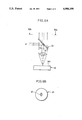
- FIGS. 6A and 6B are schematic diagrams showing a main portion of a measuring apparatus in accordance with a first embodiment of the present invention.
- FIG. 7 is a schematic diagram of the whole structure of the apparatus.
- the apparatus comprises a common metallurgical microscope 2, spectrophotometry means consisting of a spectroscope 4, and a data processing portion 6.
- a metallurgical microscope 2 comprises a light source 8 and an optical system including a special mirror 40, an image forming lens 18, an objective lens 12, etc.
- the spectroscope 4 comprises a field diaphragm 30, a shutter 34, an apertured diaphragm 35, a concave surface diffraction grating 22, and a linear image sensor (hereinafter referred to as CCD) 24.
- the data processing portion 6 comprises a CPU, a keyboard and a CRT 26.
- Visible white light emitted from the light source 8 is reflected by the special mirror 40, passes through an objective lens 12, which will be described later, reaches a surface of a sample 16 such as a silicon wafer set on a stage 14 and is reflected by the surface of the sample.
- the reflected light passes back through the objective lens 12 and impinges on an impinging pin hole 20 of the spectroscope 4 via the special mirror 40, the image forming lens 18 etc.
- the impinging pin hole 20 is arranged on the optical axis at a position where the image of a sample placed on the stage is formed. Therefore, light emitted from approximately a single point of the sample surface passes through the impinging pin hole 20 to reach the concave diffraction grating 22.
- the concave diffraction grating 22 spectrally analyzes the to light received thereon.
- the resulting spectrum is converted into electrical signals by photoelectric converting means of the CCD 24.
- the electric signals are applied to the data processing portion 6.
- the data are arithmetically processed appropriately to determine the microlevel difference, with the result being applied to the CRT 26 or to a printer 28.
- the light source 8 comprises a white illuminating lamp which irradiates visible white light.
- the objective lens 12 has the function of condensing light reflected from the same surface as well as the function of irradiating light from the source 8 onto the sample surface.
- the aperture of the diaphragm 35 is smaller than that of the objective lens 12. Consequently, the expansion of a bundle of rays of visible white light emitted from the objective lens 12 is less than that of the bundle of rays of reflected light entering the objective lens. More specifically, the diameter of the apertured diaphragm 35 is preferably adjusted to be 3 mm.
- FIG. 6B is a plan view of the special mirror 40 viewed from section line VIB--VIB of FIG. 6A. Only the central portion of the special mirror 40 has a mirrored surface 42. Therefore, the central portion of the special mirror 40 has light intercepting characteristics. More specifically, the special mirror 40 comprises a regular reflecting region 42 formed by an aluminum film or the like on the central portion of a glass plate. The special mirror 40 is positioned at an angle of 45° to the incidental light in order to reflect the visible white light L 4 from the source vertically.
- the mirrored surface 42 is elliptical with a length of about 4.2 mm and a breadth of 3 mm. Thus, when the mirrored surface 42 is viewed from the irradiating direction it will appear circular. Portions of the special mirror 40 other than the mirrored surface 42 are transmissive.
- the special mirror 40 may be a half mirror.
- the objective lens 12 is preferably designed such that the focal distance thereof is 9 mm and the optical axis thereof is substantially vertical to the sample surface.
- the visible white light L 4 emitted from the light source is reflected by the mirrored surface 42 to enter the objective lens 12 and is converged to irradiate a small area of the sample surface 16A including the trench 36 and an area of surface 16A including the trench 36 and area of surface 16A immediately surrounding the trench 36.
- a portion of the visible white light L 4 which impinges on the sample surface 16A is regularly reflected.
- the visible white light L 4 impinging in the vicinity of the trench 36 is diffracted and returned to the objective lens 12.
- the light regularly reflected from the sample surface 16A passes near the center of the optical axis of the objective lens 12 to reach the special mirror 40. Since the mirrored surface 42 is formed on that portion where the regularly reflected light enters, the regularly reflected light is intercepted in this region. Therefore, the regularly reflected light does not proceed beyond the mirror (to the spectroscope 4).
- Diffracted light returning from the sample surface 16A is widely distributed relative to the regularly reflected light.
- the diffracted light passes through the special mirror 40 with only a few portions thereof intercepted by the mirrored 42.
- the diffracted light which passes through the special mirror 40 is converged by the image forming lens 18 to enter the impinging pin hole 20 of the spectroscope 4.
- the special mirror 40 serves as both a light intercepting means and as a directing means which reflects the visible white light from the light source 8 such that the light irradiates the sample surface substantially vertically. Compared with a case where the light intercepting means and the directing means are provided separately, the number of parts in the first embodiment reduced.
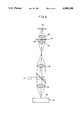
- FIG. 8 is a schematic diagram showing a main portion of a second embodiment of the present invention.
- the special mirror 40 is replaced with a half mirror 10 and a glass mask 46 having the central portion screened.
- the special mirror 40 for performing a light intercepting function.
- the rear focus point of an objective lens is either located in the objective lens or to the rear of the lens. If the glass mask 46 were set at the rear focus point of the objective lens, the illuminating light (visible white light) would itself be intercepted before entering the objective lens. Therefore, the illuminating light could not be used to irradiate the sample surface. Also, the glass mask 46 cannot be set at a position which is in a conjugate relation with the rear focus point of the objective lens 12. The reason for this is that such a position would be higher than the impinging pin hole of the spectroscope. Therefore, in the second embodiment, a lens system 44, 50 is provided in order to set the glass mask at an appropriate position.
- a lens unit 44 is placed behind the rear focus point of the image forming lens 18. Consequently, the image forming position of the rear focus point of the objective lens is set and the glass mask 46 is set at the position.
- the glass mask 46 is a fully-transmissive glass plate, with a light intercepting film 48 (preferably having a diameter of 1 mm) formed at the central portion thereof.
- a lens unit 50 is arranged above the glass mask 46 and light converged by the lens unit 50 enters the impinging pin hole 20 of the spectroscope 4.
- the diameter of the objective lens 12 is 10 mm
- the focal distance thereof is 9 mm
- the focal distance of the image forming lens 18 is 180 mm
- the focal distance of the lens unit 44 is 50 mm
- the focal distance of the lens unit 50 is 15 mm.
- the visible white light L 4 (adjusted by the apertured diaphragm such that the diameter of the bundle of rays at the position of the apertured diaphragm 35 is about 3 mm) is reflected vertically downwardly by the half mirror 10 to reach the sample surface 16 1 through the objective lens 12.
- the regularly reflected light and the diffracted light from the sample surface 16A reach the glass mask 46 through the objective lens 12, the half mirror 10, the image forming lens 18 and the lens unit 44.
- the regularly reflected light reaching the glass mask 46 is intercepted by the light intercepting film 48 of the glass mask 46.
- the diffracted light is relatively widely distributed around the regularly reflected light and therefore passes through the transmissive portion around the light intercepting film 48 and enters the impinging pin hole 20 through the lens 50.
- the second embodiment a common half mirror is used instead of the special mirror 40 of the first embodiment. Therefore, compared with the first embodiment, the second embodiment is more easily manufactured. In the second embodiment, since the light to the spectroscope passes through the half mirror, the light amount is slightly decreased. In the first embodiment, the amount of light to the spectroscope is not decreased.
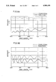
- FIGS. 9A and 9B are graphs showing the spectral distribution obtained by spectrally analyzing the diffracted light entering the spectroscope in accordance with the first embodiment, compared with the prior art.
- the spectral distribution of the embodiment is denoted by a solid line while that of the prior art is shown by a dotted line.
- FIG. 9A is a spectral distribution of a sample in which the diameter of the opening of a hole is 1.5 ⁇ m, the depth of the same is 4 ⁇ m and the proportion of the area occupied by the hole is 8%.
- FIG. 9B is the spectral distribution of a sample having holes of the same shape and the proportion of the area occupied by the hole is 40%.
- the proportion of the diffracted light at the step portion of the sample surface to the total amount of the reflected light is high, a spectrum of light can be measured in which the influence of the interferenced light is larger than in the spectrum of the prior art.
- the spectrum has such characteristics that the amplitude, which is the intensity difference between the wave crest and the wave trough, is not minimized and the average intensity, which is the average of intensity at each wavelength, is suppressed. By suppressing the average intensity, a spectrum having high contrast can be obtained.
- the present invention can employ any light source provided it irradiates light having continuous spectrum.
- the range of wavelengths is not limited to the visible range.
- the light source need not irradiate light having continuous spectrum simultaneously. For example, it may irradiate light whose wavelength changes continuously.
- a spectroscope 4 comprising a concave diffraction grating 22 is employed.
- a prism may be used instead of the concave diffraction grating 22.
- the spectrum may be measured by an interference spectral method instead of the wavelength spectral method.
- the irradiation of white light onto the sample surface should be approximately vertical to the sample surface, however, it need not be completely vertical. However, the bottom of the trench or concave portion must be irradiated.
- the above described apparatus can be used to measure the height of a convex portion i.e., a portion which projects from a flat surface.
- a special mirror having an intercepting portion at the center or the like intercepts reflected light which is simply regularly reflected from the surface of the sample near the optical axis thereof. Meanwhile, interfered light reflected at the portions having microlevel difference, enters a spectroscope through the peripheral portion of the special mirror and the like. Therefore, the proportion of the light which is regularly reflected from the sample surface (which would be noise) to the diffracted light (non-regularly reflected light which will be the signal for measuring the microlevel difference) is considerably decreased. Namely, the signal to noise ratio in measurement is considerably improved. Consequently, an apparatus is provided which can precisely measure a microlevel difference even if the density of the concave portions formed on a sample surface is low.
Landscapes
- Physics & Mathematics (AREA)
- General Physics & Mathematics (AREA)
- Length Measuring Devices By Optical Means (AREA)
Abstract
Description
|R1|.sup.2 =1-4n.sub.0 n.sub.1.sup.2 n.sub.2 /{n.sub.1.sup.2 (n.sub.0 +n.sub.1).sup.2 -(n.sub.1.sup.2 -n.sub.2.sup.2).(n.sub.0.sup.2 -n.sub.1.sup.2) sin .sup.2 δ.sub.1 /2}(1)
Claims (2)
Applications Claiming Priority (2)
| Application Number | Priority Date | Filing Date | Title |
|---|---|---|---|
| JP62155125A JPH0617774B2 (en) | 1987-06-22 | 1987-06-22 | Micro height difference measuring device |
| JP62-155125 | 1987-06-22 |
Publications (1)
| Publication Number | Publication Date |
|---|---|
| US4988198A true US4988198A (en) | 1991-01-29 |
Family
ID=15599104
Family Applications (1)
| Application Number | Title | Priority Date | Filing Date |
|---|---|---|---|
| US07/210,033 Expired - Fee Related US4988198A (en) | 1987-06-22 | 1988-06-22 | Method and apparatus for measuring microlevel difference |
Country Status (3)
| Country | Link |
|---|---|
| US (1) | US4988198A (en) |
| JP (1) | JPH0617774B2 (en) |
| KR (1) | KR920004751B1 (en) |
Cited By (11)
| Publication number | Priority date | Publication date | Assignee | Title |
|---|---|---|---|---|
| EP0505852A3 (en) * | 1991-03-28 | 1993-09-29 | Firma Carl Zeiss | Device to interferometrically measure the thickness of a transparent layer |
| EP0577399A3 (en) * | 1992-06-29 | 1995-05-10 | Hughes Aircraft Co | Apparatus and method for performing thin film layer thickness metrology on a thin film layer having shape deformations and local slope variations. |
| US5440141A (en) * | 1993-08-20 | 1995-08-08 | Dainippon Screen Mfg. Co., Ltd. | Method of measuring a thickness of a multilayered sample using ultraviolet light and light with wavelengths longer than ultraviolet |
| WO1996002807A1 (en) * | 1994-07-13 | 1996-02-01 | Leonhard Kurz Gmbh & Co. | Process for measuring the depth of a microstructure |
| FR2737560A1 (en) * | 1995-08-02 | 1997-02-07 | Sofie Instr | METHOD AND DEVICE FOR QUANTIFYING IN SITU, BY REFLECTOMETRY, THE MORPHOLOGY OF A LOCALIZED AREA DURING THE ENGRAVING OF THE SURFACE LAYER OF A THIN-LAYER STRUCTURE |
| US5648849A (en) * | 1994-04-05 | 1997-07-15 | Sofie | Method of and device for in situ real time quantification of the morphology and thickness of a localized area of a surface layer of a thin layer structure during treatment of the latter |
| WO1998058400A3 (en) * | 1997-06-17 | 1999-04-01 | Luxtron Corp | Liquid etch endpoint detection and process metrology |
| US20030222049A1 (en) * | 1999-09-30 | 2003-12-04 | Lam Research | Methods and apparatuses for trench depth detection and control |
| US20040185582A1 (en) * | 2003-03-19 | 2004-09-23 | Kueny Andrew Weeks | System and method for in-situ monitor and control of film thickness and trench depth |
| CN102620666A (en) * | 2012-03-29 | 2012-08-01 | 吴周令 | Detecting system for semiconductor wafer thickness and detecting method thereof |
| US20150323470A1 (en) * | 2014-05-07 | 2015-11-12 | Boe Technology Group Co., Ltd. | Detection device and method |
Families Citing this family (4)
| Publication number | Priority date | Publication date | Assignee | Title |
|---|---|---|---|---|
| JP2006258769A (en) * | 2005-03-18 | 2006-09-28 | Toshiba Corp | Photodetector |
| JP2007225392A (en) * | 2006-02-22 | 2007-09-06 | Spectratech Inc | Optical interference device |
| JP5172203B2 (en) * | 2007-05-16 | 2013-03-27 | 大塚電子株式会社 | Optical characteristic measuring apparatus and measuring method |
| JP2011122894A (en) * | 2009-12-09 | 2011-06-23 | Disco Abrasive Syst Ltd | Apparatus for measuring workpiece held at chuck table and laser beam machine |
Citations (5)
| Publication number | Priority date | Publication date | Assignee | Title |
|---|---|---|---|---|
| US3796497A (en) * | 1971-12-01 | 1974-03-12 | Ibm | Optical alignment method and apparatus |
| US4254337A (en) * | 1978-09-04 | 1981-03-03 | Asahi-Dow Limited | Infrared interference type film thickness measuring method and instrument therefor |
| JPS61107104A (en) * | 1984-10-31 | 1986-05-26 | Hitachi Ltd | Fine pattern depth measurement method and device |
| US4615620A (en) * | 1983-12-26 | 1986-10-07 | Hitachi, Ltd. | Apparatus for measuring the depth of fine engraved patterns |
| US4744660A (en) * | 1985-04-12 | 1988-05-17 | Hitachi, Ltd. | Apparatus for measuring difference in shallow level |
-
1987
- 1987-06-22 JP JP62155125A patent/JPH0617774B2/en not_active Expired - Lifetime
-
1988
- 1988-06-22 KR KR1019880007519A patent/KR920004751B1/en not_active Expired
- 1988-06-22 US US07/210,033 patent/US4988198A/en not_active Expired - Fee Related
Patent Citations (5)
| Publication number | Priority date | Publication date | Assignee | Title |
|---|---|---|---|---|
| US3796497A (en) * | 1971-12-01 | 1974-03-12 | Ibm | Optical alignment method and apparatus |
| US4254337A (en) * | 1978-09-04 | 1981-03-03 | Asahi-Dow Limited | Infrared interference type film thickness measuring method and instrument therefor |
| US4615620A (en) * | 1983-12-26 | 1986-10-07 | Hitachi, Ltd. | Apparatus for measuring the depth of fine engraved patterns |
| JPS61107104A (en) * | 1984-10-31 | 1986-05-26 | Hitachi Ltd | Fine pattern depth measurement method and device |
| US4744660A (en) * | 1985-04-12 | 1988-05-17 | Hitachi, Ltd. | Apparatus for measuring difference in shallow level |
Cited By (16)
| Publication number | Priority date | Publication date | Assignee | Title |
|---|---|---|---|---|
| EP0505852A3 (en) * | 1991-03-28 | 1993-09-29 | Firma Carl Zeiss | Device to interferometrically measure the thickness of a transparent layer |
| EP0577399A3 (en) * | 1992-06-29 | 1995-05-10 | Hughes Aircraft Co | Apparatus and method for performing thin film layer thickness metrology on a thin film layer having shape deformations and local slope variations. |
| US5440141A (en) * | 1993-08-20 | 1995-08-08 | Dainippon Screen Mfg. Co., Ltd. | Method of measuring a thickness of a multilayered sample using ultraviolet light and light with wavelengths longer than ultraviolet |
| US5648849A (en) * | 1994-04-05 | 1997-07-15 | Sofie | Method of and device for in situ real time quantification of the morphology and thickness of a localized area of a surface layer of a thin layer structure during treatment of the latter |
| WO1996002807A1 (en) * | 1994-07-13 | 1996-02-01 | Leonhard Kurz Gmbh & Co. | Process for measuring the depth of a microstructure |
| FR2737560A1 (en) * | 1995-08-02 | 1997-02-07 | Sofie Instr | METHOD AND DEVICE FOR QUANTIFYING IN SITU, BY REFLECTOMETRY, THE MORPHOLOGY OF A LOCALIZED AREA DURING THE ENGRAVING OF THE SURFACE LAYER OF A THIN-LAYER STRUCTURE |
| US5748296A (en) * | 1995-08-02 | 1998-05-05 | Sofie Instruments | Method and device for in situ quantification, by reflectometry, of the morphology of a localized region during etching of the surface layer of a thin-film structure |
| US6406641B1 (en) | 1997-06-17 | 2002-06-18 | Luxtron Corporation | Liquid etch endpoint detection and process metrology |
| WO1998058400A3 (en) * | 1997-06-17 | 1999-04-01 | Luxtron Corp | Liquid etch endpoint detection and process metrology |
| US20030222049A1 (en) * | 1999-09-30 | 2003-12-04 | Lam Research | Methods and apparatuses for trench depth detection and control |
| US6878301B2 (en) * | 1999-09-30 | 2005-04-12 | Lam Research | Methods and apparatuses for trench depth detection and control |
| US20040185582A1 (en) * | 2003-03-19 | 2004-09-23 | Kueny Andrew Weeks | System and method for in-situ monitor and control of film thickness and trench depth |
| US7049156B2 (en) | 2003-03-19 | 2006-05-23 | Verity Instruments, Inc. | System and method for in-situ monitor and control of film thickness and trench depth |
| CN102620666A (en) * | 2012-03-29 | 2012-08-01 | 吴周令 | Detecting system for semiconductor wafer thickness and detecting method thereof |
| US20150323470A1 (en) * | 2014-05-07 | 2015-11-12 | Boe Technology Group Co., Ltd. | Detection device and method |
| US9435634B2 (en) * | 2014-05-07 | 2016-09-06 | Boe Technology Group Co., Ltd. | Detection device and method |
Also Published As
| Publication number | Publication date |
|---|---|
| JPH0617774B2 (en) | 1994-03-09 |
| KR920004751B1 (en) | 1992-06-15 |
| KR890000876A (en) | 1989-03-17 |
| JPS63317706A (en) | 1988-12-26 |
Similar Documents
| Publication | Publication Date | Title |
|---|---|---|
| US4988198A (en) | Method and apparatus for measuring microlevel difference | |
| US5717485A (en) | Foreign substance inspection apparatus | |
| US5856871A (en) | Film thickness mapping using interferometric spectral imaging | |
| JP2648440B2 (en) | Apparatus and method for metrologically processing the thickness of a thin film layer on a thin film layer having a deformed shape and a partially changed slope | |
| US7705974B2 (en) | Metrology system with spectroscopic ellipsometer and photoacoustic measurements | |
| US8319975B2 (en) | Methods and apparatus for wavefront manipulations and improved 3-D measurements | |
| US5333049A (en) | Apparatus and method for interferometrically measuring the thickness of thin films using full aperture irradiation | |
| US7177030B2 (en) | Determination of thin film topography | |
| KR100898963B1 (en) | Inspection system for two-dimensional imaging with line light spots | |
| US20050174583A1 (en) | Method and apparatus for high-speed thickness mapping of patterned thin films | |
| JPH0718806B2 (en) | Optical internal inspection support device and method | |
| EP0650030A2 (en) | Apparatus for and method of evaluating multilayer thin films | |
| US4815849A (en) | Spectrometer using concave holographic diffraction grating | |
| CN1225720A (en) | Optical measurement | |
| US7321433B2 (en) | Method and apparatus for optically measuring the topography of nearly planar periodic structures | |
| US20020057437A1 (en) | Apparatus and method for enabling high resolution film thickness and thickness-uniformity measurements | |
| KR101398835B1 (en) | Spectral interferometer using comb generation and detection technique for real-time profile measurement | |
| JP2533514B2 (en) | Depth / thickness measuring device | |
| US20050168753A1 (en) | Optical measurement of device features using interferometric illumination | |
| JPH0665963B2 (en) | Fine groove depth measuring device | |
| US11703461B2 (en) | Optical sensor for surface inspection and metrology | |
| US20190170505A1 (en) | Measurement of surface topography of a work-piece | |
| USRE33424E (en) | Apparatus and method for measuring the depth of fine engraved patterns | |
| US7369235B1 (en) | Method and system for measuring deep trenches in silicon | |
| JPH0527256B2 (en) |
Legal Events
| Date | Code | Title | Description |
|---|---|---|---|
| AS | Assignment |
Owner name: DAINIPPON SCREEN MFG., CO., LTD., 1-1 TENJINKITAMA Free format text: ASSIGNMENT OF ASSIGNORS INTEREST.;ASSIGNOR:KONDO, NORIYUKI;REEL/FRAME:004911/0686 Effective date: 19880608 Owner name: DAINIPPON SCREEN MFG., CO., LTD.,JAPAN Free format text: ASSIGNMENT OF ASSIGNORS INTEREST;ASSIGNOR:KONDO, NORIYUKI;REEL/FRAME:004911/0686 Effective date: 19880608 |
|
| FEPP | Fee payment procedure |
Free format text: PAYOR NUMBER ASSIGNED (ORIGINAL EVENT CODE: ASPN); ENTITY STATUS OF PATENT OWNER: LARGE ENTITY |
|
| FPAY | Fee payment |
Year of fee payment: 4 |
|
| FEPP | Fee payment procedure |
Free format text: PAYER NUMBER DE-ASSIGNED (ORIGINAL EVENT CODE: RMPN); ENTITY STATUS OF PATENT OWNER: LARGE ENTITY Free format text: PAYOR NUMBER ASSIGNED (ORIGINAL EVENT CODE: ASPN); ENTITY STATUS OF PATENT OWNER: LARGE ENTITY |
|
| FPAY | Fee payment |
Year of fee payment: 8 |
|
| REMI | Maintenance fee reminder mailed | ||
| LAPS | Lapse for failure to pay maintenance fees | ||
| STCH | Information on status: patent discontinuation |
Free format text: PATENT EXPIRED DUE TO NONPAYMENT OF MAINTENANCE FEES UNDER 37 CFR 1.362 |
|
| FP | Lapsed due to failure to pay maintenance fee |
Effective date: 20030129 |