US4937423A - Method of disconnecting a short-circuited part between mutually opposed electrodes - Google Patents
Method of disconnecting a short-circuited part between mutually opposed electrodes Download PDFInfo
- Publication number
- US4937423A US4937423A US07/231,469 US23146988A US4937423A US 4937423 A US4937423 A US 4937423A US 23146988 A US23146988 A US 23146988A US 4937423 A US4937423 A US 4937423A
- Authority
- US
- United States
- Prior art keywords
- short
- disconnecting
- circuited
- part according
- circuited part
- Prior art date
- Legal status (The legal status is an assumption and is not a legal conclusion. Google has not performed a legal analysis and makes no representation as to the accuracy of the status listed.)
- Expired - Lifetime
Links
- 238000000034 method Methods 0.000 title claims abstract description 32
- 239000000758 substrate Substances 0.000 claims abstract description 34
- 238000009413 insulation Methods 0.000 claims abstract description 7
- VYPSYNLAJGMNEJ-UHFFFAOYSA-N Silicium dioxide Chemical compound O=[Si]=O VYPSYNLAJGMNEJ-UHFFFAOYSA-N 0.000 claims description 19
- GWEVSGVZZGPLCZ-UHFFFAOYSA-N Titan oxide Chemical compound O=[Ti]=O GWEVSGVZZGPLCZ-UHFFFAOYSA-N 0.000 claims description 10
- 229910052681 coesite Inorganic materials 0.000 claims description 10
- 229910052906 cristobalite Inorganic materials 0.000 claims description 10
- 229910052682 stishovite Inorganic materials 0.000 claims description 10
- 229910052905 tridymite Inorganic materials 0.000 claims description 10
- 239000000377 silicon dioxide Substances 0.000 claims description 9
- 229920001721 polyimide Polymers 0.000 claims description 6
- 230000001678 irradiating effect Effects 0.000 claims description 5
- 239000004642 Polyimide Substances 0.000 claims description 4
- 239000004372 Polyvinyl alcohol Substances 0.000 claims description 4
- 229910004446 Ta2 O5 Inorganic materials 0.000 claims description 4
- -1 polyamidoimide Polymers 0.000 claims description 4
- 229920002451 polyvinyl alcohol Polymers 0.000 claims description 4
- 239000004952 Polyamide Substances 0.000 claims description 3
- 238000001704 evaporation Methods 0.000 claims description 3
- 230000008020 evaporation Effects 0.000 claims description 3
- 229920003055 poly(ester-imide) Polymers 0.000 claims description 3
- 229920002647 polyamide Polymers 0.000 claims description 3
- 239000010979 ruby Substances 0.000 claims description 3
- 229910001750 ruby Inorganic materials 0.000 claims description 3
- 239000000463 material Substances 0.000 claims description 2
- 239000004973 liquid crystal related substance Substances 0.000 description 25
- 239000010408 film Substances 0.000 description 21
- 210000004027 cell Anatomy 0.000 description 13
- 239000005262 ferroelectric liquid crystals (FLCs) Substances 0.000 description 13
- 239000011324 bead Substances 0.000 description 8
- 230000008439 repair process Effects 0.000 description 7
- 238000002474 experimental method Methods 0.000 description 6
- 239000011521 glass Substances 0.000 description 4
- 238000010438 heat treatment Methods 0.000 description 4
- KFZMGEQAYNKOFK-UHFFFAOYSA-N Isopropanol Chemical compound CC(C)O KFZMGEQAYNKOFK-UHFFFAOYSA-N 0.000 description 3
- ZOKXTWBITQBERF-UHFFFAOYSA-N Molybdenum Chemical compound [Mo] ZOKXTWBITQBERF-UHFFFAOYSA-N 0.000 description 3
- 230000002950 deficient Effects 0.000 description 3
- 229910052751 metal Inorganic materials 0.000 description 3
- 239000002184 metal Substances 0.000 description 3
- 229910052750 molybdenum Inorganic materials 0.000 description 3
- 239000011733 molybdenum Substances 0.000 description 3
- 239000002245 particle Substances 0.000 description 3
- 239000004840 adhesive resin Substances 0.000 description 2
- 229920006223 adhesive resin Polymers 0.000 description 2
- 238000001816 cooling Methods 0.000 description 2
- 230000007547 defect Effects 0.000 description 2
- 238000010586 diagram Methods 0.000 description 2
- 239000011159 matrix material Substances 0.000 description 2
- 229920003023 plastic Polymers 0.000 description 2
- 239000004033 plastic Substances 0.000 description 2
- LIVNPJMFVYWSIS-UHFFFAOYSA-N silicon monoxide Chemical compound [Si-]#[O+] LIVNPJMFVYWSIS-UHFFFAOYSA-N 0.000 description 2
- 125000006850 spacer group Chemical group 0.000 description 2
- 239000010409 thin film Substances 0.000 description 2
- VYZAMTAEIAYCRO-UHFFFAOYSA-N Chromium Chemical compound [Cr] VYZAMTAEIAYCRO-UHFFFAOYSA-N 0.000 description 1
- RYGMFSIKBFXOCR-UHFFFAOYSA-N Copper Chemical compound [Cu] RYGMFSIKBFXOCR-UHFFFAOYSA-N 0.000 description 1
- 239000004988 Nematic liquid crystal Substances 0.000 description 1
- BQCADISMDOOEFD-UHFFFAOYSA-N Silver Chemical compound [Ag] BQCADISMDOOEFD-UHFFFAOYSA-N 0.000 description 1
- 239000004990 Smectic liquid crystal Substances 0.000 description 1
- YQNPZKUDUWSYQX-UHFFFAOYSA-N [O-2].[In+3].[Mo+4] Chemical compound [O-2].[In+3].[Mo+4] YQNPZKUDUWSYQX-UHFFFAOYSA-N 0.000 description 1
- 230000002411 adverse Effects 0.000 description 1
- 229910045601 alloy Inorganic materials 0.000 description 1
- 239000000956 alloy Substances 0.000 description 1
- 229910052782 aluminium Inorganic materials 0.000 description 1
- XAGFODPZIPBFFR-UHFFFAOYSA-N aluminium Chemical compound [Al] XAGFODPZIPBFFR-UHFFFAOYSA-N 0.000 description 1
- 230000015572 biosynthetic process Effects 0.000 description 1
- 229910052804 chromium Inorganic materials 0.000 description 1
- 239000011651 chromium Substances 0.000 description 1
- 229910052802 copper Inorganic materials 0.000 description 1
- 239000010949 copper Substances 0.000 description 1
- 210000002858 crystal cell Anatomy 0.000 description 1
- 230000007423 decrease Effects 0.000 description 1
- 238000001035 drying Methods 0.000 description 1
- 239000000428 dust Substances 0.000 description 1
- 230000005684 electric field Effects 0.000 description 1
- 229920006332 epoxy adhesive Polymers 0.000 description 1
- 238000005530 etching Methods 0.000 description 1
- 239000004744 fabric Substances 0.000 description 1
- PCHJSUWPFVWCPO-UHFFFAOYSA-N gold Chemical compound [Au] PCHJSUWPFVWCPO-UHFFFAOYSA-N 0.000 description 1
- 229910052737 gold Inorganic materials 0.000 description 1
- 239000010931 gold Substances 0.000 description 1
- 229910003437 indium oxide Inorganic materials 0.000 description 1
- PJXISJQVUVHSOJ-UHFFFAOYSA-N indium(iii) oxide Chemical compound [O-2].[O-2].[O-2].[In+3].[In+3] PJXISJQVUVHSOJ-UHFFFAOYSA-N 0.000 description 1
- AMGQUBHHOARCQH-UHFFFAOYSA-N indium;oxotin Chemical compound [In].[Sn]=O AMGQUBHHOARCQH-UHFFFAOYSA-N 0.000 description 1
- 239000007788 liquid Substances 0.000 description 1
- 238000004519 manufacturing process Methods 0.000 description 1
- 150000002739 metals Chemical class 0.000 description 1
- 230000010355 oscillation Effects 0.000 description 1
- 230000010287 polarization Effects 0.000 description 1
- 229920000728 polyester Polymers 0.000 description 1
- 229920000573 polyethylene Polymers 0.000 description 1
- 229920000136 polysorbate Polymers 0.000 description 1
- 229920005989 resin Polymers 0.000 description 1
- 239000011347 resin Substances 0.000 description 1
- 229910052709 silver Inorganic materials 0.000 description 1
- 239000004332 silver Substances 0.000 description 1
Images


Classifications
-
- G—PHYSICS
- G02—OPTICS
- G02F—OPTICAL DEVICES OR ARRANGEMENTS FOR THE CONTROL OF LIGHT BY MODIFICATION OF THE OPTICAL PROPERTIES OF THE MEDIA OF THE ELEMENTS INVOLVED THEREIN; NON-LINEAR OPTICS; FREQUENCY-CHANGING OF LIGHT; OPTICAL LOGIC ELEMENTS; OPTICAL ANALOGUE/DIGITAL CONVERTERS
- G02F1/00—Devices or arrangements for the control of the intensity, colour, phase, polarisation or direction of light arriving from an independent light source, e.g. switching, gating or modulating; Non-linear optics
- G02F1/01—Devices or arrangements for the control of the intensity, colour, phase, polarisation or direction of light arriving from an independent light source, e.g. switching, gating or modulating; Non-linear optics for the control of the intensity, phase, polarisation or colour
- G02F1/13—Devices or arrangements for the control of the intensity, colour, phase, polarisation or direction of light arriving from an independent light source, e.g. switching, gating or modulating; Non-linear optics for the control of the intensity, phase, polarisation or colour based on liquid crystals, e.g. single liquid crystal display cells
- G02F1/133—Constructional arrangements; Operation of liquid crystal cells; Circuit arrangements
- G02F1/1333—Constructional arrangements; Manufacturing methods
- G02F1/1343—Electrodes
- G02F1/13439—Electrodes characterised by their electrical, optical, physical properties; materials therefor; method of making
Definitions
- the present invention relates to a method of repairing a liquid crystal display panel, and more particularly to a method of repairing a ferroelectric liquid crystal display panel, that repairs a short circuit occurred between upper and lower electrodes owing to inclusion of a foreign matter in a cell.
- liquid crystal display panels Since publication of twisted-nematic liquid crystals (TN liquid crystals) in "Applied Physics Letters", Vol. 18, No. 4, pp.127-128, by Shadt and W. Helfrich in 1971, liquid crystal display panels have made rapid progress, but recent trend in development of goods is shifting from original numerical display panels using segment electrodes to character display panels using a dot matrix. Particularly in recent years demanded is commercialization of liquid crystal display panels having a picture element of a large capacity and capable of answering for the display screens of word processors or personal computers and the display screens of televisions.
- TN liquid crystals twisted-nematic liquid crystals
- any short-circuited part present at the site at which scanning lines and data lines cross may be identified by a vieWer as a line defect (non-switching line) having a shape of a cross formed by the scanning line and signal line at the short-circuited part, resulting in a loWering of display quality.
- an object of the present invention is to provide a method of repairing a liquid crystal display panel that can solve the above problems, and to provide a liquid crystal display panel whose display quality has been thereby improved.
- Another object of the present invention is to provide a process of preparing a liquid crystal display panel that can achieve an improved yield in the manufacture of liquid crystal display panels.
- a method of disconnecting a short-circuited part between upper and lower electrodes comprising the steps of;
- FIG. 1A is a plan view illustrating a display panel having been not repaired
- FIG. 1B is an enlarged plan view of a short-circuited site thereof
- FIG. 1C is a cross section along the line A-A';
- FIG. 2 is a block diagram of a repair apparatus used in the method of the present invention.
- FIG. 3A is a plan view illustrating the method of the present invention, and FIG. 3B is a cross section thereof;
- FIG. 4A is a plan view illustrating a display panel having been repaired according to the present invention, and FIG. 4B is a cross section thereof;
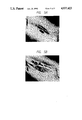
- FIG. 5A is an electron microscope photograph showing a state of metal structure on an upper substrate after repairment
- FIG. 5B is an electron microscope photograph showing a state of metal structure on a lower substrate after that.
- FIG. 1A is a plan view illustrating a liquid crystal display panel 11, and FIG. 1B is an enlarged plan view of the part X in FIG. 1A.
- FIG. 1C is a cross section along the line A-A' in FIG. 1B.
- the liquid crystal display panel 11 illustrated in FIG. 1 is provided with ferroelectric liquid crystal 16 between an upper substrate 13 provided with a transparent common electrode (a terminal) 12 (that functions, for example, as a scanning electrode at the time of multiplexing drive) and a lower substrate 15 provided with transparent opposed electrodes (a terminal) 14 (that functions, for example, as a signal electrode at the time of multiplexing drive).
- a non switching scanning line ⁇ and a non-switching signal line ⁇ is identified in a display screen by a viewer.
- Line N in FIG. 1B corresponds to a line on which no mutually opposed electrodes are formed.
- the position of a polarization axis of a polarizer and an analyzer is so set that the liquid crystal alignment on the line N may be in the dark state when the liquid crystal is placed between the polarizer and the analyzer.
- the transparent common electrode 12 and the transparent opposed electrodes 14 are provided with electrically connected low-resistance lines 17b and 17a, respectively.
- This low-resistance lines 17b and 17a can be formed using metals such as silver, copper, gold, aluminum, chromium and molybdenum or alloys of any of these and may have a film thickness in the range of from 500 angstroms to 5,000 angstroms, preferably from 1,000 angstroms to 3,000 angstroms.
- the line width thereof may preferably be set in the range of from 10 ⁇ m to 50 ⁇ m.
- the defective line ⁇ - ⁇ mentioned above which appeared in the display screen is a site corresponding to a crossing part of the defective line ⁇ - ⁇ and caused by a short circuit occurred between a transparent common electrode 12a and a transparent signal electrode 14a as illustrated in FIG. 1C.
- a foreign matter 18 as exemplified by dust and resin is included between the lower substrate 15 and transparent opposed electrode 14a, thus producing a convex on the transparent opposed electrode 14a, which causes a short circuit in contact with the transparent common electrode 12a.
- the causes of the short circuit may also include a state in which a conductive particle is held between the transparent common electrode 12 and transparent opposed electrode 14.
- Such a short-circuited part can be detected by actuating terminals 19a and 19b of a circuit tester 19.
- FIG. 2 is a block diagram illustrating a repair apparatus used in the method of the present invention.
- the numeral 21 denotes a microscope; 22, a viewer; 23, an objective lens; 24, a slit; 25, a pilot light source: 26, a beam expander; 27, a laser beam; and 28, a laser beam generator.
- &he short-circuited si&e existing in the ferroelectric liquid crystal display panel 11 is detected by the microscope 21, and thereafter the positioning of the site to which the laser beam is irradiated and the spot-setting of the laser beam 27 can be carried out by irradiating light from the pilot light source 28.
- the pilot light source 25 On the light path from the pilot light source 25 to the ferroelectric liquid crystal display panel 11, provided are half mirrors 20a and 20b, and a slit 24 that controls the X-axis and Y-axis of the laser-beam irradiated part 31 and narrows the beam width.
- the laser beam 27 from the laser beam generator 28 is, after being expanded in its width through the beam expander 26, reflected by half mirrors 20b and 20a, and irradiated on the ferroelectric liquid crystal display panel.
- irradiating the laser beam 27 as illustrated in FIG. 3 enables formation of an insulation disconnected part 41 at which the short-circuited site is disconnected from the transparent common electrode 12a and transparent opposed electrode 14a as illustrated in FIG. 4.
- the laser beam 27 used as the laser beam 27 are a YAG laser beam, a ruby laser beam and a CO 2 laser beam, and the YAG laser (oscillation wavelength: 1.06 ⁇ m) may preferably be used in instances in which the transparent&electrodes 12 and 14 are formed with ITO (indium tin-oxide) and also the low resistance lines 17a and 17b are formed with molybdenum.
- the beam spot of this laser beam 27 can be arbitrarily set, but may generally range from 1 ⁇ m to 100 ⁇ m, preferably from 1 ⁇ m to 10 ⁇ m in approximation.
- Laser power may be from 0.1 mJ/pulse to 10 mJ/pulse in approximation, and its pulse width may be from 1 to 100 nsec in approximation.
- the insulation- disconnected part 41 is required to be formed so that the transparent common electrode 12 and &he transparent opposed electrode 14 may not undergo any insulation disconnection from their respective terminals.
- a step of forming the above insulation-disconnected part 41 can be introduced after a step of placing one upon another the upper substrate 13 provided with the transparent common electrode 12 and the lower substrate 15 provided With the transparent opposed electrode 14 to form an empty cell, and before a step anterior to a step of filling said empty cell with liquid crystals.
- the step of forming the insulation disconnected part 41 can also be introduced in a step posterior to the step of filling the empty cell with liquid crystals.
- the liquid crystals in the cell comprises ferroelectric liquid crystals
- the liquid crystals are locally heated at the part onto which the laser beam 27 is irradiated, causing alignment disturbance at this part, so that there may preferably be employed a re-alignment step.
- the re-alignment of liquid crystals 16 can be achieved by heating, after irradiation of the laser beam 27, the liquid crystals 16 filled in the ferroelectric liquid crystal display panel 11 until they come to an isotropic phase and thereafter cooling it gradually at the rate of about 5° C/h.
- the upper substrate 13 and/or lower substrate 15 used in the present invention may preferably be provided with an alignment& control film which has been subjected to monoaxial alignment treatment.
- the monoaxial alignment treatment can be conducted by rubbing, oblique evaporation or oblique etching.
- the alignment control film are, for example, organic alignment control films made of polyimide, polyamide, polyamidoimide, polyester, polyester imide, polyvinyl alcohol, polyethylen, etc. or inorganic alignment control films made of SiO, SiO 2 , TiO 2 , etc. disclosed in U.S. Pat. Nos. 4,561,726 and No. 4,639,089.
- a highly dielectric insulating film formed with SiO 2 , TiO 2 or Ta 2 O 5 can be provided between the common electrode and alignment control film and between the opposed electrode and alignment control film.
- This insulating film is formed to have a film thickness of generally from 1OO angstroms to 5,000 angstroms, preferably from 300 angstroms to 2,000 angstroms.
- this conductive foreign matter may break through the insulating film formed on the electrode to cause a short circuit between the common electrode and opposed electrode. Accordingly, the repairing method previously described may be used to eliminate the appearance of the defective line ⁇ - ⁇ as illustrated in FIG. 1A.
- ferroelectric liquid crystals 16 are, for example, those disclosed in U.S. Pat. No. 4,561,726, No. 4,589,996. No. 4,592,858, No. 4,596,667, No. 4,613,209, No. 4,614,609, No. 4,615,586, No. 4,622,I65, No. 4,639,089, etc.
- a spacer member for making control to keep constant the space between the upper substrate 13 and lower substrate 15.
- this spacer member are plastic beads, glass beads or the like having an average particle diameter of from 0.5 ⁇ m to 5 ⁇ m.
- the plastic beads are adhesive resin beads enabling adhesion between the upper substrate 13 and lower substrate 15.
- mixed beads comprising this adhesive resin beads and the glass beads.
- stripe-shaped electrodes o respectively comprising indium oxide and molybdenum were formed in the manner as shown in the following table.
- a polyimide polymeric film (using SP-710; trade name; available from Toray lndustries, lnc.) was provided on the electrode substrates, and rubbing alignment treatment was carried out in one direction by using cloth.
- an isopropyl alcohol solution containing 0.05% by weight of SiO 2 beads having an average particle diameter of 1.5 microns was further spin coated, followed by heat drying and thereafter placing the upper substrate on the lower substrates with the interposition of a seal material comprising an epoxy adhesive, and then heating under contact bonding to form a panel (empty cell) having a gap of about 1.5 microns.
- ferroelectric liquid crystals (CS-1014: available from Chisso Corporation) were enclosed to prepare a display device. Subsequently application of display signals between the upper and lower electrodes resulted in appearance of a part that showed a display in a state different from other electrode portions, in the shape of a cross as illustrated in FIG. 1A, and measuring the resistance value between the upper and lower electrodes corresponding to that part by use of a circuit tester revealed that there was shown about 30 K.ohms and was seen a short-circuited state. Observation of the corresponding picture image with use of a microscope (magnification: 50) shows a foreign matter of about 10 ⁇ m in diameter in the picture element.
- This display device was set in a YAG laser beam repair apparatus (SL456B; available from NEC) illustrated in FIG. 2, and the electrode was cut on the periphery of the foreign matter by the laser beam, under the following conditions and in the state that the display device stands as it is.
- S456B YAG laser beam repair apparatus
- FIG. 5A shows a state of the upper substrate after the upper substrate and lower substrate of the empty cell were peeled off
- FIG. 5B shows a state of the lower substrate thus peeled, each of which is a microscope photograph of 1,000 magnification.
- Example 1 was exactly repeated to carry out an experiment, except that the step of insulation disconnection treatment on the short circuited site with use of the YAG laser beam repair apparatus used in Example 1 was carried out in a step before the empty cell was filled with ferroelectric liquids. As a result, there were obtained the same results as in Example 1.
- Example 1 was exactly repeated &o carry out an experiment, except that the polyimide film used when the cell of Example 1 was prepared was replaced by a polyvinyl alcohol film. As a result, there were obtained the same results as in Example 1.
- Example 1 was exactly repeated to carry out an experiment, except that an Si0 2 film of 500 angstrom thick was previously formed before the polyimide film was formed on the glass substrate used when the cell of Example 1 was prepared As a result, there were obtained the same results as in Example 1.
- Example 4 was exactly repeated to carry out an experiment, except that a Ta 2 O 5 film was used in place of the SiO 2 film used in Example 4. As a result, there were obtained the same results as in Example 4.
- Example 4 was exactly repeated to carry out an experiment, except that a TiO 2 film was used in place of the SiO 2 film used in Example 4. As a result there were obtained the same results as in Example 4.
Landscapes
- Physics & Mathematics (AREA)
- Nonlinear Science (AREA)
- Mathematical Physics (AREA)
- Chemical & Material Sciences (AREA)
- Crystallography & Structural Chemistry (AREA)
- General Physics & Mathematics (AREA)
- Optics & Photonics (AREA)
- Liquid Crystal (AREA)
- Devices For Indicating Variable Information By Combining Individual Elements (AREA)
- Design And Manufacture Of Integrated Circuits (AREA)
Abstract
Description
______________________________________
          Indium oxide
                    Molybdenum
          (Transparent
                    (Low-resistance
                                 Space
          electrode)
                    line)        be-
            Elec-   Film    Elec-  Film  tween
            trode   thick-  trode  thick-
                                         elec-
Number      width   ness    width  ness  trodes
______________________________________
Upper  400
electrode
       lines
Lower  640      280     1,000 20     2,000 20
electrode
       lines    μm   Å μm  Å μm
______________________________________
Claims (20)
Applications Claiming Priority (2)
| Application Number | Priority Date | Filing Date | Title |
|---|---|---|---|
| JP62204426A JP2698357B2 (en) | 1987-08-17 | 1987-08-17 | Isolation method of short circuit between electrodes and manufacturing method of liquid crystal panel |
| JP62-204426 | 1987-08-17 |
Related Child Applications (1)
| Application Number | Title | Priority Date | Filing Date |
|---|---|---|---|
| US07/511,796 Division US5124816A (en) | 1987-08-17 | 1990-04-20 | Method of disconnecting short-circuited part between upper and lower electrodes of liquid crystal display panel, and process of preparing liquid crystal display panel by using the same |
Publications (1)
| Publication Number | Publication Date |
|---|---|
| US4937423A true US4937423A (en) | 1990-06-26 |
Family
ID=16490343
Family Applications (2)
| Application Number | Title | Priority Date | Filing Date |
|---|---|---|---|
| US07/231,469 Expired - Lifetime US4937423A (en) | 1987-08-17 | 1988-08-12 | Method of disconnecting a short-circuited part between mutually opposed electrodes |
| US07/511,796 Expired - Lifetime US5124816A (en) | 1987-08-17 | 1990-04-20 | Method of disconnecting short-circuited part between upper and lower electrodes of liquid crystal display panel, and process of preparing liquid crystal display panel by using the same |
Family Applications After (1)
| Application Number | Title | Priority Date | Filing Date |
|---|---|---|---|
| US07/511,796 Expired - Lifetime US5124816A (en) | 1987-08-17 | 1990-04-20 | Method of disconnecting short-circuited part between upper and lower electrodes of liquid crystal display panel, and process of preparing liquid crystal display panel by using the same |
Country Status (4)
| Country | Link |
|---|---|
| US (2) | US4937423A (en) |
| EP (1) | EP0304015B1 (en) |
| JP (1) | JP2698357B2 (en) |
| DE (1) | DE3889395T2 (en) |
Cited By (17)
| Publication number | Priority date | Publication date | Assignee | Title |
|---|---|---|---|---|
| US5150233A (en) * | 1990-02-26 | 1992-09-22 | Canon Kabushiki Kaisha | Liquid crystal device and display apparatus with a three-layered electrode of ito, molybdenum, and aluminum |
| US5518956A (en) * | 1993-09-02 | 1996-05-21 | General Electric Company | Method of isolating vertical shorts in an electronic array using laser ablation |
| US9436054B2 (en) | 2011-12-14 | 2016-09-06 | View, Inc. | Connectors for smart windows |
| US9482922B2 (en) | 2011-03-16 | 2016-11-01 | View, Inc. | Multipurpose controller for multistate windows |
| US9507232B2 (en) | 2011-09-14 | 2016-11-29 | View, Inc. | Portable defect mitigator for electrochromic windows |
| US9638977B2 (en) | 2012-03-13 | 2017-05-02 | View, Inc. | Pinhole mitigation for optical devices |
| US9885934B2 (en) | 2011-09-14 | 2018-02-06 | View, Inc. | Portable defect mitigators for electrochromic windows |
| US10175549B2 (en) | 2011-03-16 | 2019-01-08 | View, Inc. | Connectors for smart windows |
| US10180606B2 (en) | 2010-12-08 | 2019-01-15 | View, Inc. | Connectors for smart windows |
| US10288971B2 (en) | 2012-08-23 | 2019-05-14 | View, Inc. | Photonic-powered EC devices |
| US10303035B2 (en) | 2009-12-22 | 2019-05-28 | View, Inc. | Self-contained EC IGU |
| US10583523B2 (en) | 2012-05-18 | 2020-03-10 | View, Inc. | Circumscribing defects in optical devices |
| US10684524B2 (en) | 2010-11-08 | 2020-06-16 | View, Inc. | Electrochromic window fabrication methods |
| US10914118B2 (en) | 2012-03-13 | 2021-02-09 | View, Inc. | Multi-zone EC windows |
| US11255120B2 (en) | 2012-05-25 | 2022-02-22 | View, Inc. | Tester and electrical connectors for insulated glass units |
| US11320713B2 (en) | 2017-02-16 | 2022-05-03 | View, Inc. | Solar power dynamic glass for heating and cooling buildings |
| US11719039B2 (en) | 2011-12-14 | 2023-08-08 | View, Inc. | Connectors for smart windows |
Families Citing this family (12)
| Publication number | Priority date | Publication date | Assignee | Title |
|---|---|---|---|---|
| US5017755A (en) * | 1988-10-26 | 1991-05-21 | Kabushiki Kaisha Toshiba | Method of repairing liquid crystal display and apparatus using the method |
| JPH02301722A (en) * | 1989-05-16 | 1990-12-13 | Matsushita Electric Ind Co Ltd | Electrode defect repair method |
| US5515191A (en) * | 1994-05-31 | 1996-05-07 | Motorola, Inc. | Liquid crystal display having enhanced conductors and adhesive spacers |
| JPH08320466A (en) * | 1995-03-17 | 1996-12-03 | Sharp Corp | Active matrix substrate and defect repairing method thereof |
| US6882384B1 (en) * | 1995-05-23 | 2005-04-19 | Colorlink, Inc. | Color filters and sequencers using color selective light modulators |
| US5822021A (en) * | 1996-05-14 | 1998-10-13 | Colorlink, Inc. | Color shutter liquid crystal display system |
| US6417892B1 (en) | 1995-05-23 | 2002-07-09 | Colorlink, Inc. | Color filters, sequencers and displays using color selective light modulators |
| US6300594B1 (en) | 1998-02-19 | 2001-10-09 | Ricoh Microelectronics Company, Ltd. | Method and apparatus for machining an electrically conductive film |
| JP2007010824A (en) * | 2005-06-29 | 2007-01-18 | Mitsubishi Electric Corp | Liquid crystal display panel and pixel defect correcting method thereof |
| GB0625001D0 (en) * | 2006-12-14 | 2007-01-24 | Plastic Logic Ltd | Short isolation |
| CN111745293B (en) * | 2020-06-30 | 2022-04-22 | 歌尔科技有限公司 | Laser welding method, laser welding device, and readable storage medium |
| CN113945232B (en) * | 2021-10-15 | 2022-04-22 | 广东绿展科技有限公司 | Resistance type sensor and preparation method thereof |
Citations (3)
| Publication number | Priority date | Publication date | Assignee | Title |
|---|---|---|---|---|
| US4240094A (en) * | 1978-03-20 | 1980-12-16 | Harris Corporation | Laser-configured logic array |
| US4259367A (en) * | 1979-07-30 | 1981-03-31 | International Business Machines Corporation | Fine line repair technique |
| US4358659A (en) * | 1981-07-13 | 1982-11-09 | Mostek Corporation | Method and apparatus for focusing a laser beam on an integrated circuit |
Family Cites Families (11)
| Publication number | Priority date | Publication date | Assignee | Title |
|---|---|---|---|---|
| US4368523A (en) * | 1979-12-20 | 1983-01-11 | Tokyo Shibaura Denki Kabushiki Kaisha | Liquid crystal display device having redundant pairs of address buses |
| JPS5823017A (en) * | 1981-08-04 | 1983-02-10 | Seiko Instr & Electronics Ltd | Correcting method for fault of liquid-crystal panel |
| JPS5887535A (en) * | 1981-11-20 | 1983-05-25 | Sony Corp | Liquid crystal display |
| JPS5978320A (en) * | 1982-10-27 | 1984-05-07 | Canon Inc | Nanufacture of electrooptic element |
| US4561726A (en) * | 1983-07-29 | 1985-12-31 | At&T Bell Laboratories | Alignment of ferroelectric LCDs |
| JPS60156043A (en) * | 1984-01-23 | 1985-08-16 | Canon Inc | Liquid crystal element |
| JPS60176022A (en) * | 1984-02-22 | 1985-09-10 | Sharp Corp | Manufacture of liquid crystal display element |
| US4688896A (en) * | 1985-03-04 | 1987-08-25 | General Electric Company | Information conversion device with auxiliary address lines for enhancing manufacturing yield |
| JP2568396B2 (en) * | 1985-08-29 | 1997-01-08 | 株式会社リコー | Liquid crystal display |
| JPS62119521A (en) * | 1985-11-19 | 1987-05-30 | Canon Inc | Optical modulating element and its driving method |
| JPH0820638B2 (en) * | 1986-08-08 | 1996-03-04 | 株式会社半導体エネルギ−研究所 | Liquid crystal device and manufacturing method thereof |
-
1987
- 1987-08-17 JP JP62204426A patent/JP2698357B2/en not_active Expired - Lifetime
-
1988
- 1988-08-12 US US07/231,469 patent/US4937423A/en not_active Expired - Lifetime
- 1988-08-16 EP EP88113285A patent/EP0304015B1/en not_active Expired - Lifetime
- 1988-08-16 DE DE3889395T patent/DE3889395T2/en not_active Expired - Fee Related
-
1990
- 1990-04-20 US US07/511,796 patent/US5124816A/en not_active Expired - Lifetime
Patent Citations (3)
| Publication number | Priority date | Publication date | Assignee | Title |
|---|---|---|---|---|
| US4240094A (en) * | 1978-03-20 | 1980-12-16 | Harris Corporation | Laser-configured logic array |
| US4259367A (en) * | 1979-07-30 | 1981-03-31 | International Business Machines Corporation | Fine line repair technique |
| US4358659A (en) * | 1981-07-13 | 1982-11-09 | Mostek Corporation | Method and apparatus for focusing a laser beam on an integrated circuit |
Cited By (46)
| Publication number | Priority date | Publication date | Assignee | Title |
|---|---|---|---|---|
| US5150233A (en) * | 1990-02-26 | 1992-09-22 | Canon Kabushiki Kaisha | Liquid crystal device and display apparatus with a three-layered electrode of ito, molybdenum, and aluminum |
| US5543946A (en) * | 1990-02-26 | 1996-08-06 | Canon Kabushiki Kaisha | Liquid crystal device and display apparatus with multilayer electrodes |
| US5518956A (en) * | 1993-09-02 | 1996-05-21 | General Electric Company | Method of isolating vertical shorts in an electronic array using laser ablation |
| US11016357B2 (en) | 2009-12-22 | 2021-05-25 | View, Inc. | Self-contained EC IGU |
| US11927866B2 (en) | 2009-12-22 | 2024-03-12 | View, Inc. | Self-contained EC IGU |
| US11067869B2 (en) | 2009-12-22 | 2021-07-20 | View, Inc. | Self-contained EC IGU |
| US12498610B2 (en) | 2009-12-22 | 2025-12-16 | View Operating Corporation | Self-contained EC IGU |
| US11754902B2 (en) | 2009-12-22 | 2023-09-12 | View, Inc. | Self-contained EC IGU |
| US10303035B2 (en) | 2009-12-22 | 2019-05-28 | View, Inc. | Self-contained EC IGU |
| US10684524B2 (en) | 2010-11-08 | 2020-06-16 | View, Inc. | Electrochromic window fabrication methods |
| US10678103B2 (en) | 2010-12-08 | 2020-06-09 | View, Inc. | Connectors for smart windows |
| US10180606B2 (en) | 2010-12-08 | 2019-01-15 | View, Inc. | Connectors for smart windows |
| US12085818B2 (en) | 2010-12-08 | 2024-09-10 | View, Inc. | Connectors for smart windows |
| US11262626B2 (en) | 2010-12-08 | 2022-03-01 | View, Inc. | Connectors for smart windows |
| US12436438B2 (en) | 2011-03-16 | 2025-10-07 | View Operating Corporation | Multipurpose controller for multistate windows |
| US11719992B2 (en) | 2011-03-16 | 2023-08-08 | View, Inc. | Connectors for smart windows |
| US10175549B2 (en) | 2011-03-16 | 2019-01-08 | View, Inc. | Connectors for smart windows |
| US11181797B2 (en) | 2011-03-16 | 2021-11-23 | View, Inc. | Connectors for smart windows |
| US9482922B2 (en) | 2011-03-16 | 2016-11-01 | View, Inc. | Multipurpose controller for multistate windows |
| US9885934B2 (en) | 2011-09-14 | 2018-02-06 | View, Inc. | Portable defect mitigators for electrochromic windows |
| US10532948B2 (en) | 2011-09-14 | 2020-01-14 | View, Inc. | Portable defect mitigator for electrochromic windows |
| US11886088B2 (en) | 2011-09-14 | 2024-01-30 | View, Inc. | Portable defect mitigators for electrochromic windows |
| US9507232B2 (en) | 2011-09-14 | 2016-11-29 | View, Inc. | Portable defect mitigator for electrochromic windows |
| US10884310B2 (en) | 2011-09-14 | 2021-01-05 | View, Inc. | Portable defect mitigators for electrochromic windows |
| US10139696B2 (en) | 2011-12-14 | 2018-11-27 | View, Inc. | Connectors for smart windows |
| US9690162B2 (en) | 2011-12-14 | 2017-06-27 | View, Inc. | Connectors for smart windows |
| US10591799B2 (en) | 2011-12-14 | 2020-03-17 | View, Inc. | Connectors for smart windows |
| US9436054B2 (en) | 2011-12-14 | 2016-09-06 | View, Inc. | Connectors for smart windows |
| US12359501B2 (en) | 2011-12-14 | 2025-07-15 | View Operating Corporation | Connectors for smart windows |
| US9671665B2 (en) | 2011-12-14 | 2017-06-06 | View, Inc. | Connectors for smart windows |
| US9728920B2 (en) | 2011-12-14 | 2017-08-08 | View, Inc. | Connectors for smart windows |
| US10139697B2 (en) | 2011-12-14 | 2018-11-27 | View, Inc. | Connectors for smart windows |
| US11352834B2 (en) | 2011-12-14 | 2022-06-07 | View, Inc. | Connectors for smart windows |
| US11408223B2 (en) | 2011-12-14 | 2022-08-09 | View, Inc. | Connectors for smart windows |
| US11719039B2 (en) | 2011-12-14 | 2023-08-08 | View, Inc. | Connectors for smart windows |
| US11550197B2 (en) | 2012-03-13 | 2023-01-10 | View, Inc. | Pinhole mitigation for optical devices |
| US10534237B2 (en) | 2012-03-13 | 2020-01-14 | View, Inc. | Pinhole mitigation for optical devices |
| US10914118B2 (en) | 2012-03-13 | 2021-02-09 | View, Inc. | Multi-zone EC windows |
| US12298642B2 (en) | 2012-03-13 | 2025-05-13 | View Operating Corporation | Pinhole mitigation for optical devices |
| US9638977B2 (en) | 2012-03-13 | 2017-05-02 | View, Inc. | Pinhole mitigation for optical devices |
| US10583523B2 (en) | 2012-05-18 | 2020-03-10 | View, Inc. | Circumscribing defects in optical devices |
| US11255120B2 (en) | 2012-05-25 | 2022-02-22 | View, Inc. | Tester and electrical connectors for insulated glass units |
| US10288971B2 (en) | 2012-08-23 | 2019-05-14 | View, Inc. | Photonic-powered EC devices |
| US11733579B2 (en) | 2012-08-23 | 2023-08-22 | View, Inc. | Photonic-powered EC devices |
| US11092868B2 (en) | 2012-08-23 | 2021-08-17 | View, Inc. | Photonic-powered EC devices |
| US11320713B2 (en) | 2017-02-16 | 2022-05-03 | View, Inc. | Solar power dynamic glass for heating and cooling buildings |
Also Published As
| Publication number | Publication date |
|---|---|
| EP0304015A3 (en) | 1990-05-23 |
| US5124816A (en) | 1992-06-23 |
| EP0304015B1 (en) | 1994-05-04 |
| DE3889395D1 (en) | 1994-06-09 |
| JPS6446727A (en) | 1989-02-21 |
| JP2698357B2 (en) | 1998-01-19 |
| EP0304015A2 (en) | 1989-02-22 |
| DE3889395T2 (en) | 1994-08-25 |
Similar Documents
| Publication | Publication Date | Title |
|---|---|---|
| US4937423A (en) | Method of disconnecting a short-circuited part between mutually opposed electrodes | |
| US5739882A (en) | LCD polymerized column spacer formed on a modified substrate, from an acrylic resin, on a surface having hydrophilic and hydrophobic portions, or at regular spacings | |
| US5045753A (en) | Matrix display apparatus with repair wires | |
| JPH03230125A (en) | Active matrix display device | |
| JPS6230614B2 (en) | ||
| JPH0525095B2 (en) | ||
| CN100421016C (en) | Coplanar switching liquid crystal display device and manufacturing method thereof | |
| JP2945533B2 (en) | Manufacturing method of liquid crystal display device | |
| KR20010051349A (en) | Method for manufacturing liquid crystal display, liquid crystal display and laser repair device | |
| JPS62161123A (en) | Liquid crystal element and its manufacturing method | |
| JPH02153324A (en) | Display device | |
| JPH0255338A (en) | Reflection type active matrix array | |
| JPH0317614A (en) | Production of active matrix display device | |
| JPH0750273B2 (en) | Liquid crystal electro-optical device | |
| JP3083016B2 (en) | Liquid crystal alignment treatment method and liquid crystal element manufacturing method | |
| JP3610333B2 (en) | Multilayer wiring connection method, display device connection method and manufacturing method | |
| JP2502400B2 (en) | Active matrix display | |
| JP3042081B2 (en) | Image display method, image display medium, and image display device | |
| JPH09185073A (en) | Liquid crystal element and manufacturing method thereof | |
| JPH06214236A (en) | Liquid crystal device and information transmission device using the same | |
| JP2800390B2 (en) | Liquid crystal device manufacturing method | |
| Bhar et al. | Second harmonic generation from noncollinear orthogonally polarised Nd: YAG laser radiation in β-BaB2O4 | |
| JP2990233B2 (en) | Liquid crystal electro-optical device | |
| CN117250808A (en) | A method to generate second harmonic structured light based on polarity vortex structure | |
| JP2552368B2 (en) | Active matrix display |
Legal Events
| Date | Code | Title | Description |
|---|---|---|---|
| AS | Assignment |
Owner name: CANON KABUSHIKI KAISHA, 30-2, 3-CHOME, SHIMOMARUKO Free format text: ASSIGNMENT OF ASSIGNORS INTEREST.;ASSIGNORS:YOSHIHARA, SATOSHI;MASAKI, YUICHI;ENOMOTO, TAKASHI;REEL/FRAME:004930/0772 Effective date: 19880809 Owner name: CANON KABUSHIKI KAISHA,JAPAN Free format text: ASSIGNMENT OF ASSIGNORS INTEREST;ASSIGNORS:YOSHIHARA, SATOSHI;MASAKI, YUICHI;ENOMOTO, TAKASHI;REEL/FRAME:004930/0772 Effective date: 19880809 |
|
| STCF | Information on status: patent grant |
Free format text: PATENTED CASE |
|
| CC | Certificate of correction | ||
| FPAY | Fee payment |
Year of fee payment: 4 |
|
| FPAY | Fee payment |
Year of fee payment: 8 |
|
| FEPP | Fee payment procedure |
Free format text: PAYER NUMBER DE-ASSIGNED (ORIGINAL EVENT CODE: RMPN); ENTITY STATUS OF PATENT OWNER: LARGE ENTITY Free format text: PAYOR NUMBER ASSIGNED (ORIGINAL EVENT CODE: ASPN); ENTITY STATUS OF PATENT OWNER: LARGE ENTITY |
|
| FPAY | Fee payment |
Year of fee payment: 12 |