US4915899A - Process for co-sintering conductors of copper or copper-base alloys and their ceramic substrate of cordierite - Google Patents

Process for co-sintering conductors of copper or copper-base alloys and their ceramic substrate of cordierite Download PDF

Info

Publication number
US4915899A
US4915899A US07/299,335 US29933589A US4915899A US 4915899 A US4915899 A US 4915899A US 29933589 A US29933589 A US 29933589A US 4915899 A US4915899 A US 4915899A
Authority
US
United States
Prior art keywords
copper
process according
cordierite
temperature
powder
Prior art date
Legal status (The legal status is an assumption and is not a legal conclusion. Google has not performed a legal analysis and makes no representation as to the accuracy of the status listed.)
Expired - Fee Related
Application number
US07/299,335
Inventor
Veronique Oliver
Jean-Louis Guille
Jean-Claude Bernier
Claude Drapier
Current Assignee (The listed assignees may be inaccurate. Google has not performed a legal analysis and makes no representation or warranty as to the accuracy of the list.)
Pechiney Recherche GIE
Original Assignee
Pechiney Recherche GIE
Priority date (The priority date is an assumption and is not a legal conclusion. Google has not performed a legal analysis and makes no representation as to the accuracy of the date listed.)
Filing date
Publication date
Application filed by Pechiney Recherche GIE filed Critical Pechiney Recherche GIE
Assigned to PECHINEY RECHERCHE GROUPEMENT D'INTERET ECONOMIQUE reassignment PECHINEY RECHERCHE GROUPEMENT D'INTERET ECONOMIQUE ASSIGNMENT OF ASSIGNORS INTEREST. Assignors: OLIVER, VERONIQUE, BERNIER, JEAN-CLAUDE, GUILLE, JEAN-LOUIS, DRAPIER, CLAUDE
Application granted granted Critical
Publication of US4915899A publication Critical patent/US4915899A/en
Anticipated expiration legal-status Critical
Expired - Fee Related legal-status Critical Current

Links

Images

Classifications

    • CCHEMISTRY; METALLURGY
    • C04CEMENTS; CONCRETE; ARTIFICIAL STONE; CERAMICS; REFRACTORIES
    • C04BLIME, MAGNESIA; SLAG; CEMENTS; COMPOSITIONS THEREOF, e.g. MORTARS, CONCRETE OR LIKE BUILDING MATERIALS; ARTIFICIAL STONE; CERAMICS; REFRACTORIES; TREATMENT OF NATURAL STONE
    • C04B41/00After-treatment of mortars, concrete, artificial stone or ceramics; Treatment of natural stone
    • C04B41/009After-treatment of mortars, concrete, artificial stone or ceramics; Treatment of natural stone characterised by the material treated
    • CCHEMISTRY; METALLURGY
    • C04CEMENTS; CONCRETE; ARTIFICIAL STONE; CERAMICS; REFRACTORIES
    • C04BLIME, MAGNESIA; SLAG; CEMENTS; COMPOSITIONS THEREOF, e.g. MORTARS, CONCRETE OR LIKE BUILDING MATERIALS; ARTIFICIAL STONE; CERAMICS; REFRACTORIES; TREATMENT OF NATURAL STONE
    • C04B41/00After-treatment of mortars, concrete, artificial stone or ceramics; Treatment of natural stone
    • C04B41/45Coating or impregnating, e.g. injection in masonry, partial coating of green or fired ceramics, organic coating compositions for adhering together two concrete elements
    • C04B41/50Coating or impregnating, e.g. injection in masonry, partial coating of green or fired ceramics, organic coating compositions for adhering together two concrete elements with inorganic materials
    • C04B41/51Metallising, e.g. infiltration of sintered ceramic preforms with molten metal
    • C04B41/5127Cu, e.g. Cu-CuO eutectic
    • CCHEMISTRY; METALLURGY
    • C04CEMENTS; CONCRETE; ARTIFICIAL STONE; CERAMICS; REFRACTORIES
    • C04BLIME, MAGNESIA; SLAG; CEMENTS; COMPOSITIONS THEREOF, e.g. MORTARS, CONCRETE OR LIKE BUILDING MATERIALS; ARTIFICIAL STONE; CERAMICS; REFRACTORIES; TREATMENT OF NATURAL STONE
    • C04B41/00After-treatment of mortars, concrete, artificial stone or ceramics; Treatment of natural stone
    • C04B41/80After-treatment of mortars, concrete, artificial stone or ceramics; Treatment of natural stone of only ceramics
    • C04B41/81Coating or impregnation
    • C04B41/85Coating or impregnation with inorganic materials
    • C04B41/88Metals
    • HELECTRICITY
    • H01ELECTRIC ELEMENTS
    • H01LSEMICONDUCTOR DEVICES NOT COVERED BY CLASS H10
    • H01L21/00Processes or apparatus adapted for the manufacture or treatment of semiconductor or solid state devices or of parts thereof
    • H01L21/02Manufacture or treatment of semiconductor devices or of parts thereof
    • H01L21/04Manufacture or treatment of semiconductor devices or of parts thereof the devices having potential barriers, e.g. a PN junction, depletion layer or carrier concentration layer
    • H01L21/48Manufacture or treatment of parts, e.g. containers, prior to assembly of the devices, using processes not provided for in a single one of the subgroups H01L21/06 - H01L21/326
    • H01L21/4814Conductive parts
    • H01L21/4846Leads on or in insulating or insulated substrates, e.g. metallisation
    • H01L21/4867Applying pastes or inks, e.g. screen printing
    • CCHEMISTRY; METALLURGY
    • C04CEMENTS; CONCRETE; ARTIFICIAL STONE; CERAMICS; REFRACTORIES
    • C04BLIME, MAGNESIA; SLAG; CEMENTS; COMPOSITIONS THEREOF, e.g. MORTARS, CONCRETE OR LIKE BUILDING MATERIALS; ARTIFICIAL STONE; CERAMICS; REFRACTORIES; TREATMENT OF NATURAL STONE
    • C04B2111/00Mortars, concrete or artificial stone or mixtures to prepare them, characterised by specific function, property or use
    • C04B2111/00474Uses not provided for elsewhere in C04B2111/00
    • C04B2111/00844Uses not provided for elsewhere in C04B2111/00 for electronic applications
    • HELECTRICITY
    • H05ELECTRIC TECHNIQUES NOT OTHERWISE PROVIDED FOR
    • H05KPRINTED CIRCUITS; CASINGS OR CONSTRUCTIONAL DETAILS OF ELECTRIC APPARATUS; MANUFACTURE OF ASSEMBLAGES OF ELECTRICAL COMPONENTS
    • H05K1/00Printed circuits
    • H05K1/02Details
    • H05K1/03Use of materials for the substrate
    • H05K1/0306Inorganic insulating substrates, e.g. ceramic, glass
    • HELECTRICITY
    • H05ELECTRIC TECHNIQUES NOT OTHERWISE PROVIDED FOR
    • H05KPRINTED CIRCUITS; CASINGS OR CONSTRUCTIONAL DETAILS OF ELECTRIC APPARATUS; MANUFACTURE OF ASSEMBLAGES OF ELECTRICAL COMPONENTS
    • H05K1/00Printed circuits
    • H05K1/02Details
    • H05K1/09Use of materials for the conductive, e.g. metallic pattern
    • H05K1/092Dispersed materials, e.g. conductive pastes or inks
    • HELECTRICITY
    • H05ELECTRIC TECHNIQUES NOT OTHERWISE PROVIDED FOR
    • H05KPRINTED CIRCUITS; CASINGS OR CONSTRUCTIONAL DETAILS OF ELECTRIC APPARATUS; MANUFACTURE OF ASSEMBLAGES OF ELECTRICAL COMPONENTS
    • H05K3/00Apparatus or processes for manufacturing printed circuits
    • H05K3/46Manufacturing multilayer circuits
    • H05K3/4611Manufacturing multilayer circuits by laminating two or more circuit boards
    • H05K3/4626Manufacturing multilayer circuits by laminating two or more circuit boards characterised by the insulating layers or materials
    • H05K3/4629Manufacturing multilayer circuits by laminating two or more circuit boards characterised by the insulating layers or materials laminating inorganic sheets comprising printed circuits, e.g. green ceramic sheets
    • YGENERAL TAGGING OF NEW TECHNOLOGICAL DEVELOPMENTS; GENERAL TAGGING OF CROSS-SECTIONAL TECHNOLOGIES SPANNING OVER SEVERAL SECTIONS OF THE IPC; TECHNICAL SUBJECTS COVERED BY FORMER USPC CROSS-REFERENCE ART COLLECTIONS [XRACs] AND DIGESTS
    • Y10TECHNICAL SUBJECTS COVERED BY FORMER USPC
    • Y10TTECHNICAL SUBJECTS COVERED BY FORMER US CLASSIFICATION
    • Y10T428/00Stock material or miscellaneous articles
    • Y10T428/12All metal or with adjacent metals
    • Y10T428/12014All metal or with adjacent metals having metal particles
    • Y10T428/12028Composite; i.e., plural, adjacent, spatially distinct metal components [e.g., layers, etc.]
    • Y10T428/12049Nonmetal component
    • Y10T428/12056Entirely inorganic

Definitions

  • the invention concerns a process for co-sintering of copper or a copper-base alloy which is a good conductor of electricity, and an insulating ceramic substrate which undergoes sintering at low temperature (below 1100° C.) of cordierite type. It is applied more particularly but no exclusively to the production of hybrid electronic circuits, interconnection circuits or boxes, using procedures referred to as thick-film and multi-layer arrangements.
  • a substrate comprising cordierite-based ceramics for the production of insulating substrates, and carriers for integrated circuits and multi-layer circuits.
  • Such ceramics are prepared by sintering a powder which is of a composition that is close to cordierite, at a temperature of the order of 1350° C. and after the addition of sintering agents such as P 2 O 5 .
  • Such ceramics are for example described by K.WATANABE and E. GIESS in J. Am. Ceram. Soc. 68(4), C-102, C-103, 1985. It will be recalled that the basic formula of cordierite is 2 MgO, 2 Al 2 O 3 , 5 SiO 2 .
  • the conductor materials which are usually employed in hybrid circuits are molten and it is generally necessary to use refractory metals or to operate in two stages: sintering of the ceramic substrate at high temperature and then, after cooling, application of the metal conductors, for example in the form of an "ink” which is produced by dispersing micronic metal powder in a liquid medium, and a fresh baking operation at about 1065°/1070° C. to form the compound Cu/Cu 2 O/Al 2 O 3 which produces the copper-alumina bond. Processes of that kind have been described in particular in U.S. Pat. No.
  • the substrate may be a previously sintered ceramic such as alumina (column 5, FIG. 25) and the conductor may be formed of copper bonded to the alumina in a second step by the formation of a copper-copper oxide eutectic.
  • alumina column 5, FIG. 25
  • the conductor may be formed of copper bonded to the alumina in a second step by the formation of a copper-copper oxide eutectic.
  • U.S. Pat. No. 4,413,061 proposes using a carrier for multi-layer circuits, comprising a "vitreous ceramic" which is not porous and which can be sintered at a temperature below 1000° C., selected from ⁇ -spodumene and cordierite ⁇ , the vitrification of which is promoted by small amounts of additives such as P 2 O 5 , ZrO 2 , SnO.sub., LiO 2 and B 2 O 3 . Then, in the course of the sintering operation, those additives then give rise to the occurrence of phases which partly cause a deterioration in the electrical, thermal and mechanical properties of the ceramic material.
  • a "vitreous ceramic” which is not porous and which can be sintered at a temperature below 1000° C., selected from ⁇ -spodumene and cordierite ⁇ , the vitrification of which is promoted by small amounts of additives such as P 2 O 5 , ZrO 2 , SnO.sub., LiO 2 and B 2 O 3
  • the present invention seeks to remedy the disadvantages of those processes by providing substrates of cordierite which retain the good electrical and thermal characteristics of that type of ceramic and in respect of which the conductors may be co-sintered at the same time as their ceramic carrier, both when the latter are positioned on the outside surface and when they are interposed between two insulating layers (which is the case with multi-layer arrangements).
  • the subject of the invention is a process for co-sintering of a nonprecious conductor metal selected from copper and alloys thereof (for example copper-nickel) and a substrate of ceramic which can be sintered at a temperature lower than the melting point of the metal or the alloy (that is to say 1083° C. in the case of pure Cu).
  • the conductors have to be secured to their carrier when they are disposed on the outside surface, that is to say in that case there must be a metal-ceramic bond, but it may be advantageous to avoid such a bond when they are in an internal position, in particular for high-frequency uses.
  • the substrate of ceramic material which is selected for carrying the invention into effect is of the "cordierite" type, the basic composition of which is (2MgO, 2Al 2 O, 5SiO 2 ), being produced by means of a particular process which makes it sinterable at a temperature which is equal to or lower than 950° C. without any sintering additive or adjuvant, of a usable composition which may be between 2MgO, 2Al 2 O 3 , 5SiO 2 (pure cordierite) and 3Al 2 O 3 , 2SiO 2 (mullite).
  • a usable composition which may be between 2MgO, 2Al 2 O 3 , 5SiO 2 (pure cordierite) and 3Al 2 O 3 , 2SiO 2 (mullite).
  • the metal or alloy and in particular copper is applied in the form of ink formed by a fine micronic powder dispersed in a liquid medium.
  • the cordierite which can be sintered at low temperature ( ⁇ 950° C.) is produced for example by means of the process described in French patent application FR-A-2 585 015 filed on 16th July 1985 in the name of CNRS, the use as an interconnection substrate in turn having been described in French patent application FR-A-2 585 181 filed on the same date in the name of XERAM but in which the products envisaged do not have any external conductors.
  • the operation of shaping the substrate may be carried out in two ways:
  • the substrate is formed by compression of the powder under a pressure of the order of 150 MPa (between 50 and 400 MPa), and
  • a process of the "doctor blade" type is used to cast a slip of said powder in an organic or aqueous medium comprising at least 35% by weight of mineral powder, the remainder being composed of solvents, binding agents, plasticising agents and dispersing agents of the type usually employed in that process. After evaporation of the solvents or water, that gives a strip of a thickness of between 50 and 300 ⁇ m.
  • the slip is introduced into a reservoir, one of the sides of which can be displaced vertically so as to form a calibrated opening through which the suspension flows away.
  • the reservoir is positioned on a strip of polished metal or on a polymer film (for example nylon or polyethylene) or on a glass plate.
  • the reservoir slides over that carrier, wherein the movement can be produced either by displacement of the reservoir or by moving the carrier therepast. Regulation of the opening makes it possible to produce strips, the thickness of which after drying is between 20 and 300 ⁇ m.
  • the copper-based conducting ink which is then deposited on the substrate is primarily formed by pigments in powder form which contain copper, a ceramic powder filler, and an organic phase used as a carrier.
  • the copper-containing pigments which after sintering will give the layers their electrical properties are selected from the following three formulae:
  • P3 powder of oxides of copper in one of the forms Cu 2 O, CuO or a mixture of the two.
  • cupro-nickel containing for example from 0.1 to 10% by weight of nickel has the advantage of having a higher melting point than pure copper, which results in a higher degree of convenience in carrying out the co-sintering heat treatment.
  • Those powders containing copper, having a morphology which is as spherical as possible, are of a controlled granulometry such that the mean size of the grains remains between two limits :
  • the ceramic powder filler is formed by cordierite having the same characteristics as the powder used for the substrate, the amount introduced being for example between 0.5 and 20% of the mass of copper-based powder and preferably between 1 and 15%.
  • the amount of pigments based on copper and cordierite powder is between 45 and 80% of the total mass of ink and preferably between 55 and 70%.
  • the organic phase which is composed of solvents, binding agents plasticising agents and dispersing agents of the type usually employed for conducting layers makes it possible to provide the rheological properties necessary for screen printing, it represents from 20 to 55% of the total weight of the ink.
  • the process for depositing the ink is not part of the invention.
  • the arrangement is subjected to a flow of moist argon (or other inert gas) such as moist N 2 or He (dew point 20° C.) by bubbling argon into water and the temperature is raised to 1070° C. at a rate of 720 K ⁇ h -1
  • moist argon or other inert gas
  • moist N 2 or He dew point 20° C.
  • the addition of water to the inert gas may be replaced by the addition of a small amount of oxygen, which is of the order of a few ppm by volume, for example 5;
  • the pigment in the ink is selected from the tree formulae P1 to P3, with preferably an ink of formula P2 for the external conductors and heat treatment of type T2 is used, as follows:
  • cordierite has a low dielectric constant (less than 5).

Landscapes

  • Chemical & Material Sciences (AREA)
  • Engineering & Computer Science (AREA)
  • Ceramic Engineering (AREA)
  • Materials Engineering (AREA)
  • Structural Engineering (AREA)
  • Organic Chemistry (AREA)
  • Inorganic Chemistry (AREA)
  • Physics & Mathematics (AREA)
  • Condensed Matter Physics & Semiconductors (AREA)
  • General Physics & Mathematics (AREA)
  • Manufacturing & Machinery (AREA)
  • Computer Hardware Design (AREA)
  • Microelectronics & Electronic Packaging (AREA)
  • Power Engineering (AREA)
  • Production Of Multi-Layered Print Wiring Board (AREA)
  • Manufacturing Of Printed Wiring (AREA)

Abstract

The invention comprises a process for co-sintering of conductors of copper or copper-based alloy and a ceramic substrate, the substrate being produced from a ceramic powder of cordierite type, having a sintering temperature of lower than 950° C.
The process comprises the following steps:
(a) shaping of the ceramic substrate from a powder of cordierite type,
(b) deposit of copper on the ceramic substrate, and
(c) co-sintering heat treatment, during which the organic compounds are removed, the copper is regenerated in a reducing atmosphere, and co-sintering of the conductors and the substrate is carried out in a flow of moist inert gas with a plateau at a temperature of between 1065° and 1080° C.
The process according to the invention makes it possible to produce substrates of cordierite with internal and external conductors.

Description

TECHNICAL FIELD OF THE INVENTION
The invention concerns a process for co-sintering of copper or a copper-base alloy which is a good conductor of electricity, and an insulating ceramic substrate which undergoes sintering at low temperature (below 1100° C.) of cordierite type. It is applied more particularly but no exclusively to the production of hybrid electronic circuits, interconnection circuits or boxes, using procedures referred to as thick-film and multi-layer arrangements.
STATE OF THE PRIOR ART
It is known to produce electronic power circuits on insulating ceramic substrates, for example of alumina, by anchoring the conductor elements to the ceramic substrate by a bond which results from the production of a liquid eutectic Cu-Cu2 O (melting point 1065° C.), wetting the alumina substrate with which it probably forms a spinel phase, CuAl2 O4, or a compound CuAlO2 (M. WITMER, C.R. BOER. P. GUDMUNDSON and J. CARLSON, J. of Am. Ceram. Soc. 65(3) 149-153, 1982).
It is also known to use a substrate comprising cordierite-based ceramics for the production of insulating substrates, and carriers for integrated circuits and multi-layer circuits. Such ceramics are prepared by sintering a powder which is of a composition that is close to cordierite, at a temperature of the order of 1350° C. and after the addition of sintering agents such as P2 O5. Such ceramics are for example described by K.WATANABE and E. GIESS in J. Am. Ceram. Soc. 68(4), C-102, C-103, 1985. It will be recalled that the basic formula of cordierite is 2 MgO, 2 Al2 O3, 5 SiO2.
However, at a temperature of 1350° C., the conductor materials which are usually employed in hybrid circuits (copper and silver) are molten and it is generally necessary to use refractory metals or to operate in two stages: sintering of the ceramic substrate at high temperature and then, after cooling, application of the metal conductors, for example in the form of an "ink" which is produced by dispersing micronic metal powder in a liquid medium, and a fresh baking operation at about 1065°/1070° C. to form the compound Cu/Cu2 O/Al2 O3 which produces the copper-alumina bond. Processes of that kind have been described in particular in U.S. Pat. No. 3, 994,430 (General Electric Company); the substrate may be a previously sintered ceramic such as alumina (column 5, FIG. 25) and the conductor may be formed of copper bonded to the alumina in a second step by the formation of a copper-copper oxide eutectic. The application of that process to semiconductor power boxes was described in US patent No 4 129 243 to the same company.
U.S. Pat. No. 4,413,061 (I.B.M. Corp.) proposes using a carrier for multi-layer circuits, comprising a "vitreous ceramic" which is not porous and which can be sintered at a temperature below 1000° C., selected from β-spodumene and cordieriteα, the vitrification of which is promoted by small amounts of additives such as P2 O5, ZrO2, SnO.sub., LiO2 and B2 O3. Then, in the course of the sintering operation, those additives then give rise to the occurrence of phases which partly cause a deterioration in the electrical, thermal and mechanical properties of the ceramic material.
The present invention seeks to remedy the disadvantages of those processes by providing substrates of cordierite which retain the good electrical and thermal characteristics of that type of ceramic and in respect of which the conductors may be co-sintered at the same time as their ceramic carrier, both when the latter are positioned on the outside surface and when they are interposed between two insulating layers (which is the case with multi-layer arrangements).
SUBJECT OF THE INVENTION
The subject of the invention is a process for co-sintering of a nonprecious conductor metal selected from copper and alloys thereof (for example copper-nickel) and a substrate of ceramic which can be sintered at a temperature lower than the melting point of the metal or the alloy (that is to say 1083° C. in the case of pure Cu). The conductors have to be secured to their carrier when they are disposed on the outside surface, that is to say in that case there must be a metal-ceramic bond, but it may be advantageous to avoid such a bond when they are in an internal position, in particular for high-frequency uses.
The substrate of ceramic material which is selected for carrying the invention into effect is of the "cordierite" type, the basic composition of which is (2MgO, 2Al2 O, 5SiO2), being produced by means of a particular process which makes it sinterable at a temperature which is equal to or lower than 950° C. without any sintering additive or adjuvant, of a usable composition which may be between 2MgO, 2Al2 O3, 5SiO2 (pure cordierite) and 3Al2 O3, 2SiO2 (mullite).
The metal or alloy and in particular copper is applied in the form of ink formed by a fine micronic powder dispersed in a liquid medium. The cordierite which can be sintered at low temperature (<950° C.) is produced for example by means of the process described in French patent application FR-A-2 585 015 filed on 16th July 1985 in the name of CNRS, the use as an interconnection substrate in turn having been described in French patent application FR-A-2 585 181 filed on the same date in the name of XERAM but in which the products envisaged do not have any external conductors.
DESCRIPTION OF THE INVENTION
The invention is carried into effect by using the powder produced in accordance with French patent application No 2 585 015 or any equivalent powder which has the following characteristics:
granulometry of between 0.5 and 10 micrometers
structure of non-crystallised glass type
specific surface area of greater than 50 m2/g
sintering in the amorphous phase at between 800° and 950° C.; densification of at least 95% after 15 minutes at 1050° C., resulting in at least one crystalline phase
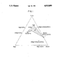
composition 2Al2 O3, 2MgO, 5SiO2 (pure cordierite) and any composition between cordierite and 3Al2 O3, 2SiO2 (mullite) corresponding to the hatched zone in the ternary diagram Al2 O3, MgO, SiO2, FIG. 1.
The operation of shaping the substrate may be carried out in two ways:
the substrate is formed by compression of the powder under a pressure of the order of 150 MPa (between 50 and 400 MPa), and
a process of the "doctor blade" type is used to cast a slip of said powder in an organic or aqueous medium comprising at least 35% by weight of mineral powder, the remainder being composed of solvents, binding agents, plasticising agents and dispersing agents of the type usually employed in that process. After evaporation of the solvents or water, that gives a strip of a thickness of between 50 and 300 μm.
It will be recalled that that method is carried into effect under the following conditions: the slip is introduced into a reservoir, one of the sides of which can be displaced vertically so as to form a calibrated opening through which the suspension flows away. The reservoir is positioned on a strip of polished metal or on a polymer film (for example nylon or polyethylene) or on a glass plate. The reservoir slides over that carrier, wherein the movement can be produced either by displacement of the reservoir or by moving the carrier therepast. Regulation of the opening makes it possible to produce strips, the thickness of which after drying is between 20 and 300 μm.
The copper-based conducting ink which is then deposited on the substrate is primarily formed by pigments in powder form which contain copper, a ceramic powder filler, and an organic phase used as a carrier. The copper-containing pigments which after sintering will give the layers their electrical properties are selected from the following three formulae:
P1 : powder of copper (or copper-based alloy) which is not oxidised
P2 : powder of copper (or copper-based alloy) which is partially oxidised
P3 : powder of oxides of copper in one of the forms Cu2 O, CuO or a mixture of the two.
Among the copper-based alloys, cupro-nickel containing for example from 0.1 to 10% by weight of nickel has the advantage of having a higher melting point than pure copper, which results in a higher degree of convenience in carrying out the co-sintering heat treatment. Those powders containing copper, having a morphology which is as spherical as possible, are of a controlled granulometry such that the mean size of the grains remains between two limits :
from 0.1 to 6 μm for the powders P1 and P2, preferably between 0.2 and 3 μm and
from 0.2 to 10 μm for the powders P3, preferably between 0.5 and 6 μm.
The ceramic powder filler is formed by cordierite having the same characteristics as the powder used for the substrate, the amount introduced being for example between 0.5 and 20% of the mass of copper-based powder and preferably between 1 and 15%.
The amount of pigments based on copper and cordierite powder is between 45 and 80% of the total mass of ink and preferably between 55 and 70%. The organic phase which is composed of solvents, binding agents plasticising agents and dispersing agents of the type usually employed for conducting layers makes it possible to provide the rheological properties necessary for screen printing, it represents from 20 to 55% of the total weight of the ink.
The process for depositing the ink, preferably of screen printing type, is not part of the invention.
After the copper deposit operation, heat treatments have to be applied, which result in the co-sintering effect, the array of parameters defining such treatments depending on the location of the conductors and the nature of the pigment of the ink:
(a) When the product to be produced has only external circuits, the pigment is selected form the three formulae P1 to P3 above and the heat treatment to be carried out is treatment T1 which is defined as follows:
In order to remove the organic components of the ink and the substrate by evaporation and combustion, heating in the air by a slow rise in temperature at a rate which does not exceed 20 K·h-1 with at least one plateau of duration which is at least equal to two hours at a temperature between 200° and 500° C. That step results in at least partial oxidation of the metal copper present in the ink, primarily in the state CuO;
after cooling to ambient temperature, regeneration of the copper by heating in a hydrogen atmosphere, preferably with a temperature rise rate of between 100 and 800 K·h-1, with the temperature being held at the maximum treatment temperature (between 120° C. and 350° C.) for a period of from 10 minutes to 3 hours and with optional intermediate plateaux; it is also possible to operate in an atmosphere of hydrogen diluted with an inert gas;
the arrangement is subjected to a flow of moist argon (or other inert gas) such as moist N2 or He (dew point 20° C.) by bubbling argon into water and the temperature is raised to 1070° C. at a rate of 720 K·h-1
(preferably between 50 and 1000 K·h-1); the addition of water to the inert gas may be replaced by the addition of a small amount of oxygen, which is of the order of a few ppm by volume, for example 5;
a plateau at a temperature of between 1065° and 1080° C. with an optimum in the vicinity of 1070° C. and for a period of between 15 minutes and 2 hours; and
return to ambient temperature in about 3 hours (preferably between 1 hour and 4 hours).
(b) When the product to be produced is a multi-layer substrate comprising both internal and external conductors, the pigment in the ink is selected from the tree formulae P1 to P3, with preferably an ink of formula P2 for the external conductors and heat treatment of type T2 is used, as follows:
heating in the air at between 200° and 500° C.;
after cooling to ambient temperature, regeneration of the copper by heating in hydrogen, preferably with a temperature rise rate of between 100 and 800 K·h-1, with the temperature being held at the maximum treatment temperature for a period of from 10 minutes to 3 hours and with optional intermediate plateaux; it is also possible to operate in an atmosphere of hydrogen diluted with an inert gas;
subjecting the arrangement to a flow of argon (or other inert gas) and a rise in temperature to 950° C. at a rate of 720 K·h-1 (preferably between 500 and 1000 K·h-1);
a plateau at a temperature of 950° C. (preferably between 900° and 1000° C.) for a period of between 15 minutes and 2 hours in the same atmosphere as that used in the temperature rise phase;
subjecting the arrangement to a flow of neutral gas (for example argon) which is moist (dew point 20° C.) at the end of the plateau;
a rise in temperature to 1070° C. in a neutral and moist gas at a rate which is at least equal to 500 K·h-1 ;
a plateau in the same atmosphere at a temperature of between 1065° and 1080° C. with an optimum in the vicinity of 1070° C. and for a period of between 15 minutes and 2 hours; and
return to ambient temperature in about 3 hours (preferably between 1 hour and 4 hours).
All of the above-described solutions are summarised in Table 1; at the same time as a description of the process, they represent examples of use thereof and all result in substrates on which the external conductors are strongly anchored to their carrier while the internal conductors are not bonded to the cordierite, such products being particularly suitable for high-frequency uses as:
the absence of metal-ceramic bond points avoids an increase in the impedance of the internal conductors which do not have compounds of Cu at their surface and which retain a reduced level of surface roughness; and
cordierite has a low dielectric constant (less than 5).
                                  TABLE I                                 
__________________________________________________________________________
                Type of                                                   
                       Principal parameters of the heat treatments        
Products to be produced                                                   
                pigment(ink)                                              
                       Ref.                                               
                          Nature    Atmosphere                            
                                           Temperature °C.         
__________________________________________________________________________
Substrates comprising only                                                
                P1 P2 P3                                                  
                       T1 removal of                                      
                                    air    200 to 500                     
external conductors       organic compounds                               
                          regeneration of Cu                              
                                    H2     120 to 350                     
                          co-sintering                                    
                                    Moist Ar                              
                                           1065 to 1080                   
Multi-layer substrates with                                               
                P1 P2 P3                                                  
                       T2 removal of                                      
                                    Air    200 to 500                     
internal and external conductors                                          
                P3 preferred                                              
                          organic compounds                               
                for external                                              
                          regeneration of Cu                              
                                    H2     120 to 350                     
                conductor co-sintering                                    
                                    Ar      900 to 1000                   
                                    Moist Ar                              
                                           1065 to 1080                   
__________________________________________________________________________

Claims (22)

We claim:
1. A process for co-sintering conductors of copper or copper alloy and a ceramic substrate, comprising the steps of:
(a) shaping a ceramic substrate from a powder consisting essentially of cordierite type ceramic having a sintering temperature lower than 950° C., a specific surface area greater than 50m2 /g, and a chemical composition between 2 Al2 O3 2 MgO 5 SiO2, pure cordierite, and 3 Al2 O3 2 SiO2, mullite;
(b) depositing on an external surface of said substrate a copper-based ink comprising a copper-based powdered pigment and said powder of cordierite type;
(c) heat-treating said substrate with external deposit in a first phase in an oxidizing atmosphere at a temperature not greater than 500° C. to decompose substantially all organic compounds present in the substrate and/or ink;
(d) heat-treating said substrate with external deposit in a second phase in a reducing atmosphere at 120° to 350° C. to regenerate copper; and
(e) heat-treating said substrate with external deposit in a third phase at a temperature plateau at between 1065° and 1080° C. for 15 minutes to 2 hours, at least partially in a flow of moist inert gas for co-sintering, resulting in densification of the cordierite type ceramic of at least 95% with the formation of at least one crystalline phase, and in the formation of a liquid Cu-Cu2 O eutectic from said external deposit which bonds the deposit to the Al2 O3 of the cordierite-type ceramic.
2. A process according to claim 1 wherein the copper is introduced into the ink in the form of a powder based on copper or alloys of copper which is non-oxidised.
3. A process according to claim 1 wherein the copper is introduced into the ink in the form of a powder based on copper or alloy of copper which is partially oxidised.
4. A process according to claim 1 wherein the copper is introduced into the ink in the form of a powder of copper oxide of type Cu2 O, CuO or a mixture of the two.
5. A process according to claim 2 or 3 wherein the mean granulometric size of said copper powder is between 0.1 and 6 μm.
6. A process according to claim 4 wherein the means granulometric size of said powder of copper oxides is between 0.2 and 10 μm.
7. A process according to claim 5 wherein said ink contains cordierite-type powder of the same nature as that used for the substrate and in an amount of between 0.5 and 20% of the weight of copper-based pigments.
8. A process according to claim 7 wherein said ink contains an amount of pigments based on copper and cordierite-type powder which is between 45 and 80% of the total mass of ink.
9. A process according to claim 1 wherein said phase for the decomposition of organic compounds is carried out in air by a slow rise in temperature at a rate which does not exceed 20 K·h-1 with at least one plateau of a duration which is at least equal to two hours at a temperature between 200° and 500° C.
10. A process according to claim 1 wherein said phase for the regeneration of copper is effected in an atmosphere of hydrogen in pure form or diluted with inert gas at a temperature of between 120° and 350° C., with a rise in temperature of between 100 and 800 K·h-1 and with the temperature being held at the treatment temperature for a period of from 10 minutes to 3 hours.
11. A process according to claim 1 wherein said phase of co-sintering is effected with a rise in temperature of between 500 and 100 K·h-1.
12. A process according to claim 11 wherein said phase of co-sintering is carried out in a flow of moist argon.
13. A process according to claim 11 wherein said flow of moist inert gas is introduced as from the end of said phase for regeneration of the copper in a reducing atmosphere.
14. A process according to claim 13 for the production of substrates of ceramic comprising only external conductors.
15. A process according to claim 5, wherein the mean granulometric size of said copper powder is between 0.2 and 3 μm.
16. A process according to claim 6, wherein the mean granulometric size of said powder of copper oxides is between 0.5 and 6 μm.
17. A process according to claim 7, wherein the amount of said cordierite-type powder is between 1 and 15% of the weight of copper based pigments.
18. A process according to claim 8, wherein the amount of said pigments and cordierite-type powder is between 55 and 70% of the total mass of the ink.
19. A process according to claim 11, wherein the temperature of said substrate is raised after said second phase to 950° C. in an inert gas, and a flow of said moist inert gas is begun after the temperature has reached 950° C.
20. A process according to claim 17 or 18, wherein said moist inert gas has a dew point of 20° C.
21. A process according to claim 19 for the production of multi-layer substrates of ceramic material comprising internal and external conductors.
22. A process for co-sintering conductors of copper or copper alloy and a ceramic substrate, comprising the steps of:
(a) shaping a plurality ceramic substrates from a powder consisting essentially of cordierite type ceramic having a sintering temperature lower than 950° C., a specific surface area greater than 50m2 /g, and a chemical composition between 2 Al2 O3 2 MgO 5 SiO2, pure cordierite, and 3 Al2 O3 2 SiO2, mullite;
(b) depositing on each said substrate a copper-based ink comprising a copper-based powdered pigment and said powder or cordierite type;
(c) forming from said substrate a multi-layer structure comprising internal and external conductors.
(d) heat-treating said multi-layer structure in a first phase in an oxidizing atmosphere at a temperature not greater than 500° C. to decompose substantially all organic compounds present in the substrate and/or ink;
(e) heat-treating said multi-layer structure in a second phase in a reducing atmosphere at 120° to 350° C. to regenerate copper;
(f) heat-treating said multi-layer structure in a third phase in an inert gas at a temperature plateau of 900°-1000° C. for 15 minutes to 2 hours; and
(g) heat-treating said multi-layer structure in a fourth phase at a temperature plateau of between 1065° and 1080° C. for 15 minutes to 2 hours, at least partially in a flow of moist inert gas, resulting in densification of the cordierite-type ceramic of at least 95% with the formation of liquid Cu-Cu2 O eutectic from said at least one external conductor which bonds said external conductor to the Al2 O3 of the cordierite-type ceramic, said at least one internal conductor remaining substantially unbonded to a substrate surface.
US07/299,335 1988-01-22 1989-01-23 Process for co-sintering conductors of copper or copper-base alloys and their ceramic substrate of cordierite Expired - Fee Related US4915899A (en)

Applications Claiming Priority (2)

Application Number Priority Date Filing Date Title
FR8801136 1988-01-22
FR8801136A FR2626270B1 (en) 1988-01-22 1988-01-22 PROCESS FOR COFRITTING, COPPER CONDUCTORS OR COPPER-BASED ALLOYS AND THEIR CERAMIC SUBSTRATE IN CORDIERITY

Publications (1)

Publication Number Publication Date
US4915899A true US4915899A (en) 1990-04-10

Family

ID=9362822

Family Applications (1)

Application Number Title Priority Date Filing Date
US07/299,335 Expired - Fee Related US4915899A (en) 1988-01-22 1989-01-23 Process for co-sintering conductors of copper or copper-base alloys and their ceramic substrate of cordierite

Country Status (4)

Country Link
US (1) US4915899A (en)
EP (1) EP0326499A1 (en)
JP (1) JPH0632363B2 (en)
FR (1) FR2626270B1 (en)

Cited By (4)

* Cited by examiner, † Cited by third party
Publication number Priority date Publication date Assignee Title
US5230846A (en) * 1990-10-11 1993-07-27 The Boc Group, Inc. Method for preparing multilayered ceramic with internal copper conductor
AU644481B2 (en) * 1990-10-11 1993-12-09 Boc Group, Inc., The Method for preparing multi-layered ceramic with internal copper conductor
US5302181A (en) * 1991-04-26 1994-04-12 Kubota Corporation Oxide-dispersion-strengthened heat-resistant chromium-based sintered alloy
EP3173392B1 (en) * 2015-11-27 2021-04-21 maxon international ag Method for producing ceramic parts

Families Citing this family (3)

* Cited by examiner, † Cited by third party
Publication number Priority date Publication date Assignee Title
DE4100145A1 (en) * 1990-01-10 1991-07-11 Murata Manufacturing Co Integrated circuit assembly substrate - has metal-ceramic composite material, with metal filling holes in ceramic plate
US5682018A (en) * 1991-10-18 1997-10-28 International Business Machines Corporation Interface regions between metal and ceramic in a metal/ceramic substrate
CN101628195B (en) * 2009-07-22 2014-01-15 河北理工大学 High-temperature gas filter supporting body and preparation method thereof

Citations (2)

* Cited by examiner, † Cited by third party
Publication number Priority date Publication date Assignee Title
US3994430A (en) * 1975-07-30 1976-11-30 General Electric Company Direct bonding of metals to ceramics and metals
US4551357A (en) * 1984-05-25 1985-11-05 Ngk Insulators, Ltd. Process of manufacturing ceramic circuit board

Family Cites Families (6)

* Cited by examiner, † Cited by third party
Publication number Priority date Publication date Assignee Title
JPS5826680B2 (en) * 1975-10-07 1983-06-04 富士通株式会社 Ceramic warm air conditioner
US4340436A (en) * 1980-07-14 1982-07-20 International Business Machines Corporation Process for flattening glass-ceramic substrates
JPS61292392A (en) * 1985-06-20 1986-12-23 松下電器産業株式会社 Manufacture of ceramic wiring board
FR2585181B1 (en) * 1985-07-16 1988-11-18 Interconnexions Ceramiques METHOD FOR MANUFACTURING AN INTERCONNECTION SUBSTRATE FOR ELECTRONIC COMPONENTS, AND SUBSTRATE OBTAINED BY ITS IMPLEMENTATION
FR2585015A1 (en) * 1985-07-16 1987-01-23 Centre Nat Rech Scient CERAMIC POWDER OF FRITTABLE CORDIERITY TYPE AT LOW TEMPERATURE, PROCESS FOR PREPARATION AND CERAMIC COMPOSITION OBTAINED BY FRITTING THE POWDER
JPS62113758A (en) * 1985-10-25 1987-05-25 株式会社住友金属セラミックス Low temperature burnt ceramics

Patent Citations (2)

* Cited by examiner, † Cited by third party
Publication number Priority date Publication date Assignee Title
US3994430A (en) * 1975-07-30 1976-11-30 General Electric Company Direct bonding of metals to ceramics and metals
US4551357A (en) * 1984-05-25 1985-11-05 Ngk Insulators, Ltd. Process of manufacturing ceramic circuit board

Cited By (4)

* Cited by examiner, † Cited by third party
Publication number Priority date Publication date Assignee Title
US5230846A (en) * 1990-10-11 1993-07-27 The Boc Group, Inc. Method for preparing multilayered ceramic with internal copper conductor
AU644481B2 (en) * 1990-10-11 1993-12-09 Boc Group, Inc., The Method for preparing multi-layered ceramic with internal copper conductor
US5302181A (en) * 1991-04-26 1994-04-12 Kubota Corporation Oxide-dispersion-strengthened heat-resistant chromium-based sintered alloy
EP3173392B1 (en) * 2015-11-27 2021-04-21 maxon international ag Method for producing ceramic parts

Also Published As

Publication number Publication date
JPH0632363B2 (en) 1994-04-27
FR2626270A1 (en) 1989-07-28
FR2626270B1 (en) 1992-04-30
EP0326499A1 (en) 1989-08-02
JPH01238191A (en) 1989-09-22

Similar Documents

Publication Publication Date Title
EP0164028B1 (en) Mullite-cordierite composite ceramic
US5468445A (en) Ceramic via composition, multilayer ceramic circuit containing same, and process for using same
US5215610A (en) Method for fabricating superconductor packages
US5145540A (en) Ceramic composition of matter and its use
US6110596A (en) Silicon nitride ceramic circuit substrate and semiconductor device using the same
EP0196670B1 (en) Ceramic substrates for microelectronic circuits and process for producing same
JPWO2002045470A1 (en) Substrate and method of manufacturing the same
US4915899A (en) Process for co-sintering conductors of copper or copper-base alloys and their ceramic substrate of cordierite
JP3408298B2 (en) High thermal conductive silicon nitride metallized substrate, method of manufacturing the same, and silicon nitride module
KR20020062308A (en) Joint body of glass-ceramic and aluminum nitride sintered compact and method for producing the same
JP2000188453A (en) Wiring substrate and its manufacture
WO1989001461A1 (en) Co-sinterable metal-ceramic packages and materials therefor
US5702807A (en) Ceramic circuit board and manufacturing method thereof
JPH0544840B2 (en)
JPS6153156A (en) Mulite beta-spodumene composite ceramic
JPS62216983A (en) Aluminum nitride sintered body with metallization layer and manufacture
JP3125500B2 (en) Ceramic substrate
JPS60245154A (en) Multilayer substrate for mounting semiconductor device
JP3898400B2 (en) Wiring board and manufacturing method thereof
JP3336176B2 (en) Glass ceramic sintered body
JP3314131B2 (en) Wiring board
JPH0337758B2 (en)
JPS61230396A (en) Manufacture of high heat conductivity multilayer ceramic wiring substrate
JPH09237957A (en) Alumina circuit board and manufacture thereof
JPS61230399A (en) Manufacture of high heat conductivity multilayer ceramic wiring substrate

Legal Events

Date Code Title Description
AS Assignment

Owner name: PECHINEY RECHERCHE GROUPEMENT D'INTERET ECONOMIQUE

Free format text: ASSIGNMENT OF ASSIGNORS INTEREST.;ASSIGNORS:OLIVER, VERONIQUE;GUILLE, JEAN-LOUIS;BERNIER, JEAN-CLAUDE;AND OTHERS;REEL/FRAME:005027/0220;SIGNING DATES FROM 19890203 TO 19890208

CC Certificate of correction
FEPP Fee payment procedure

Free format text: PAYOR NUMBER ASSIGNED (ORIGINAL EVENT CODE: ASPN); ENTITY STATUS OF PATENT OWNER: LARGE ENTITY

FPAY Fee payment

Year of fee payment: 4

REMI Maintenance fee reminder mailed
LAPS Lapse for failure to pay maintenance fees
FP Lapsed due to failure to pay maintenance fee

Effective date: 19980415

STCH Information on status: patent discontinuation

Free format text: PATENT EXPIRED DUE TO NONPAYMENT OF MAINTENANCE FEES UNDER 37 CFR 1.362